 | –≠–ª–µ–∫—Ç—Ä–æ–Ω–Ω—ã–π –∫–æ–º–ø–æ–Ω–µ–Ω—Ç: TC6320TG | –°–∫–∞—á–∞—Ç—å:  PDF PDF  ZIP ZIP |
TC6320
________________________________________________________________________________
Supertex Inc. does not recommend the use of its products in life support applications and will not knowingly sell its products for use in such applications unless it receives an adequate
"products liability indemnification insurance agreement." Supertex does not assume responsibility for use of devices described and limits its liability to the replacement of devices
determined to be defective due to workmanship. No responsibility is assumed for possible omissions or inaccuracies. Circuitry and specifications are subject to change without notice. For
the latest product specifications, refer to the Supertex website: http://www.supertex.com. For complete liability information on all Supertex products, refer to the most current databook or
to the Legal/Disclaimer page on the Supertex website.
Initial Release
N- and P-Channel Enhancement-Mode MOSFET Pair
Features
Integrated gate-source resistor
Integrated gate-source zener diode
Low threshold
Low on-resistance
Independent N- and P-channels
Electrically isolated N- and P-channels
Low input capacitance
Fast switching speeds
Free from secondary breakdowns
Low input and output leakage
Application
High voltage pulsers
Amplifiers
Buffers
Piezoelectric transducer drivers
General purpose line drivers
Logic level interfaces
Absolute Maximum Ratings*
Drain-to-Source Voltage
BV
DSS
Drain-to-Gate Voltage
BV
DGS
Operating and Storage Temperature
-55∞C to +150∞C
Soldering Temperature*
300∞C
*Distance of 1.6mm from case for 10 seconds.
General Description
The Supertex TC6320TG consists of a high voltage low
threshold N-channel and P-channel MOSFET in an SO-8
package. Both MOSFETs have integrated gate-source
resistors and gate-source zener diode clamps which are
desired for high voltage pulser applications. TC6320TG, a
complementary high-speed, high voltage, gate-clamped
N- and P-channel MOSFET pair in a single SO-8
package. The TC6320TG offers 200V breakdown voltage,
2.0A output peak current and low input capacitance. The
2.0A output current capability will minimize rise and fall
times. The low input capacitance will minimize
propagation delay times and also rise and fall times. The
MOSFETs have integrated gate-source resistors and
gate-source zener diode clamps that are desired for high
voltage pulser applications saving board space and
improving performance. It is specifically designed for
applications in medical ultrasound transmitters and non-
destructive evaluation in materials flaw detection, but it
can also be used as an efficient buffer.
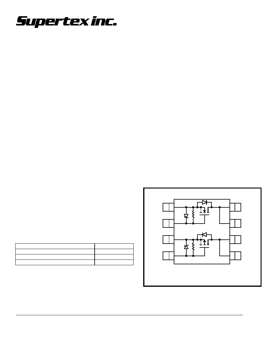
Package Option
S1
G1
S2
G2
D2
D2
D1
D1
SO-8 Package
(top view)
N-Channel
P-Channel
1
2
3
4
5
6
7
8

TC6320
________________________________________________________________________________
Supertex, Inc. January 21, 2003
2
BV
DSS
/ BV
DGS
R
DS(ON)
(max)
Order Number / Package
N-Channel P-Channel N-Channel P-Channel
SO-8
200V -200V 7.0
8.0
TC6320TG
N-Channel Electrical Characteristics
(at T
A
=25∞C unless otherwise specified)
Symbol Parameter
Min Typ Max Units Conditions
BV
DSS
Drain-to-Source
Breakdown Voltage
200 V V
GS
=0V, I
D
=2mA
V
GS(th)
Gate Threshold Voltage
1.0
2.0
V
V
GS
=V
DS
, I
D
=1mA
V
GS(th)
Change in V
GS(th)
with Temperature
-4.5
mV/∞C V
GS
=V
DS
, I
D
=1mA
R
GS
Gate-Source Shunt Resistor
10
50
K
I
GS
=100µA
R
GS
Change in R
GS
with Temperature
TBD
%/∞C
I
GS
=100µA
Vz
GS
Gate-Source Zener Voltage
13.2
25
V
I
GS
=2mA
Vz
GS
Change in Vz
GS
with Temperature
TBD
mV/∞C I
GS
=2mA
10
µA
V
GS
=0V, V
DS
=Max Rating
I
DSS
Zero Gate Voltage Drain Current
1.0
mA
V
GS
=0V, V
DS
=0.8 Max
Rating, T
A
=125∞C
1.0
V
GS
=4.5V, V
DS
=25V
I
D(ON)
On-State Drain Current
2.0
A
V
GS
=10V, V
DS
=25V
8.0
V
GS
=4.5V, I
D
=150mA
R
DS(ON)
Static
Drain-to-Source
ON-State Resistance
7.0
V
GS
=10V, I
D
=1.0A
R
DS(ON)
Change in R
DS(ON)
with Temperature
1.0
%/∞C
V
GS
=4.5V, I
D
=150mA
G
FS
Forward
Transconductance
400
mmho
V
DS
=25V, I
D
=200mA
C
ISS
Input
Capacitance
110
C
OSS
Common Source Output Capacitance
60
C
RSS
Reverse Transfer Capacitance
23
pF
V
GS
=0V, V
DS
=25V
f=1MHz
t
d(ON)
Turn-ON Delay Time
10
t
r
Rise
Time
15
t
d(OFF)
Turn-Off Delay Time
20
t
f
Fall
Time
15
ns
V
DD
=25V,
I
D
=1.0A
R
GEN
=25
V
SD
Diode Forward Voltage Drop
1.8
V
V
GS
=0V, I
SD
=0.5A
t
rr
Reverse Recovery Time
300
ns
V
GS
=0V, I
SD
=0.5A
Notes:
1) All DC parameters 100% tested at 25∞C unless otherwise stated. (Pulsed test: 300µs pulse at 2% duty cycle.)
2) All AC parameters sample tested.
N-Channel Switching Waveforms and Test Circuit
R
GEN
Input
Pulse
Generator
V
DD
R
L
D.U.T
OUTPUT
10V
0V
0V
V
DD
t
d(OFF)
Input
Output
t
r
t
f
t
d(ON)
t
(ON)
t
(OFF)
10%
90%
90%
10%
90%
10%

TC6320
________________________________________________________________________________
P-Channel Electrical Characteristics
(at T
A
=25∞C unless otherwise specified)
Symbol Parameter
Min Typ Max Units Conditions
BV
DSS
Drain-to-Source
Breakdown Voltage
-200 V V
GS
=0V, I
D
=-2mA
V
GS(th)
Gate Threshold Voltage
-1.0
-2.4
V
V
GS
=V
DS
, I
D
=-1mA
V
GS(th)
Change in V
GS(th)
with Temperature
4.5
mV/∞C V
GS
=V
DS
, I
D
=-1mA
R
GS
Gate-Source Shunt Resistor
10
50
K
I
GS
=-100µA
R
GS
Change in R
GS
with Temperature
TBD
%/∞C
I
GS
=-100µA
Vz
GS
Gate-Source Zener Voltage
13.2
25
V
I
GS
=-2mA
V
GS(th)
Change in Vz
GS
with Temperature
TBD
mV/∞C I
GS
=-2mA
-10
µA
V
GS
=0V, V
DS
=Max Rating
I
DSS
Zero Gate Voltage Drain Current
-1.0
mA
V
GS
=0V, V
DS
=0.8 Max
Rating, T
A
=125∞C
-1.0
V
GS
=-4.5V, V
DS
=-25V
I
D(ON)
On-State Drain Current
-2.0
A
V
GS
=-10V, V
DS
=-25V
10
V
GS
=-4.5V, I
D
=-150mA
R
DS(ON)
Static
Drain-to-Source
ON-State Resistance
8.0
V
GS
=-10V, I
D
=-1.0A
R
DS(ON)
Change in R
DS(ON)
with Temperature
1.0
%/∞C
V
GS
=-10V, I
D
=-200mA
G
FS
Forward
Transconductance
400
mmho
V
DS
=-25V, I
D
=-200mA
C
ISS
Input
Capacitance
200
C
OSS
Common Source Output Capacitance
55
C
RSS
Reverse Transfer Capacitance
30
pF
V
GS
=0V, V
DS
=-25V
f=1MHz
t
d(ON)
Turn-ON Delay Time
10
t
r
Rise
Time
15
t
d(OFF)
Turn-Off Delay Time
20
t
f
Fall
Time
15
ns
V
DD
=-25V,
I
D
=-1.0A
R
GEN
=25
V
SD
Diode Forward Voltage Drop
-1.8
V
V
GS
=0V, I
SD
=-0.5A
t
rr
Reverse Recovery Time
300
ns
V
GS
=0V, I
SD
=-0.5A
Notes:
1) All DC parameters 100% tested at 25∞C unless otherwise stated. (Pulsed test: 300µs pulse at 2% duty cycle.)
2) All AC parameters sample tested.
P-Channel Switching Waveforms and Test Circuit
R
GEN
Input
Pulse
Generator
V
DD
R
L
D.U.T
OUTPUT
0V
-10V
0V
V
DD
t
d(OFF)
Input
Output
t
r
t
f
t
d(ON)
t
(ON)
t
(OFF)
90%
10%
90%
10%
10%
90%
1/22/03