1
General Description
The Supertex HV9100 through HV9103 are a series of BiCMOS/
DMOS single-output, pulse width modulator ICs intended for use
in high-speed high-efficiency switchmode power supplies. They
provide all the functions necessary to implement a single-switch
current-mode PWM, in any topology, with a minimum of external
parts.
Utilization of Supertex proprietary BiCMOS/DMOS technology
results in a device with one tenth of the operating power of
conventional bipolar PWM ICs, which can operate at more than
twice their switching frequency. Dynamic range for regulation is
also increased, to approximately 8 times that of similar bipolar
parts. They start directly from any DC input voltage between 10
and 70VDC for the HV9100 or 10 to 120VDC for the HV9102 and
HV9103, requiring no external power resistor. The output stage
for the HV9100 is a 150V, 5.0 ohm MOSFET and for the HV9102
and HV9103 is a 200V, 7.0 ohm MOSFET. The clock frequency
is set with a single external resistor.
Accessory functions are included to permit fast remote shutdown
(latching or nonlatching), and undervoltage shutdown.
Absolute Maximum Ratings
+V
IN
, Input Voltage
120V
V
DS
200V
V
DD
, Logic Voltage
15.0V
Input Voltage Logic, Linear, FB and Sense -0.3V to V
DD
+0.3V
I
D
(Peak)
2.5A
Storage Temperature
-65
∞C to 150∞C
Power Dissipation, Plastic DIP
750mW
Power Dissipation, PLCC
1400mW
Applications
DC/DC Converters
Distributed Power Systems
ISDN Equipment
PBX Systems
Modems
Features
10 to 120V input range
200V, 7.0 output MOSFET
Current-Mode Control
High Efficiency
Up to 1MHz Internal Oscillator
Internal Start-up Circuit
+V
IN
Feedback
Max MOSFET Switch
Package Options
Min
Max
Voltage
Duty Cycle
BV
DSS
R
DS (ON)
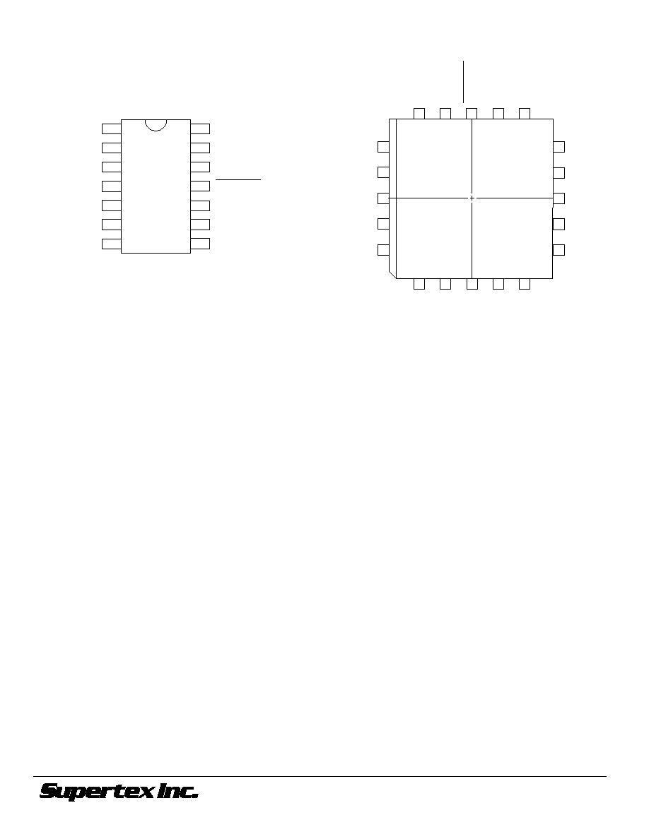
14 Pin Plastic DIP
20 Pin Plastic PLCC
10V
70V
± 1.0%
49%
150V
5.0
HV9100P
HV9100PJ
10V
120V
± 1.0%
49%
200V
7.0
HV9102P
HV9102PJ
10V
120V
±1.0%
99%
200V
7.0
HV9103P
HV9103PJ
Standard temperature range for all parts is industrial (-40
∞ to +85∞C).
Ordering Information
High-Voltage Switchmode Controllers with MOSFET
For detailed circuit and application information, please refer
to application notes AN-H13 and AN-H21 to AN-H24.
HV9100
HV9102
HV9103
11/12/01
Supertex Inc. does not recommend the use of its products in life support applications and will not knowingly sell its products for use in such applications unless it receives an adequate "products liability
indemnification insurance agreement." Supertex does not assume responsibility for use of devices described and limits its liability to the replacement of devices determined to be defective due to
workmanship. No responsibility is assumed for possible omissions or inaccuracies. Circuitry and specifications are subject to change without notice. For the latest product specifications, refer to the
Supertex website: http://www.supertex.com. For complete liability information on all Supertex products, refer to the most current databook or to the Legal/Disclaimer page on the Supertex website.

6
HV9100/HV9102/HV9103
Reference
The reference consists of a stable bandgap reference followed by
a buffer amplifier which scales the voltage up to approximately
4.0V. The scaling resistors of the reference buffer amplifier are
trimmed during manufacture so that the output of the error
amplifier when connected in a gain of -1 configuration is as close
to 4.000V as possible. This nulls out any input offset of the error
amplifier. As a consequence, even though the observed refer-
ence voltage of a specific part may not be exactly 4V, the feedback
voltage required for proper regulation will be 4V.
A resistor of approximately 50K
is placed internally between the
output of the reference buffer amplifier and the circuitry it feeds
(reference output pin and NON-INVERTING input to the error
amplifier). This allows overriding the internal reference with a low-
impedance voltage source
6V. Using an external reference
reinstates the input offset voltage of the error amplifier, and its
effect of the exact value of feedback voltage required. In general,
because the reference voltage of the Supertex HV910x is not
noisy, as some previous devices have been, overriding the
reference should seldom be necessary.
Because the reference is a high impedance node, and usually
there will be significant electrical noise near it, a bypass capacitor
between the reference pin and V
SS
is strongly recommended. The
reference buffer amplifier is intentionally compensated to be
stable with a capacitive load of 0.01 to 0.1
µF.
Error Amplifier
The error amplifier is a true low-power differential input opera-
tional amplifier intended for around-the-amplifier compensation.
It is of mixed CMOS-bipolar construction: a PMOS input stage is
used so the common-mode range includes ground and the input
impedance is very high. This is followed by bipolar gain stages
which provide high gain without the electrical noise of all-MOS
amplifiers. The amplifier is unity-gain stable.
Current Sense Comparators
The HV910x uses a true dual comparator system with indepen-
dent comparators for modulation and current limiting. This allows
the designer greater latitude in compensation design, as there are
no clamps (except ESD protection) on the compensation pin. Like
the error amplifier, the comparators are of low-noise BiCMOS
construction.
Remote Shutdown
The shutdown and reset pins can be used to perform either
latching or non-latching shutdown of a converter as required.
These pins have internal current source pull-ups so they can be
driven from open-drain logic. When not used, they should be left
open, or connected to V
DD
.
Main Switch
The main switch is a normal N-channel power MOSFET. Unlike
the situation with competitive devices, the body diode can be used
if desired without destroying the chip.
Preregulator
The preregulator/startup circuit for the HV910x consists of a high-
voltage N-channel depletion-mode DMOS transistor driven by an
error amplifier to form a controlled current path between the V
IN
terminal and the V
DD
terminal. Maximum current (about 20 mA)
occurs when V
DD
= 0, with current reducing as V
DD
rises. This path
shuts off altogether when V
DD
rises to somewhere between 7.8
and 9.4V, so that if V
DD
is held at 10 or 12V by an external source
(generally the supply the chip is controlling) no current other than
leakage is drawn through the high voltage transistor. This mini-
mizes dissipation.
An external capacitor between V
DD
and V
SS
is generally required
to store energy used by the chip during the time between shutoff
of the high voltage path and the V
DD
supply's output rising enough
to take over the powering of the chip. This capacitor generally also
serves as the output filter capacitor for that output from the supply.
1
µF is generally sufficient to assure against double-starting.
Capacitors as small as 0.1
µF can work when faster response from
the V
DD
line is required. Whatever capacitor is chosen should
have very good high frequency characteristics. Stacked polyester
or ceramic capacitors work well. Electrolytic capacitors are gen-
erally not suitable.
A common resistor divider string is used to monitor V
DD
for both
the undervoltage lockout circuit and the shutoff circuit of the high
voltage FET. Setting the undervoltage sense point about 0.6V
lower on the string than the FET shutoff point guarantees that the
undervoltage lockout always releases before the FET shuts off.
Bias Circuit
An external bias resistor, connected between the bias pin and V
SS
is required to set currents in a series of current mirrors used by the
analog sections of the chip. Nominal external bias current require-
ment is 15 to 20
µA, which can be set by a 390K to 510K
resistor if a 10V V
DD
is used, or a 510K
to 680K resistor if a 12V
V
DD
is used. A precision resistor is NOT required;
± 5% is fine.
For extremely low power operation, the value of bias current can
be reduced to as low as 5
µA by further increases in the value of
the bias resistor. This will reduce quiescent current by about a
third, reduce bandwidth of the error amp by about half, and slow
the current sense comparator by about 30%.
Clock Oscillator
The clock oscillator of the HV910x consists of a ring of CMOS
inverters, timing capacitors, a capacitor discharge FET, and, in
the 50% maximum duty cycle versions, a frequency dividing flip-
flop. A single external resistor between the OSC In and OSC Out
pins is required to set oscillator frequency (see Fig. 4). For the
50% maximum duty cycle versions the `Discharge' pin is internally
connected to GND. For the 99% duty cycle version, `Discharge'
can either be connected to V
SS
directly or connected to V
SS
through a resistor used to set a deadtime.
One difference exists between the Supertex HV910x and com-
petitive parts. The oscillator of the HV910x is shut off when a
shutoff command is received. This saves about 150
µA of quies-
cent current, which aids in situations where an absolute minimum
of quiescent power dissipation is required.
Technical Description