 | –≠–ª–µ–∫—Ç—Ä–æ–Ω–Ω—ã–π –∫–æ–º–ø–æ–Ω–µ–Ω—Ç: EYSF2CAXX | –°–∫–∞—á–∞—Ç—å:  PDF PDF  ZIP ZIP |


PRELIMINARY
∑The module is a Max.4dBm( Class2 ) module.
∑Bluetooth
Æ
standard Ver1.1 conformity.
∑Internal baseband clock oscillator.
∑Internal 1.8V regulator
∑Low current consumption
∑Support functions
Serial Port Emulation (Point-To-Point)
∑ Interface: UART
∑ Protocol Stack/Profile (L2CAP,RFCOMM,SDP,GAP,SPP)
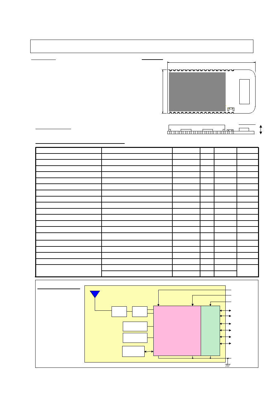
∑Small outline.
15.4
x
10
x
2.0
mm
Bluetooth
Æ
Module
Simple Cable Replacement
TAIYO YUDEN
Features
Outline
∑ POS,Barcode Reader,FA equipments
Applications
Jun./2003 Ver.1.1
EYSF2CA**-**
General Electrical Specification
mA
-
TBD
Receive DM1 Packet
Average Current Consumption
V
3.60
3.30
3.00
Operating Voltage (VDD_PIO)
V
VDD_PIO+0.30
-
0.70VDD_PIO
RESET, UART, GPIO
Input High Voltage
V
0.40
-
-
UART, GPIO
Output Low Voltage
V
-
-
VDD_PIO-0.40
UART, GPIO
Output High Voltage
V
0.80
-
-0.30
RESET, UART, GPIO
Input Low Voltage
-
5:1
No abnormal Oscillation
Load Impedance
dBm
-70
-83
RX Sensitivity
dBm
4
0
-6
measured in 50 ohm
RF Output Power
V
3.60
3.30
3.00
Operating Voltage (VDD_MEM)
GHz
2.480
2.402
Carrier Frequency
Units
Max.
Typ.
Min.
Description
Parameter
Block Diagram
2.2
1x11
2.2
10
15.4
2.
0
Unit: mm
RFCOMM
L2CAP
SDP
LMP
LED, Baudrate, Role, Op Mode
UART
Balun
I/O
Flash
Memory
Xtal
Loop Filter
RF + BB
B.P.F
VDD_PIO
UART(4)
SPI(4)
LED(2)
Operation Mode
VDD_MEM
GND(6)
Baud Rate(3)
Role
RESET
Regulator
RF_IN-OUT
Note:The above PRELIMINARY data are not guaranteed,and are subject to change without notice.
The Bluetooth
Æ
word mark and logos are owned by the Bluetooth SIG, Inc. and any use of such marks
by TAIYO YUDEN CO.,LTD. is under license.

Balun
I/O
Flash
Memory
RF_IN-OUT
Xtal
Loop Filter
Regulator
RF + BB
B.P.F
SIDBAND(3)
VDD_PIO
USB(2)
UART(4)
PCM(4)
SPI(4)
GPIO(5)
RESET
VDD _MEM
GND(6)
PRELIMINARY
∑The module is a Max.4dBm( Class2 ) module.
∑Bluetooth
Æ
standard Ver. 1.2 conformity.
∑Internal baseband clock oscillator.
∑Internal 1.8V regulator
∑Low current consumption
∑Support functions
SCO links,ACL links,Piconet<7>,Hold,Sniff,Park, AFH, Faster connection
∑Interface:EYSF2CSXX: USB(for data and voice)
∑Protocol stack:Under HCI firmware
∑Small outline.
15.4
x
10
x
2.0
mm
Bluetooth
Æ
Module
Class2 USB Full Module
TAIYO YUDEN
Features
Outline
∑Notebook PC
∑PDA
Applications
Nov./2003 Ver.2.0
EYSF2CSXX
General Electrical Specification
V
0.30
-
-
D+, D-
Output Low Voltage
V
3.45
3.30
3.10
Operating Voltage (VDD_PIO)
V
VDD_PIO+0.30
-
0.70VDD_PIO
RESET, SIDBAND, GPIO
Input High Voltage
V
0.80
-
D+, D-
Input Low Voltage
V
0.40
-
-
SIDBAND, GPIO
Output Low Voltage
V
-
-
2.00
D+, D-
Input High Voltage
V
-
-
2.80
D+, D-
Output High Voltage
V
-
-
VDD_PIO-0.40
SIDBAND, GPIO
Output High Voltage
mA
-
48
Receive DM1
Average Current Consumption
V
0.80
-
-0.30
RESET, SIDBAND, GPIO
Input Low Voltage
-
5:1
No abnormal Oscillation
Load Impedance
dBm
-70
-83
RX Sensitivity
dBm
4
0
-6
measured in 50 ohm
RF Output Power
V
3.45
3.30
3.10
Operating Voltage (VDD_MEM)
GHz
2.480
2.402
Carrier Frequency
Units
Max.
Typ.
Min.
Description
Parameter
Block Diagram
2.2
1x11
2.2
10
15.4
2.
0
Unit: mm
Note: The above PRELIMINARY data are not guaranteed and are subject to change without notice.
The Bluetooth
Æ
word mark and logos are owned by the Bluetooth SIG, Inc. and any use of such marks by TAIYO YUDEN CO., LTD. is under license.
Balun
I/O
Flash
Memory
VDD_PIO
USB(2)
SPI(4)
PIO(12)
AIO(2)
RESET
VDD_MEM
VDD_1.8V
GND(6)
Antenna
Xtal
Loop Filter
RF + BB
B.P.F
UART(4)
PRELIMINARY
Nov./2003 Ver.2.0
∑ Antenna is provided on board
∑The module is Max.4 dBm( Class2 )module
∑ Bluetooth
Æ
standard Ver. 1.2 conformity
∑ Internal baseband clock oscillator
∑ Low current consumption
∑ Support functions
ACL links, Piconet<7>, Hold, Sniff, Park
, AFH, Faster connection
∑ Interface: UART
∑ HCI module
∑ Outline:
34.0
x
15.6
x
3.7
mm
Class 2 UART All In One(ANT+RF+BB)
TAIYO YUDEN
∑ PC & peripheral
EYMF2CAMM
Features
Outline
Applications
General Electrical Specification
Bluetooth
Æ
Module
mA
-
14
Receive DM1
(VDD_MEM,VDD_PIO)
Average Current Consumption
Degree C
70
25
0
Operation temperature range
V
3.6
3.3
3.0
VDD_MEM = VDD_PIO
Operating Voltage(VDD_PIO)
V
1.9
1.8
1.75
Operating Voltage(VDD_1.8)
V
VDD +0.3
0.7VDD_PIO
RESET
Input High Voltage
V
0.8
-0.3
RESET
Input Low Voltage
V
-
VDD -0.4
PIO, AIO, SPI
Output High Voltage
V
0.4
-
UART_TX, UART_RTS
Output Low Voltage
-
35
Receive DM1
(VDD_1.8)
V
-
VDD -0.4
UART_TX, UART_RTS
Output High Voltage
V
0.4
-
PIO, AIO, SPI
Output Low Voltage
V
VDD +0.3
0.7VDD_PIO
UART_RX, UART_CTS
Input High Voltage
V
VDD +0.3
0.7VDD_PIO
PIO, AIO, SPI
Input High Voltage
V
0.8
-0.3
UART_RX, UART_CTS
Input Low Voltage
V
0.8
-0.3
PIO, AIO, SPI
Input Low Voltage
-
5:1
-
No abnormal Oscillation
Load Impedance
dBm
-70
-83
-
RX Sensitivity
dBm
4
0
-6
Measured in 50 ohm
RF Output Power
V
3.6
3.3
3.0
VDD_MEM = VDD_PIO
Operating Voltage(VDD_MEM)
GHz
2.480
2.402
Carrier Frequency
Units
Max.
Typ.
Min.
Description
Parameter
34
15.6
3.7
Unit: mm
Note: The above PRELIMINARY data are not guaranteed and are subject to change without notice.
The Bluetooth
Æ
word mark and logos are owned by the Bluetooth SIG, Inc. and any use of such marks by TAIYO YUDEN CO., LTD. is under license.
Block Diagram