 | –≠–ª–µ–∫—Ç—Ä–æ–Ω–Ω—ã–π –∫–æ–º–ø–æ–Ω–µ–Ω—Ç: 5002CL | –°–∫–∞—á–∞—Ç—å:  PDF PDF  ZIP ZIP |
TDK SEMICONDUCTOR CORP.
Æ
AVPro
Æ
5002CL
Dual SCART A/V Switch
PRELIMINARY
DATASHEET
January 2003
DESCRIPTION
The AVPro
Æ
5002CL device is an audio/video switching
IC that supports an input/output port, an input only port,
and an output only port. The device includes
multiplexers that allow the inputs to be routed to the
outputs in various configurations. Additional outputs are
provided to drive an external RF modulator. The video
outputs of the multiplexers are buffered to drive 137
loads. The audio outputs are buffered to provide 2
Vrms output into a 600 load. The 5002CL has
features optimized for Canal+ satellite receiver
applications, but it can also be used in other
applications that require control of multiple audio and
video sources.
FEATURES
∑ Two SCART connections (Auxiliary, TV)
∑ Video section
- Integrated output drivers
- RGB, SVHS, composite outputs
- Programmable RGB gain
∑ Audio section
- Dual mode volume control
0 or 6 dB gain, plus 0 to -31 dB attenuation (1 dB
step)
- Programmable gain on DAC input channels
- Ground based outputs (no AC coupling caps)
∑ Serial port control of switching I
2
C bus
∑
64-lead LQFP package
_____________________
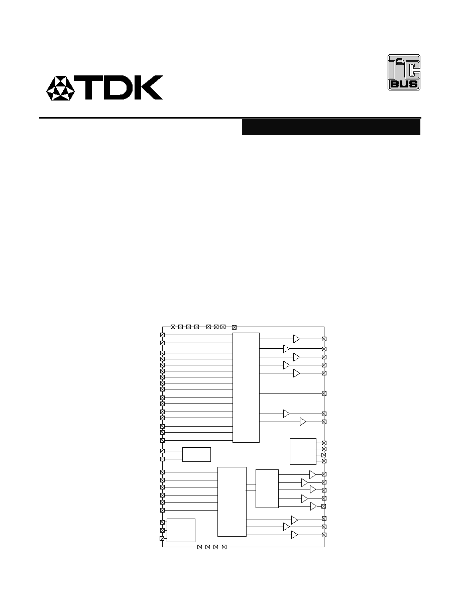
BLOCK DIAGRAM
Aux_Lin
Rin
Lin
TV_Rin
TV_Lin
Aux_Rin
Volume
Control
Mux
Rout
Lout
Aux_Mono
TV_Rout
TV_Lout
Aux_Rout
Aux_Lout
Serial
Port
SCLK
SDATA
Enc_B
Enc_G
Enc_R
Mux
Aux_YCout
Aux_B
Aux_G
Aux_R
Aux_YC
TV_B
TV_G
TV_R
TV_YCout
VC
C
GN
D
GN
D
GN
D
VE
E
EBLANK
ABLANK
BLANK
VC
C
GN
D
Enc_YC
Enc_Y
Enc_C
Aux_Fnc
VC
C
Other I/O
TV_Fnc
DO_0
DO_1
MOD_Mono
VE
E
Support
Circuits
Tgen
Rbias
Vref
VE
E
VC
C
VD
D
Enc2_Y
Enc2_C
TV_YCin
Aux_Cin
MOD_YC
Aux_Cout

AVPro
Æ
5002CL
Dual SCART A/V Switch
FUNCTIONAL DESCRIPTION
The 5002CL is an audio/video switching device. The
device integrates both audio and video drivers so that it
can directly drive the SCART interface. The use of a -5
volt supply eliminates the need for AC coupling
capacitors on the audio outputs and the SCART audio
inputs. Since the ≠5V supply biases the substrate of the
device, the supplies sequencing should be such that
the ≠5V supply turns on first and turns off last. All
programmable functions of the device are controlled
through a standard I
2
C serial interface and a set of
internal registers.
The device will interface to an external video encoder
that provides six video outputs. In addition, the 5002CL
includes two programmable digital outputs and
provides inputs for the TV SCART audio/video.
SCART VIDEO SWITCHING
The device is designed to accept video signals from an
auxiliary SCART connector, TV SCART connector, and
an external video encoder/DAC device. The devices
include a set of analog multiplexers that receive video
signals from these sources and allow routing of the
signals to the various video outputs. The video output
drivers have a nominal gain of 1.83 V/V to allow for a
series resistance of 62 ohms prior to the 75 ohm
termination. A block diagram of the video switching
function is provided in Figure 1. Details of the register
settings are provided in the section titled "Serial Port
Register Tables".
Enc_B
Enc_G
Enc_R
Aux_YCout
Aux_B
Aux_G
Aux_YC
TV_B
TV_G
TV_R
TV_YCout
EBLANK
ABLANK
BLANK
Enc_YC
Aux_Cout
Aux_R
Mod_YC
Enc_C
Enc_Y
TV_Fnc
Mux
VGen
Aux_Fnc
Comparator
0V
4V
Mux
Mux
Mux
Mux
Mux
Mux
Mux
Aux_Cin
TV_YCin
Gain
Mux
Enc2_Y
Enc2_C
Figure 1: 5002CL Video switching block diagram
2

AVPro
Æ
5002CL
Dual SCART A/V Switch
TV RGB OUTPUTS
The device accepts RGB video signals from two
sources. The Aux_R, Aux_G, Aux_B input pins are
typically connected to the auxiliary SCART connector.
The Enc_R, Enc_G, Enc_B input pins are connected to
the RGB outputs of an external video encoder device.
These outputs are used as a video source for the TV
SCART pins TV_R, TV_G, and TV_B. The RGB video
source is selected by setting the lower three (3) bits of
serial port Register 1. When these bits are set to
xxxxx000, the RGB source will be the encoder. When
these bits are set to xxxxx001, the source will be the
auxiliary port. The TV RGB outputs can be muted
independently from the TV composite outputs. Setting
Bit 6 of Register 1 low (0) will allow normal operation.
Setting Bit 6 high (1) will set the TV RGB outputs to the
blank level.
RGB Gain: The gain of the RGB outputs can be
adjusted to one of four different levels. Bits 4 and 5 in
Register 2 set the gain of the RGB output amplifiers
according to the following table:
Bit 5
Bit 4
RGB Amplifier Gain
0
0
1
1
0
1
0
1
Gain = 1.83 V/V = A
0
Gain = A
0
- 10%
Gain = A
0
- 20%
Gain = A
0
- 30%
DC Restore: The device will generate a DC restore level
on each video output based on timing referenced to a
horizontal sync pulse. When the sync pulse is detected,
the DC restore circuit will act to position the blank level
to 0.6 V at the respective video output load. The device
can be programmed to look for the horizontal sync pulse
on all of the RGB input pins or on the associated
composite video input pin (Aux_YC for the auxiliary port
or Enc_YC for the external encoder). Bit 7 of Register 1
determines the horizontal sync source. At power-up, this
bit defaults to a low (0) state, which programs the device
to look for sync detect on the RGB input signals. In this
mode, the device can detect a horizontal sync on any of
the three RGB input signals. When Bit 7 is set to a high
(1) state, the device will look for a sync detect from the
signal on either the Aux_YC or Enc_YC pin depending
on which source is selected.
Blanking: The signal on the Blank output pin is
determined by the state of two MSBs in Register 2
according to the following table:
Bit 7
Bit 6
Blank source
0
0
1
1
0
1
0
1
BLANK = ABLANK
BLANK = EBLANK
BLANK = 0V
BLANK = 4V @ IC output pin
The user must insure that the source of the Blank
output is the same as the source for the RGB outputs,
i.e. ABLANK is selected when the auxiliary RGB is
active and EBLANK is selected when the encoder RGB
is active.
TV COMPOSITE OUTPUT
The device provides inputs for two composite video
sources that can be switched to the TV SCART
composite video pin, TV_YCout. The Aux_YC input pin
is typically connected to the "Video In" pin on the
auxiliary SCART connector. The Enc_YC input pin is
typically connected to the "YC" or "CVBS" output from
the external video encoder device. Selection of the
video source for the TV composite output is
accomplished when the RGB video source is selected
(see the register tables).
TV SVHS OUTPUT MODE
The device supports SVHS video format. The SVHS
mode is selected for the TV SCART using the lower
three (3) bits of Register 1(except for SVHS Enc 4
mode). When the SVHS mode is selected, the
TV_YCout pin will provide the luminance signal output
from the selected source. The chroma output will be
provided on the TV_R pin. The video source for SVHS
mode can be either the auxiliary port or the encoder port.
When the auxiliary port is selected as the video source,
the video on Aux_R will be provided at the TV_R output
pin and the Aux_YC video will be provided at the
TV_YCout pin.
The device will support SVHS mode for four encoder
interface formats. The first encoder interface format
accepts chroma signals on the Enc_C pin and
luminance signals on the Enc_Y pin. This is designated
"SVHS, Enc 1" mode. The second format will receive
chroma information on the Enc_B pin and luminance
information on Enc_G. This format is designated
"SVHS, Enc 2". The third format will receive chroma
information from the Enc_R pin and luminance
information from the Enc_G pin. This mode is
designated "SVHS, Enc 3" on the serial port register
table. For these three modes, audio will come from the
Lin/Rin inputs. The fourth format is designated "SVHS
Enc 4". It is selected by setting register one to xx110xxx.
Chroma information is received on the Enc2_C input pin
and the luminance is received on the Enc2_Y input pin.
For this mode only, audio will come from the
TV_Lin/TV_Rin inputs, and the video will have chroma
output on Aux_Cout, and luminance output on
Aux_YCout.
When the SVHS mode is selected, the DC restore on
the TV_R pin will average to approximately 1.8 VDC at
the output pin. The DC restore circuit will act to position
the blank level to 0.6 V at the TV_YCout video output
3
AVPro
Æ
5002CL
Dual SCART A/V Switch
load. The TV_G and TV_B outputs will be set to 0 VDC
when the SVHS mode is active.
RF MODULATOR OUTPUT
The device provides an output, Mod_YC, to drive an
external RF modulator. The Mod_YC output is a unity
gain amplifier designed to drive a 1k load or higher.
When the device is operating in the RGB mode, the
signal on the Mod_YC output will follow the same
source as the TV_YCout output.
When the device is in the SVHS mode, the Mod_YC
output can be driven by several sources depending on
the SVHS video source. These various options are
detailed in the serial port register table.
One case that requires additional detail is the auxiliary
SVHS mode. In the SVHS mode, the Aux_YC video
input will only provide luminance information.
Composite video for the modulator output must be
generated by summing this luma information with the
chroma information from the auxiliary port. The input
pin labeled Aux_Cin is used for this purpose. The
Aux_Cin input pin is AC coupled to the same source
that provides the input signal to Aux_R. An internal
summing node combines the video signal on Aux_Cin
(chroma) with the video signal on Aux_YC (luma) to
generate a composite video signal. In the auxiliary
SVHS mode, this signal is provided at the Mod_YC pin.
TV COMPOSITE VIDEO MUTE
The TV composite video outputs can be muted by
programming the lower three (3) bits in Register 1. The
power-up default condition is xxxxx111, which sets the
TV composite video outputs to 0 VDC and switches the
TV audio outputs to Aux_Lin/Aux_Rin. Setting these
bits to xxxxx110 will also mute the TV composite video
outputs and switch the TV audio outputs to Lin/Rin.
AUXILIARY COMPOSITE OUTPUT
The auxiliary port includes a composite video output pin
(AUX_YCout) that is typically connected to the "Video
Out" pin on an auxiliary SCART connector. Bits 3-5 in
Register 1 determine the source for the AUX_YCout pin
as well as for the Aux_Cout pin. When these bits are
set to xx000xxx, the video source will be the Enc_B
input. When these bits are set to xx001xxx, the video
source will be the Enc_YC input. When these bits are
set to xx010xxx, the video source will be the TV_YCin
input.
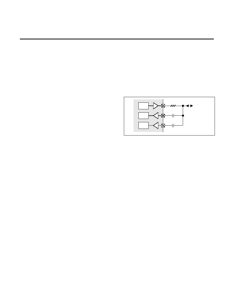
AUXILIARY SVHS OUTPUT MODE
In the SVHS mode, Pin 15 on the auxiliary SCART
connector provides chroma information. To support
this, the auxiliary port on the 5002CL includes a
chroma input pin (Aux_Cin) that is externally AC
coupled to Pin 15 on the auxiliary SCART connector.
The device also includes an output pin (Aux_Cout) that
provides a chroma output to Pin 15 (RED) on the
auxiliary SCART connector. When connected with the
Aux_R and Aux_Cin pins, this forms a bi-directional
port as shown in the following diagram:
Bi-Directional Pin Circuit
Using this configuration, the device will support SVHS
mode for four encoder interface formats. The first
encoder interface format will receive chroma information
from the Enc_C pin and luminance information from the
Enc_Y pin. This format is designated "SVHS, Enc 1".
The second format will receive chroma information on
the Enc_B input and luminance information on Enc_G.
This format is designated "SVHS, Enc 2". The third
format will receive chroma information from the Enc_R
pin and luminance information from the Enc_G pin. This
mode is designated "SVHS, Enc 3" on the serial port
register table. For these three modes, audio will come
from the Lin/Rin inputs. The fourth format is designated
"SVHS Enc 4". Chroma information is received on the
Enc2_C input pin and the luminance is received on the
Enc2_Y input pin. For this mode only, audio will come
from the TV_Lin/TV_Rin inputs.
Mux
Aux_R
Aux_Cout
Aux_Cin
62
Auxiliary
SCART
Pin 15
Mux
Mux
When the SVHS mode is selected, the DC restore on
the Aux_Cout pin will average to approximately 0.9
VDC at the video output load. The DC restore on the
Aux_YCout pin will set the blank level to 1.2 V at the IC
pin or approximately 0.6 V across the video output
load.
4
AVPro
Æ
5002CL
Dual SCART A/V Switch
AUXILIARY VIDEO MUTE
All auxiliary video outputs can be simultaneously disabled
by programming Bits 3-5 in Register 1. The power-up
default condition is xx111xxx, which sets all auxiliary video
outputs to 0 VDC and switches the auxiliary audio outputs
to Lin/Rin.
FUNCTION SWITCHING
The device provides functions switching pins for both the
Auxiliary (Aux_Fnc) and TV (TV_Fnc) SCART ports. Both of
these pins are bi-directional. The direction of the pins is
determined by setting bits in Register 2 according to the
following table:
Bits
Aux_Fnc
TV_Fnc
xxxx00xx
output
output
xxxx01xx
output
input
xxxx10xx
input
output
xxxx11xx
Passthru I/O
Passthru O/I
For the case where Register 2 is set to xxxx11xx, the input
signal on the Aux_Fnc pin is passed directly through to the
TV_Fnc pin as an output, or vice versa. This mode is
useful when the rest of the system powers down and all
signals from the auxiliary port are passed directly through to
the TV port, or vice versa.
When a function pin is set as an input, the voltage on that pin
is applied to an internal comparator. The comparator senses
the voltage on the input pin and sets the two (2) LSBs in the
read register according to the following table:
Input voltage
Bits
Function
< 2.0 V
xxxxxx00
Normal TV
4.5 to 7.0V
xxxxxx01
16:9 aspect
>9.5 V
xxxxxx10
Peritelevision
When a function pin is set as an output, the output level
for the pin is determined by the state of the two LSBs in
Register 2, according to the following table:
Bits
Output voltage
Function
xxxxxx00
~0 V
Normal TV
xxxxxx01
~6 V
16:9 aspect
xxxxxx10
~ 11 V
Peritelevision
xxxxxx11
~ 11 V
Peritelevision
Note that both the Aux_Fnc pin and the TV_Fnc pin can
be set as outputs simultaneously, however they will have
the same output voltage.
The function output circuit includes short circuit protection.
When a function pin is in the 6V or 11V output mode, if the
SCART connection is shorted to ground, then the output is
disabled. Likewise, when a function pin is in the 0V output
mode, if the SCART connection is connected to a voltage
source, then the output is disabled. The load for the
function outputs is designed to be 10k or higher.
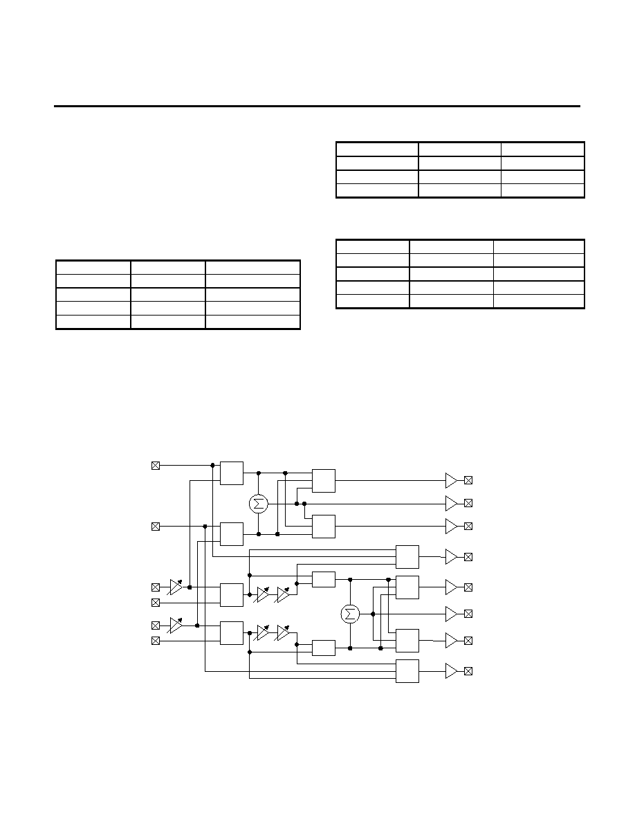
Figure 2: 5002CL Audio Switching Block Diagram
Aux_Rin
Aux_Lout
Mux
Aux_Rout
Aux_Mono
Mux
Mux
Mux
Aux_Lin
Lin
Rin
Mux
Mux
TV_Rin
TV_Lin
Lout
TV_Lout
Mux
Mux
Mux
Mux
TV_Rout
Rout
Mux
Mux
Mod_Mono
A
B
C
A
B
C
A: DAC Input Gain (0, 6, 9, or 11.6dB)
B: Volume Control Gain (0 or 6dB)
C: Volume Control Attenuation (0 to ≠31 dB in ≠1dB steps)
5