73K324L
CCITT V.22bis, V.22, V.21, V.23, Bell 212A
Single-Chip Modem
June 2001
DESCRIPTION
The 73K324L is a highly integrated single-chip
modem IC which provides the functions needed to
design a Quad-mode CCITT and Bell 212A
compatible modem capable of operation over dial-up
lines. The 73K324L adds V.23 capability to the
CCITT modes of TDK Semiconductor Corporation's
73K224 one-chip modem, allowing a one-chip
implementation in designs intended for European
markets which require this added Modulation mode.
The 73K324L offers excellent performance and a
high level of functional integration in a single IC. The
device supports V.22bis, V.22, Bell 212A, V.21, and
V.23 operating modes, allowing both synchronous
and asynchronous operation as defined by the
appropriate standard.
The 73K324L is designed to appear to the Systems
Engineer as a microprocessor peripheral, and will
easily interface with popular one-chip
microcontrollers (80C51 typical) for control of
modem functions through its 8-bit multiplexed
address/data bus. A serial control bus is available
for applications not requiring a parallel interface. An
optional package with only the serial control bus is
also available. Data communications occurs through
a separate serial port.
(continued)
FEATURES
∑ One chip Multi-mode CCITT V.22bis, V.22, V.21,
V.23 and Bell 212A compatible modem data pump
∑ FSK (75, 300, 1200 bit/s), DPSK (600, 1200 bit/s),
or QAM (2400 bit/s) encoding
∑ Pin and software compatible with other
TDK Semiconductor Corporation K-Series family
one-chip modems
∑ Interfaces directly with standard
microprocessors (8048, 80C51 typical)
∑ Serial and parallel microprocessor bus for
control
∑ Selectable asynch/synch with internal
buffer/debuffer and scrambler/descrambler
functions
∑ All synchronous (internal, external, slave) and
Asynchronous Operating modes
∑ Adaptive equalization for optimum performance
over all lines
∑ Programmable transmit attenuation (16 dB, 1 dB
steps), and selectable receive boost (+18 dB)
∑ Call progress, carrier, answer tone, unscrambled
mark, S1, and signal quality monitors
∑ DTMF, answer, calling, SCT and guard tone
generators
∑ Test modes available: ALB, DL, RDL; Mark, Space
and Alternating bit pattern generators
∑ CMOS technology for low power consumption
(100 MW @ 5 V) with power-down mode
(15 mW @ 5V)
∑ 4-wire full duplex operation in all modes
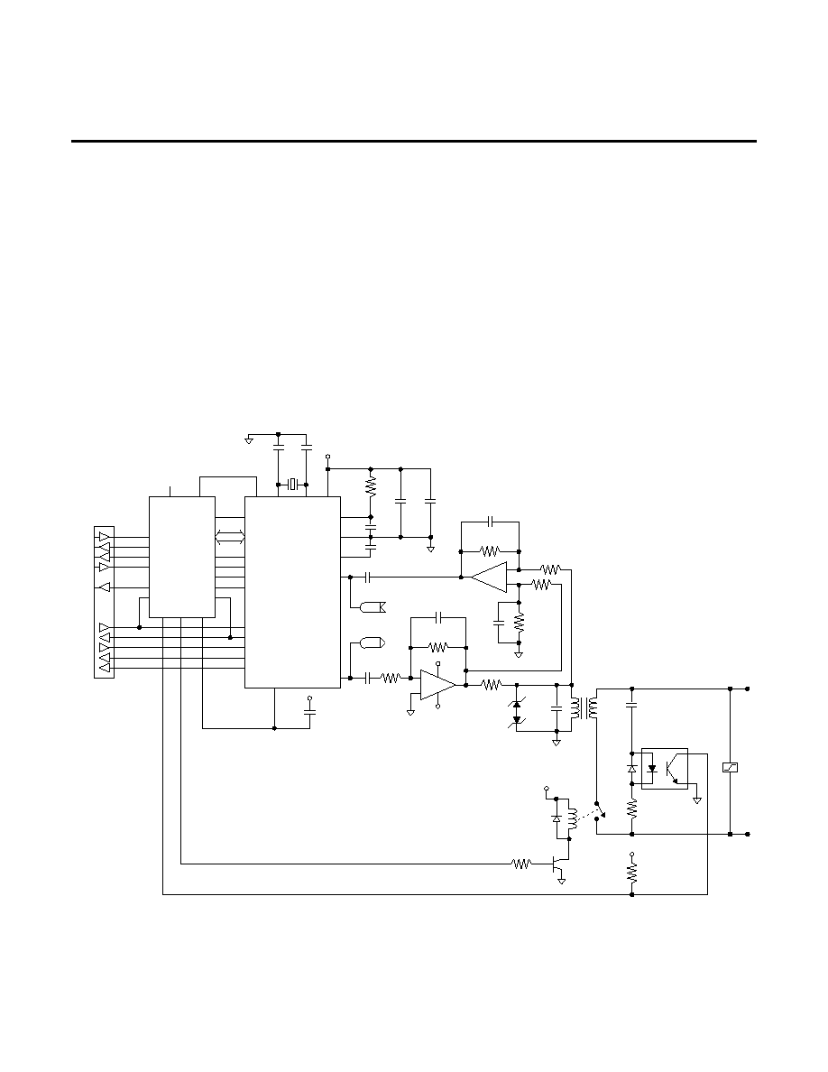
BLOCK DIAGRAM
TDK SEMICONDUCTOR CORP.
Æ
DIGITAL
SIGNAL
PROCESSOR
RECEIVE
FUNCTIONS
DI-BIT/
QUAD-BIT
DECODER
T X D
RXD
SERIAL
INTERFACE
BUFFER
8-BIT
µP
BUS
INTERFACE
DEBUFFER
EQUALIZER
FILTER
FILTER
T X A 1
RXA
P A S S
BAND
FILTER
EQUALIZER
FILTER
FIXED
DEMODULATOR
6dB
GAIN
BOOST
6dB
GAIN
BOOST
6dB
GAIN
BOOST
ATTENUATOR
TONE
DETECTION
FIR
PULSE
SHAPER
QAM/
DPSK
MODULATOR
DI-BIT/
QUAD-BIT
ENCODER
FSK
MODULATOR
SCRAMBLER
DTMF,
ANSWER,
GUARD &
CALLING
TONE
GENERATOR
DESCRAMBLER
A/D
ANTI-ALIAS
FILTER

73K324L
CCITT V.22bis, V.22, V.21, V.23, Bell 212A
Single-Chip Modem
2
DESCRIPTION
(continued)
The 73K324L offers full hardware and software
compatibility with other products in TDK
Semiconductor's K-Series family of single-chip
modems, allowing system upgrades with a single
component change. The 73K324L is ideal for use in
free-standing or integral system modem products
where full-duplex 2400 bit/s operation with Alternate
mode capability is required. Its high functionality, low
power consumption, and efficient packaging simplify
design requirements and increase system reliability.
A complete modem requires only the addition of the
phone line interface, a control microprocessor, and
RS-232 level converters for a typical system.
The 73K324L is designed to provide a complete
V.22bis, V.22, Bell 212A, V.21, and V.23 compatible
modem on a chip. Many functions were included to
simplify implementation in typical modem designs. In
addition to the basic 2400 bit/s QAM, 1200/600 bit/s
DPSK and 1200/300/75 bit/s FSK
modulator/demodulator sections, the device also
includes synch/asynch buffering, DTMF, answer,
soft carrier, guard, and calling tone generator
capabilities. Handshake pattern detectors simplify
control of connect sequences, and precise tone
detectors allow accurate detection of call progress,
answer, calling, and soft carrier turn off tones. All
Operating modes defined by the incorporated
standards are included, and Test modes are
provided. Most functions are selectable as options,
and logical defaults are provided. The device can be
directly interfaced to a microprocessor via its 8-bit
multiplexed address/data bus for control and status
monitoring. Data communications takes place
through a separate serial port. Data may also be
sent and received through the control registers. This
simplifies designs requiring speed buffering, error
control and compression.
FUNCTIONAL DESCRIPTION
QAM MODULATOR/DEMODULATOR
The 73K324L encodes incoming data into quad-bits
represented by 16 possible signal points with
specific phase and amplitude levels. The baseband
signal is then filtered to reduce intersymbol
interference on the bandlimited telephone network.
The modulator transmits this encoded data using
either a 1200 Hz (Originate mode) or 2400 Hz
(Answer mode) carrier. The demodulator, although
more complex, essentially reverses this procedure
while also recovering the data clock from the
incoming signal. Adaptive equalization corrects for
varying line conditions by automatically changing
filter parameters to compensate for line
characteristics.
DPSK MODULATOR/DEMODULATOR
The 73K324L modulates a serial bit stream into
di-bit pairs that are represented by four possible
phase shifts as prescribed by the Bell 212A/V.22
standards. The baseband signal is then filtered to
reduce intersymbol interference on the bandlimited
2-wire PSTN line. Transmission occurs on either a
1200 Hz (Originate mode) or 2400 Hz carrier
(Answer mode). Demodulation is the reverse of the
modulation process, with the incoming analog signal
eventually decoded into di-bits and converted back
to a serial bit stream. The demodulator also recovers
the clock, which was encoded into the analog signal
during modulation. Demodulation occurs using either
a 1200 Hz carrier (Answer mode or ALB Originate
mode) or a 2400 Hz carrier (Originate mode or ALB
Answer mode). The 73K324L use a phase locked
loop coherent demodulation technique that offers
excellent performance. Adaptive equalization is also
used in DPSK modes for optimum operation with
varying lines.
FSK MODULATOR/DEMODULATOR
The FSK modulator/demodulator produces a
frequency modulated analog output signal using two
discrete frequencies to represent the binary data.
V.21 frequencies of 980 and 1180 Hz (originate
mark and space), or 1650 and 1850 Hz (answer
mark and space) are used in V.21 mode. V.23 mode
uses 1300 and 2100 Hz for the main channel or 390
and 450 Hz for the back channel. Demodulation
involves detecting the received frequencies and
decoding them into the appropriate binary value.
The rate converter and scrambler/descrambler are
automatically bypassed in the FSK modes.
PASSBAND FILTERS AND EQUALIZERS
High and low band filters are included to shape the
amplitude and phase response of the transmit and
receive signals and to provide compromise delay
equalization as well as rejection of out-of-band
signals. The transmit signal filtering corresponds to a
&%% raised cosine frequency response
characteristic.

73K324L
CCITT V.22bis, V.22, V.21, V.23, Bell 212A
Single-Chip Modem
3
ASYNCHRONOUS MODE
The Asynchronous mode is used for communication
with asynchronous terminals which may transfer
data at 600, 1200, or 2400 bit/s +1%, -2.5% even
though the modem's output is limited to the nominal
bit rate ±0.01% in DPSK and QAM modes. When
transmitting in this mode the serial data on the TXD
input is passed through a rate converter which
inserts or deletes stop bits in the serial bit stream in
order to output a signal that is the nominal bit rate
±0.01%. This signal is then routed to a data
scrambler and into the analog modulator where di-bit
or quad-bit encoding results in the output signal.
Both the rate converter and scrambler can be
bypassed for handshaking and synchronous
operation as selected. Received data is processed
in a similar fashion except that the rate converter
now acts to reinsert any deleted stop bits and output
data to the terminal at no greater than the bit rate
plus 1%. An incoming break signal (low through two
characters) will be recognized and passed through
without incorrectly inserting a stop bit.
The SYNC/ASYNC converter has an extended
Overspeed mode which allows selection of an output
speed range of either +1% or +2.3%. In the
extended Overspeed mode, some stop bits are
output at 7/8 the normal width.
Both the SYNC/ASYNC rate converter and the data
descrambler are automatically bypassed in the FSK
modes.
SYNCHRONOUS MODE
Synchronous operation is possible only in the QAM
or DPSK modes. Operation is similar to that of the
Asynchronous mode except that data must be
synchronized to a clock and no variation in data
transfer rate is allowable. Serial input data appearing
at TXD must be valid on the rising edge of TXCLK.
TXCLK is an internally derived 1200 or 2400 Hz
signal in Internal mode and is connected internally to
the RXCLK pin in Slave mode. Receive data at the
RXD pin is clocked out on the falling edge of
RXCLK. The asynch/synch converter is bypassed
when Synchronous mode is selected and data is
transmitted out at essentially the same rate as it is
input.
PARALLEL CONTROL INTERFACE
Eight 8-bit registers are provided for control, option
select, and status monitoring. These registers are
addressed with the AD0, AD1, and AD2 multiplexed
address lines (latched by ALE) and appear to a
control microprocessor as seven consecutive
memory locations. Six control registers are
read/write. The detect and ID registers are read only
and cannot be modified except by modem response
to monitored parameters.
SERIAL CONTROL INTERFACE
The Serial Command mode allows access to the
73K324L control and status registers via a serial
control port. In this mode the A0, A1, and A2 lines
provide register addresses for data passed through
the DATA pin under control of the
RD and WR lines.
A read operation is initiated when the
RD line is
taken low. The next eight cycles of EXCLK will then
transfer out eight bits of the selected addresss
location LSB first. A write takes place by shifting in
eight bits of data LSB first for eight consectuive
cycles of EXCLK.
WR is then pulsed low and data
transfer into the selected register occurs on the
rising edge of
WR.
TONE GENERATOR
The DTMF generator controls the sending of the
sixteen standard DTMF tone pairs. The tone pair
sent is determined by selecting TRANSMIT DTMF
(bit D4) and the 4 DTMF bits (D0-D3) of the TONE
register. Transmission of DTMF tones from TXA is
gated by the TRANSMIT ENABLE bit of CR0 (bit D1)
as with all other analog signals.
FULL DUPLEX OPERATION
Four-wire full duplex operation is allowed in all
modes. This feature allows transmission and
reception in the same band for four wire applications
only.

73K324L
CCITT V.22bis, V.22, V.21, V.23, Bell 212A
Single-Chip Modem
4
PIN DESCRIPTION
POWER
NAME TYPE
DESCRIPTION
GND I
System
Ground.
VDD
I
Power supply input, 5V -5% +10%. Bypass with 0.22 µF and 22 µF capacitors to
GND.
VREF
O
An internally generated reference voltage. Bypass with 0.22 µF capacitor to GND.
ISET
I
Chip current reference. Sets bias current for op-amps. The chip current is set by
connecting this pin to VDD through a 2 M
resistor. Iset should be bypassed to
GND with a 0.22 µF capacitor.
PARALLEL MICROPROCESSOR INTERFACE
ALE
I
Address latch enable. The falling edge of ALE latches the address on AD0-AD2
and the chip select on
CS.
AD0- AD7
I/O /
Tristate
Address/data bus. These bidirectional tri-state multi-plexed lines carry information
to and from the internal registers.
CS
I
Chip select. A low on this pin allows a read cycle or a write cycle to occur. AD0-
AD7 will not be driven and no registers will be written if
CS (latched) is not active.
CS is latched on the falling edge of ALE.
CLK
O
Output clock. This pin is selectable under processor control to be either the crystal
frequency (for use as a processor clock) or 16 x the data rate for use as a baud
rate clock in QAM/DPSK modes only. The pin defaults to the crystal frequency on
reset.
INT
O
Interrupt. This open drain weak pullup, output signal is used to inform the
processor that a detect flag has occurred. The processor must then read the detect
register to determine which detect triggered the interrupt.
INT will stay active until
the processor reads the detect register or does a full reset.
RD
I
Read. A low requests a read of the 73K324L internal registers. Data cannot be
output unless both
RD and the latched CS are active or low.
RESET
I
Reset. An active high signal on this pin will put the chip into an inactive state. All
control register bits (CR0, CR1, CR2, CR3, Tone) will be reset. The output of the
CLK pin will be set to the crystal frequency. An internal pull down resistor permits
power on reset using a capacitor to VDD.
WR
I
Write. A low on this informs the 73K324L that data is available on AD0-AD7 for
writing into an internal register. Data is latched on the rising edge of
WR. No data
is written unless both
WR and the latched CS are low.
NOTE: The Serial Control mode is provided by tying ALE high and
CS low. In this configuration AD7 becomes
DATA and AD0, AD1 and AD2 become the address only. See the serial time diagrams on page 23.

73K324L
CCITT V.22bis, V.22, V.21, V.23, Bell 212A
Single-Chip Modem
5
RS-232 INTERFACE
NAME TYPE
DESCRIPTION
EXCLK
I
External Clock. This signal is used in synchronous transmission when the external
timing option has been selected. In the External Timing mode the rising edge of
EXCLK is used to strobe synchronous transmit data available on the TXD pin. Also
used for serial control interface.
RXCLK
O/Tristate Receive Clock Tri-statable. The falling edge of this clock output is coincident with
the transitions in the serial received DPSK/QAM data output. The rising edge of
RXCLK can be used to latch the valid output data. RXCLK will be valid as long as
a carrier is present. In V.23 or V.21 mode a clock which is 16 x 1200/75 or 16 x
300 Hz data rate is output, respectively.
RXD O/
Weak
Pull-up
Received Data Output. Serial receive data is available on this pin. The data is
always valid on the rising edge of RXCLK when in Synchronous mode. RXD will
output constant marks if no carrier is detected.
TXCLK
O/Tristate Transmit Clock Tri-statable. This signal is used in synchronous DPSK/QAM
transmission to latch serial input data on the TXD pin. Data must be provided so
that valid data is available on the rising edge of the TXCLK. The transmit clock is
derived from different sources depending upon the Synchronization mode
selection. In Internal Mode the clock is generated internally (2400 Hz for QAM,
1200 Hz for DPSK or 600 Hz for half-speed DPSK). In External Mode TXCLK is
phase locked to the EXCLK pin. In Slave Mode TXCLK is phase locked to the
RXCLK pin. TXCLK is always active. In V.23 or V.21 mode the output is a 16 x
1200/75 or 16 x 300 Hz clock, respectively.
TXD
I
Transmit Data Input. Serial data for transmission is input on this pin. In
Synchronous modes, the data must be valid on the rising edge of the TXCLK
clock. In Asynchronous modes (2400/1200/600 bit/s, or 75/300 baud) no clocking
is necessary. DPSK/QAM data must be +1%, -2.5% or +2.3%, -2.5 % in Extended
Overspeed mode.
ANALOG INTERFACE
RXA
I
Received modulated analog signal input from the phone line.
TXA
O
Transmit analog output to the phone line.
XTL1 I
XTL2 I/O
These pins are for the internal crystal oscillator requiring a 11.0592 MHz Parallel
mode crystal. Two capacitors from these pins to ground are also required for
proper crystal operation. Consult crystal manufacturer for proper values. XTL2 can
also be driven from an external clock.

73K324L
CCITT V.22bis, V.22, V.21, V.23, Bell 212A
Single-Chip Modem
6
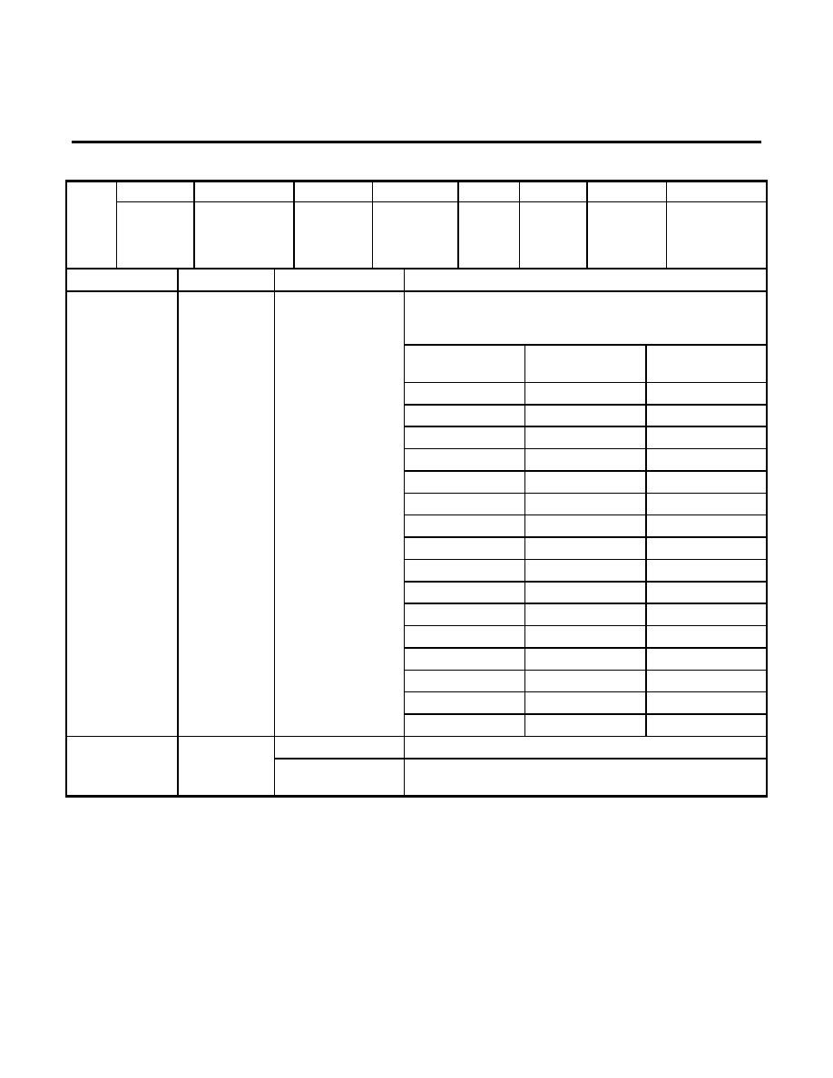
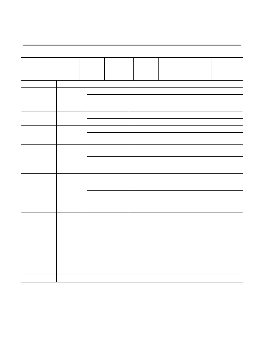
REGISTER DESCRIPTIONS
Eight 8-bit internal registers are accessible for
control and status monitoring. The registers are
accessed in read or write operations by addressing
the A0, A1 and A2 address lines in Serial mode, or
the AD0, AD1 and AD2 lines in Parallel mode. The
address lines are latched by ALE. Register CR0
controls the method by which data is transferred
over the phone line. CR1 controls the interface
between the microprocessor and the 73K324L
internal state. DR is a detect register which provides
an indication of monitored modem status conditions.
TR, the tone control register, controls the DTMF
generator, answer, guard tones, SCT, calling tone,
and RXD output gate used in the modem initial
connect sequence. CR2 is the primary DSP control
interface and CR3 controls transmit attenuation and
receive gain adjustments. All registers are read/write
except for DR and ID which are read only. Register
control and status bits are identified below:
REGISTER BIT SUMMARY
NOTE: When a register containing reserved control bits is written into, the reserved bits must be programmed as
0's.
X = Undefined, mask in software.
DTMF0/GUARD/
ANSWER/
CALLING/SCT
REGISTER
CONTROL
REGISTER
0
ID
REGISTER
SPECIAL
REGISTER
CONTROL
REGISTER
1
DETECT
REGISTER
TONE
CONTROL
REGISTER
CONTROL
REGISTER
2
ID
SR
CR2
CR1
DR
TR
ADDRESS
AD - A0
110
101
100
011
010
001
000
D7
TRANSMIT
PATTERN
1
TRANSMIT
PATTERN
0
RXD
OUTPUT
CONTROL
D6
D5
ENABLE
DETECT
INTERRUPT
RECEIVE
DATA
TRANSMIT
ANSWER
TONE
TRANSMIT
MODE
2
TRANSMIT
DTMF
TRANSMIT
MODE
1
CLK
CONTROL
CARRIER
DETECT
DTMF3
DTMF1/
OVERSPEED
TRANSMIT
MODE
0
RESET
SPECIAL
TONE
DETECT
DTMF2/
4 WIRE FDX
TRANSMIT
ENABLE
TEST
MODE
1
CALL
PROGRESS
DETECT
ANSWER/
ORIGINATE
TEST
MODE
0
SIGNAL
QUALITY
D4
D3
D2
D1
D0
DATA BIT NUMBER
CR0
MODULATION
OPTION
1
1
TRANSMIT
GUARD TONE/
SCT/CALLING
TONE
BYPASS
SCRAMBLER/
ADD PH. EQ.
(V.23)
RECEIVE
LEVEL
0
TX BAUD
CLOCK
SPECIAL
REGISTER
ACCESS
1
RX UNSCR.
DATA
PATTERN
S1 DET
MODULATION
TYPE
1
MODULATION
TYPE
0
CALL
INITIALIZE
UNSCR.
MARK
DETECT
TRANSMIT
S1
TXD
SOURCE
SQ
SELECT 1
SQ
SELECT 0
16 WAY
RESET
DSP
TRAIN
INHIBIT
EQUALIZER
ENABLE
CONTROL
REGISTER
3
CR3
101
TXDALT
TRISTATE
TX/RXCLK
0
RECEIVE
GAIN
BOOST
TRANSMIT
ATTEN.
3
TRANSMIT
ATTEN.
2
TRANSMIT
ATTEN.
1
TRANSMIT
ATTEN.
0
0
0
0
0
X
X
X
X

73K324L
CCITT V.22bis, V.22, V.21, V.23, Bell 212A
Single-Chip Modem
7
REGISTER ADDRESS TABLE
00=NORMAL
01=ANALOG LOOPBACK
10=REMOTE DIGITAL
LOOPBACK
11=LOCAL DIGITAL
LOOPBACK
CONTROL
REGISTER
0
000
TRANSMIT
MODE
2
TRANSMIT
MODE
1
TRANSMIT
ENABLE
ANSWER/
ORIGINATE
DATA BIT NUMBER
AD2 - AD0
REGISTER
ADDRESS
D7
D6
D5
D4
D3
D2
D1
D0
TEST
MODE
0
TEST
MODE
1
RESET
CLK
CONTROL
BYPASS
SCRAMBLER/
ADD PH. EQ.
(V.23)
ENABLE
DETECT
INTERRUPT
TRANSMIT
PATTERN
0
TRANSMIT
PATTERN
1
001
CONTROL
REGISTER
1
CR1
SIGNAL
QUALITY
INDICATOR
CP
TONE
DETECT
SPECIAL
TONE
DETECT
CARRIER
DETECT
UNSCR.
MARKS
DETECT
RECEIVE
DATA
010
DETECT
REGISTER
DR
TRANSMIT
MODE
0
0000=PWR DOWN
0001=INT SYNCH
0010=EXT SYNCH
0011=SLAVE SYNCH
0100=ASYCH 8 BITS/CHAR
0101=ASYCH 9 BITS/CHAR
0110=ASYCH 10 BITS/CHAR
0111=ASYCH 11 BITS/CHAR
1X00=FSK
0=DISABLE
TXA OUTPUT
1=ENABLE
TXA OUTPUT
0=ANSWER
1=ORIGINATE
in V.23
0=BC xmit
1=MC xmit
00=TX DATA
01=TX ALTERNATE
10=TX MARK
11=TX SPACE
0=OFF
1=ON
0=NORMAL
1=BYPASS
SCRAMBLER
0=XTAL
1=16 X DATA
RATE OUTPUT
AT CLK PIN IN
QAM/DPSK
MODE ONLY
0=NORMAL
1=RESET
OUTPUTS
RECEIVED
DATA STREAM
0=CONDITION NOT DETECTED
1=CONDITION DETECTED
CR0
MODULATION
OPTION
0=2400 BIT/S
0=1200 BIT/S
1=600 BIT/S
0=V.23
1=V.21
MODULATION
TYPE
1
MODULATION
TYPE
0
10=QAM
00=DPSK
01=FSK
RECEIVE
LEVEL
INDICATOR
S1 PATTERN
DETECT
0=SIGNAL
BELOW
THRESHOLD
1=ABOVE
THRESHOLD
0=GOOD
1=BAD
DTMF0/
GUARD/
ANSWER/
CALLING/SCT
DTMF1/
OVERSPEED
DTMF2/
4 WIRE
FDX
DTMF3
TRANSMIT
DTMF
TRANSMIT
ANSWER
TONE
RXD
OUTPUT
CONTROL
011
TONE
CONTROL
REGISTER
TR
RXD PIN
0=NORMAL
1=TRI-STATE
0=OFF
1=ON
1=TX DTMF
4 BIT CODE FOR 1 OF 16
DUAL TONE COMBINATIONS
TRANSMIT
GUARD/
CALLING/
SCT TONE
GUARD:
ANSWER:
CALLING:
SCT:
0=OFF
1=ON
EQUALIZER
ENABLE
TRAIN
INHIBIT
RESET
DSP
16 WAY
TRANSMIT
S1
CALL
INITIALIZE
100
CONTROL
REGISTER
2
CR2
0=DSP IN
DEMOD MODE
1=DSP IN CALL
PROGRESS
MODE
0=NORMAL
DOTTING
1=S1
TRANSMIT
ATTEN.
0
RECEIVE
GAIN
BOOST
101
CONTROL
REGISTER
3
CR3
0=NO BOOST
1=18 dB BOOST
0000-1111, SETS
TRANSMIT ATTENUATOR
16 dB RANGE
DEFAULT=0100 ≥ -10 dbM0
0=RX=TX
1=RX=16 WAY
0=DSP
INACTIVE
1=DSP
ACTIVE
0=ADAPT EQ
ACTIVE
1=ADAPT EQ
FROZEN
0=ADAPT EQ
IN INIT
1=ADAPT EQ
OK TO ADAPT
TRANSMIT
ATTEN.
2
TRANSMIT
ATTEN.
1
TRANSMIT
ATTEN.
3
QAM:
DPSK:
FSK:
0=NOT PRESENT
1=PATTERN
FOUND
0=NORMAL OPERATION
1=ALLOWS V.23 FULL
DUPLEX OPERATION
SPECIAL
REGISTER
ACCESS
0=ACCESS CR3
1=ACCESS
SPECIAL
REGISTER
TXDALT
TRISTATE
TX/RXCLK
0=CLOCK
DRIVEN
1=CLOCK
TRISTATE
SPECIAL
REGISTER
101
TX BAUD
CLOCK
RX UNSCR.
DATA
TXD
SOURCE
SQ
SELECT1
SQ
SELECT0
OUTPUTS
TXBAUD
CLOCK
OUTPUTS
UNSCR.
DATA
0=TXD PIN
1=TX DATA
CR3-D7
00≥10 BER
-5
01≥10 BER
-6
10≥10 BER
-4
11≥10 BER
-3
ALTERNATE
TRANSMIT
DATA
SOURCE
SR
MUST BE 0
0
0 - 1800 HZ
1 - 550 HZ
0 - 2225 HZ
1 - 2100 HZ
0 - 1300 HZ
1 - 900 HZ
00XX=73K212AL, 322L, 321L
01XX=73K221AL, 302L
10XX=73K222AL, 222BL
1100=73K224L
1110=73K324L
1100=73K224BL
1110=73K324BL
ID
REGISTER
10
110
1
1
1
0
0
0
0
X
X
X
X

73K324L
CCITT V.22bis, V.22, V.21, V.23, Bell 212A
Single-Chip Modem
8
CONTROL REGISTER 0
D7 D6 D5 D4 D3 D2 D1 D0
CR0
000
MODUL.
OPTION
MODUL.
TYPE 1
MODUL.
TYPE 0
TRANSMIT
MODE 2
TRANSMIT
MODE 1
TRANSMIT
MODE 0
TRANSMIT
ENABLE
ANSWER/
ORIGINATE
BIT NO.
NAME
CONDITION
DESCRIPTION
0
Selects Answer mode (transmit in high band, receive in
low band) or in V.23 HDX mode, receive at 1200 bit/s and
transmit at 75 bit/s.
1
Selects Originate mode (transmit in low band,receive in
high band) or in V.23 HDX mode, receive at 75 bit/s and
transmit at 1200 bit/s.
D0 Answer/
Originate
Note: This bit works with Tone Register bits D0 and D6 to
program special tones detected in the Detect Register.
See Detect and Tone Registers.
0
Disables transmit output at TXA.
1
Enables transmit output at TXA.
D1 Transmit
Enable
Note: Transmit Enable must be set to 1 to allow activation
of Answer Tone, DTMF, or Carrier.
D5 D4 D3 D2
0
0 0 0
Selects Power Down mode. All functions are disabled
except the digital interface.
0
0 0
1
Internal Synchronous mode. In this mode TXCLK is an
internally derived 600, 1200 or 2400 Hz signal. Serial
input data appearing at TXD must be valid on the rising
edge of TXCLK. Receive data is clocked out of RXD on
the falling edge of RXCLK.
0 0 1 0 External Synchronous mode. Operation is identical to
internal synchronous, but TXCLK is connected internally
to EXCLK pin, and a 600, 1200 or 2400 Hz clock must be
supplied externally.
0 0 1 1 Slave Synchronous mode. Same operation as other
Synchronous modes. TXCLK is connected internally to
the RXCLK pin in this mode.
0
1
0
0
Selects Asynchronous mode - 8 bits/character (1 start bit,
6 data bits, 1 stop bit).
0
1
0
1
Selects Asynchronous mode - 9 bits/character (1 start bit,
7 data bits, 1 stop bit).
0
1 1
0
Selects Asynchronous mode - 10 bits/character (1 start
bit, 8 data bits, 1 stop bit).
0
1 1
1
Selects Asynchronous mode - 11 bits/character (1 start
bit, 8 data bits, Parity and/or 1 or 2 stop bits).
D5, D4,
D3, D2
Transmit
Mode
1
X
0
0
Selects FSK operation.

73K324L
CCITT V.22bis, V.22, V.21, V.23, Bell 212A
Single-Chip Modem
9
CONTROL REGISTER 0
(continued)
BIT NO.
NAME
CONDITION
DESCRIPTION
D6 D5
1 0
QAM
0 0
DPSK
D6,D5 Modulation
Type
0 1
FSK
0
QAM selects 2400 bit/s. DPSK selects 1200 bit/s.
FSK selects V.23 mode.
D7 Modulation
Option
1
DPSK selects 600 bit/s.
FSK selects V.21 mode.
CONTROL REGISTER 1
D7 D6 D5 D4 D3 D2 D1 D0
CR1
001
TRANSMIT
PATTERN
1
TRANSMIT
PATTERN
0
ENABLE
DETECT
INT.
BYPASS
SCRAMB/
ADD
PH.EQ
CLK
CONTROL
RESET TEST
MODE
1
TEST
MODE
0
BIT NO.
NAME
CONDITION
DESCRIPTION
D1 D0
0 0
Selects Normal Operating mode.
0
1
Analog Loopback mode. Loops the transmitted analog
signal back to the receiver, and causes the receiver to
use the same carrier frequency as the transmitter. To
squelch the TXA pin, transmit enable bit must be low.
Tone Register bit D2 must be zero.
1
0
Selects remote digital loopback. Received data is looped
back to transmit data internally, and RXD is forced to a
mark. Data on TXD is ignored.
D1, D0
Test Mode
1
1
Selects local digital loopback. Internally loops TXD back to
RXD and continues to transmit data carrrier at TXA pin.
0
Selects normal operation.
D2 Reset
1
Resets modem to power down state. All control register
bits (CR0, CR1, CR2, CR3 and Tone) are reset to zero
except CR3 bit D2. The output of the clock pin will be set
to the crystal frequency.
0
Selects 11.0592 MHz crystal echo output at CLK pin.
D3 CLK
Control
(Clock Control)
1
Selects 16 X the data rate output at CLK pin in QAM and
DPSK only.
73K324L
CCITT V.22bis, V.22, V.21, V.23, Bell 212A
Single-Chip Modem
10
CONTROL REGISTER 1
(continued)
D7 D6 D5 D4 D3 D2 D1 D0
CR1
001
TRANSMIT
PATTERN
1
TRANSMIT
PATTERN
0
ENABLE
DETECT
INT.
BYPASS
SCRAMB/
ADD
PH.EQ.
CLK
CONTROL
RESET TEST
MODE
1
TEST
MODE
0
BIT NO.
NAME
CONDITION
DESCRIPTION
0
Selects normal operation. DPSK and QAM data is
passed through scrambler.
D4 Bypass
Scrambler/
Add Ph. Eq.
1
Selects Scrambler Bypass. DPSK and QAM data is
routed around scrambler in the transmit path. In the V.23
mode, additional phase equalization is added to the main
channel filters when D4 is set to 1.
0
Disables interrupt at
INT pin. All interrupts are normally
disabled in Power Down mode.
D5 Enable
Detect
Interrupt
1 Enables
INT output. An interrupt will be generated with a
change in status of DR bits D1-D4 and D6. The answer
tone and call progress detect interrupts are masked when
the TX enable bit is set. Carrier detect is masked when
TX DTMF is activated. All interrupts will be disabled if the
device is in Power Down mode.
D7 D6
0 0
Selects normal data transmission as controlled by the
state of the TXD pin.
0
1
Selects an alternating mark/space transmit pattern for
modem testing and handshaking. Also used for S1
pattern generation. See CR2 bit D4.
1
0
Selects a constant mark transmit pattern.
D7, D6
Transmit
Pattern
1
1
Selects a constant space transmit pattern.
73K324L
CCITT V.22bis, V.22, V.21, V.23, Bell 212A
Single-Chip Modem
11
DETECT REGISTER
D7 D6 D5 D4 D3 D2 D1 D0
DR
010
RECEIVE
LEVEL
INDICATOR
S1
PATTERN
DETECT
RECEIVE
DATA
UNSCR.
MARK
DETECT
CARRIER
DETECT
SPECIAL
TONE
DETECT
CALL
PROG.
DETECT
SIGNAL
QUALITY
INDICATOR
BIT NO.
NAME
CONDITION
DESCRIPTION
0
Indicates normal received signal.
D0 Signal
Quality
Indicator
1
Indicates low received signal quality (above average error
rate). Interacts with Special Register SQ bits D2, D1.
0
No call progress tone detected.
D1 Call
Progress
Detect
1
Indicates presence of call progress tones. The call
progress detection circuitry is activated by energy in the
normal 350 to 620 Hz call progress band.
0
Condition not detected
1 Condition
detected
CR0 D0 TR D0 CR2 D5
1
0
1
2225 Hz ±10 Hz answer tone detected in V.22bis, V.22
modes.
1
1
1
2100 Hz ±21 Hz answer tone detected in V.22bis, V.22
modes.
0
X
0
900 Hz SCT tone detected in V.23 mode.
D2 Special
Tone
Detect
1
X
0
2100 Hz or 2225 Hz answer tone detected in QAM,
DPSK mode.
0
No carrier detected in the receive channel.
D3 Carrier
Detect
1
Indicated carrier has been detected in the received
channel. Should be time qualified by software.
0
No unscrambled mark being received.
D4 Unscr.
Mark
Detect
1
Indicates detection of unscrambled marks in the received
data. Should be time qualified by software.
Continuously outputs the received data stream.
D5 Receive
Data
This data is the same as that output on the RXD pin, but
it is not disabled when RXD is tri-stated.
0
No S1 pattern being received.
D6 S1
Pattern
Detect
1
S1 pattern detected. Should be time qualified by
software. S1 is an unscrambled double dibit
(11001100...) sent in DPSK 1200 bit/s mode. Generated
pattern must be properly aligned to transmitter baud clock
to be detected.
D7 Receive
Level
Indicator
0
Received signal level below threshold, (
-25 dBm0);can
use receive gain boost (+18 dB)
1
Received signal above threshold.
73K324L
CCITT V.22bis, V.22, V.21, V.23, Bell 212A
Single-Chip Modem
12
TONE REGISTER
D7
D6
D5 D4 D3
D2 D1
D0
TR
011
RXD
OUTPUT
CONTR.
TRANSMIT
GUARD/
CALLING/SCT
TONE
TRANSMIT
ANSWER
TONE
TRANSMIT
DTMF
DTMF 3
DTMF 2/
WIRE
FDX
DTMF 1/
OVER-
SPEED
DTMF 0/
G.T./ANSW./
CALLING/SCT
TONE/SEL
BIT NO.
NAME
CONDITION
DESCRIPTION
D6 D5 D4 D0
D0 interacts with bits D6, D5, D4, and CR0 as shown.
X
X
1
X
Transmit DTMF tones (overides all other functions).
1 0 0 0
Select 1800 Hz guard tone if in V.22bis or V.22 and
Answer mode in CR0.
1 0 0 1
Select 550 Hz guard tone if in V.22bis or V.22 and
Answer mode in CR0.
Note: Bit D0 also selects the answer tone detected in Originate mode, see
Detect Register Special Tone Detect (bit D2) for details.
1
0
0
0
1300 Hz calling tone will be transmitted if V.22, V.22bis or
V.23 Originate mode is selected in CR0.
X 1 0 0 Transmit 2225 Hz Answer Tone. Must be in DPSK
Answer mode.
X 1 0 1 Transmit 2100 Hz Answer Tone. Must be in DPSK
Answer mode.
D0, D4, D5, D6
DTMF
0/Guard
Tone/Answer
Tone/Calling/
SCT Tone/
Transmit
Select
1
0
0
1
900 Hz SCT (soft carrier turnoff) tone transmitted in V.23
75 bit/s Receive mode. (CR0 bit D0 = 1).
D4
D1
D1 interacts with D4 as shown.
0
0
Asynchronous QAM/DPSK +1% -2.5%. (Normal).
D1 DTMF
1/
Overspeed
0
1
Asynchronous QAM/DPSK, 2400, 1200 or 600 bit/s
+2.3% -2.5%. (Extended overspeed).
D4 D2
0 0 Selects 2-wire full-duplex or half-duplex.
D2 DTMF
2/
4 WIRE
FDX
0
1
D2 selects 4 wire full duplex in the Modulation mode
selected. The receive path corresponds to the ANS/ORIG
bit CR0 D0 in terms of high or low band selection. The
transmitter is in the same band as the receiver, but does
not have magnitude filtering or equalization on its signal
as in the receive path.
NOTE: DTMF0 - DTMF2 should be set to an appropriate state after DTMF dialing to avoid unintended
operation.
73K324L
CCITT V.22bis, V.22, V.21, V.23, Bell 212A
Single-Chip Modem
13
TONE REGISTER
(continued)
D7
D6
D5 D4 D3
D2 D1
D0
TR
011
RXD
OUTPUT
CONTR.
TRANSMIT
GUARD/
CALLING/SCT
TONE
TRANSMIT
ANSWER
TONE
TRANSMIT
DTMF
DTMF 3
DTMF 2/
WIRE
FDX
DTMF 1/
OVER-
SPEED
DTMF 0/
GUARD/
CALLING/SCT
TONE SEL
BIT NO.
NAME
CONDITION
DESCRIPTION
Programs 1 of 16 DTMF tone pairs that will be D1, D02,
1, 0 transmitted when TX DTMF and TX enable bit (CR0,
bit D1) is set. Tone encoding is shown below:
KEYBOARD
EQUIVALENT
DTMF CODE
D3 D2 D1 D0
TONES
LOW HIGH
1
0 0 0 1
697 1209
2
0 0 1 0
697 1336
3
0 0 1 1
697 1477
4
0 1 0 0
770 1209
5
0 1 0 1
770 1336
6
0 1 1 0
770 1477
7
0 1 1 1
852 1209
8
1 0 0 0
852 1336
9
1 0 0 1
852 1477
0
1 0 1 0
941 1336
*
1 0 1 1
941 1209
#
1 1 0 0
941 1477
A
1 1 0 1
697 1633
B
1 1 1 0
770 1633
C
1 1 1 1
852 1633
D3, D2,
D1, D0
DTMF 3, 2,
1, 0
D4 = 1
D
0 0 0 0
941 1633
0
Enables RXD pin. Receive data will be output on RXD.
D7 RXD
Output
Control
1
Disables RXD pin. The RXD pin reverts to a high
impedance with internal weak pull-up resistor.
73K324L
CCITT V.22bis, V.22, V.21, V.23, Bell 212A
Single-Chip Modem
14
CONTROL REGISTER 2
D7 D6
D5
D4
D3
D2
D1
D0
CR2
100
0 SPEC
REG
ACCESS
CALL
INIT
TRANSMIT
S1
16 WAY
RESET
DSP
TRAIN
INHIBIT
EQUALIZER
ENABLE
BIT NO.
NAME
CONDITION
DESCRIPTION
0
The adaptive equalizer is in its initialized state.
D0 Equalizer
Enable
1
The adaptive equalizer is enabled. This bit is used in
handshakes to control when the equalizer should
calculate its coefficients.
0
The adaptive equalizer is active.
D1 Train
Inhibit
1
The adaptive equalizer coefficients are frozen.
0
The DSP is inactive and all variables are initialized.
D2
RESET DSP
1
The DSP is running based on the mode set by other
control bits
0
The receiver and transmitter are using the same decision
plane (based on the Modulator Control Mode).
D3 16
Way
1
The receiver, independent of the transmitter, is forced
into a 16 point decision plane. Used for QAM
handshaking.
0
The transmitter when placed in alternating Mark/Space
mode transmits 0101 . . . . scrambled or not dependent
on the bypass scrambler bit and Modulation mode.
D4 Transmit
S1
1
When this bit is 1 and only when the transmitter is placed
in alternating Mark/Space mode by CR1 bits D7, D6, an
unscrambled repetitive double dibit pattern of 00 and 11
at 1200 bit/s (S1) is sent.
0
The DSP is setup to do demodulation and pattern
detection based on the Various mode bits. Both answer
tones are detected in Demod Mode concurrently; TR D0
is ignored.
D5 Call
Init
1
The DSP decodes call progress, calling tones,
unscrambled mark, and 2100 Hz and 2225 Hz answer
tones.
0
Normal CR3 access.
D6 Special
Register
Access
1
Setting this bit and addressing CR3 allows access to the
SPECIAL REGISTER. See the SPECIAL REGISTER for
details.
D7
N/A
0
Must be 0 for normal operation.

73K324L
CCITT V.22bis, V.22, V.21, V.23, Bell 212A
Single-Chip Modem
15
CONTROL REGISTER 3
D7
D6
D5
D4 D3 D2 D1 D0
CR3
101
TXDALT TRISTATE
TX/RXCLK
0 RECEIVE
ENABLE
BOOST
TRANSMIT
ATTEN.
3
TRANSMIT
ATTEN.
2
TRANSMIT
ATTEN.
1
TRANSMIT
ATTEN.
0
BIT NO.
NAME
CONDITION
DESCRIPTION
D3 D2 D1 D0
D3, D2,
D1,D0
Transmit
Attenuator
0 0 0 0-
1 1 1 1
Sets the attenuation level of the transmitted signal in 1 dB
steps. The default (D3-D0=0100) is for a transmit level of
≠10 dBm0. The total range is 16 dB.
0
18 dB receive front end boost is not used.
D4 Receive
Gain Boost
(18 dB)
1
Boost is in the path. This boost does not change
reference levels. It is used to extend dynamic range by
compensating for internally generated noise when
receiving weak signals. The receive level detect signal
and knowledge of the hybrid and transmit attenuator
setting will determine when boost should be enabled.
D5
Not Used
0
Not used. Only write zeros this location.
0
TXCLK, RXCLK outputs driven
D6 Tristate
TXCLK/RXCLK
1
TXCLK, RXCLK outputs in Tristate mode
D7 TXDALT
Spec. Reg. bit D3=1
Alternate TX data source. See Special Register.
ID REGISTER
SPECIAL REGISTER
D7 D6 D5 D4 D3 D2 D1 D0
SR
101
0 TXBAUD
CLOCK
RXUN-
DSCR
DATA
0 TXD
SOURCE
SIGNAL
QUALITY
LEVEL
SELECT1
SIGNAL
QUALITY
LEVEL
SELECT0
0
BIT NO.
NAME
DESCRIPTION
D7, D4, D0
NOT USED AT THIS TIME. Only write ZEROs to these bits.
D6 TXBAUD
CLK
TXBAUD clock is the transmit baud-synchronous clock that can be used to
synchronize the input of arbitrary quad/di-bit patterns. The rising edge of
TXBAUD signals the latching of a baud-worth of data internally. Synchronous
data to be entered via the TXDALT bit, CR3 bit D7, should have data
transitions that start 1/2 bit period delayed from the TXBAUD clock edges.
D5 RXUNDSCR
DATA
This bit outputs the data received before going to the descrambler. This is
useful for sending special unscrambled patterns that can be used for signaling.

73K324L
CCITT V.22bis, V.22, V.21, V.23, Bell 212A
Single-Chip Modem
16
SPECIAL REGISTER
(continued)
BIT NO.
NAME
DESCRIPTION
D3 TXD
SOURCE
This bit selects the transmit data source; either the TXD pin if ZERO or the
TXDALT if this bit is a ONE. The TRANSMIT PATTERN bits D7 and D6 in CR1
override either of these sources.
D2, D1
SIGNAL
QUALITY
LEVEL
SELECT
The signal quality indicator is a logical zero when the signal received is
acceptable for low error rate reception. It is determined by the value of the
Mean Squared Error (MSE) calculated in the decisioning process when
compared to a given threshold. This threshold can be set to four levels of error
rate. The SQI bit will be low for good or average connections. As the error rate
crosses the threshold setting, the SQI bit will toggle at a 1.66 ms rate. Toggling
will continue until the error rate indicates that the data pump has lost
convergence and a retrain is required. At that point the SQI bit will be a ONE
constantly. The SQI bit and threshold selection are valid for QAM and DPSK
only.
D2 D1
TYPICAL
THRESHOLD VALUE
UNITS
0
0
10
-5
BER (default)
0
1
10
-6
BER
1
0
10
-4
BER
1
1
10
-3
BER
NOTE: This register is "mapped" and is accessed by setting CR2 bit D6 to a ONE and addressing CR3. This
register provides functions to the 73K324L user that are not necessary in normal
communications. Bits D7-D4 are read only, while D3-D0 are read/write. To return to normal CR3 access,
CR2 bit D6 must be returned to a ZERO.
ID REGISTER
D7 D6 D5 D4 D3 D2 D1 D0
ID
110
ID
3
ID
2
ID
1
ID
0
X X X X
BIT NO.
NAME
CONDITION
DESCRIPTION
D7 D6 D5 D4 Indicates Device:
0 0 X X 73K212AL or 73K322L or 73K321L
0 1 X X 73K221AL
or
73K302L
1 0 X X 73K222AL,
73K222BL
1 1 0 0 73K224L
1 1 1 0 73K324L
1 1 0 0 73K224BL
D7, D6,
D5, D4
Device
Identification
Signature
1 1 1 0 73K324BL
D3-D0
Undefined
Mask in software

73K324L
CCITT V.22bis, V.22, V.21, V.23, Bell 212A
Single-Chip Modem
17
ELECTRICAL SPECIFICATIONS
ABSOLUTE MAXIMUM RATINGS
PARAMETER RATING
VDD Supply Voltage
7V
Storage Temperature
-65 to 150
∞C
Soldering Temperature (10 sec.)
260
∞C
Applied Voltage
-0.3 to VDD+0.3V
Note: All inputs and outputs are protected from static charge using built-in, industry standard protection devices
and all outputs are short-circuit protected.
RECOMMENDED OPERATING CONDITIONS
PARAMETER CONDITION MIN
NOM
MAX
UNIT
VDD Supply voltage
4.5 5 5.5 V
External Components (Refer to Application section for placement.)
VREF Bypass capacitor
(VREF to GND)
0.22
µF
Bias setting resistor
(Placed between VDD and ISET
pins)
1.8 2 2.2 M
ISET Bypass capacitor
(ISET pin to GND)
0.22
µF
VDD Bypass capacitor 1
(VDD to GND)
0.22
µF
VDD Bypass capacitor 2
(VDD to GND)
22
µF
XTL1 Load Capacitance
Depends on crystal requirements
18
39
pF
XTL2 Load Capacitance
Depends on crystal requirements
18
27
pF
Clock Variation
(11.0592 MHz) Crystal or
external clock
-0.01 +0.01 %
TA, Operating Free-Air
Temperature
-40
85
∞C

73K324L
CCITT V.22bis, V.22, V.21, V.23, Bell 212A
Single-Chip Modem
18
DC ELECTRICAL CHARACTERISTICS
(TA = -40
∞C to 85∞C, VDD = recommended range unless otherwise noted)
PARAMETER CONDITION MIN
NOM
MAX
UNIT
IDD, Supply Current
CLK = 11.0592 MHz
ISET Resistor = 2 M
IDD1, Active
18
25
mA
IDD2, Idle
Operating with crystal oscillator
< 5 pF capacitive load on CLK pin
5
mA
Digital Inputs
VIL, Input Low Voltage
0.8
V
VIH, Input High Voltage
All Inputs except Reset
XTL1, XTL2
2.0
VDD
V
Reset, XTL1, XTL2
3.0
VDD
V
IIH, Input High Current
VI = VDD
100
µA
IIL, Input Low Current
VI = 0V
-200
µA
Reset Pull-down Current
Reset = VDD
-2
-30
-70
µA
Digital Outputs
VOH, Output High Voltage
IO = IOH Min
IOUT = -0.4 mA
2.4 VDD V
VOL, Output Low Voltage
IO = IOUT = 1.6 mA
0.4
V
RXD Tri-State Pull-up Curr.
RXD = GND
-2
-50
µA
Capacitance
Maximum Capacitive Load
CLK
25
pF
Input Capacitance
All Digital Inputs
10
pF

73K324L
CCITT V.22bis, V.22, V.21, V.23, Bell 212A
Single-Chip Modem
19
DYNAMIC CHARACTERISTICS AND TIMING
(TA = -40
∞C to +85∞C, VDD = recommended range unless otherwise noted)
PARAMETER CONDITION MIN
NOM
MAX
UNIT
QAM/DPSK Modulator
Carrier Suppression
Measured at TXA
35
dB
Output Amplitude
TX scrambled marks
ATT= 0100 (default)
-11.5 -10.0 -9 dBm0
FSK Modulator/Demodulator
Output Freq. Error
CLK = 11.0592 MHz
-.31
+0.20
%
Transmit Level
ATT = 0100 (Default)
Transmit Dotting Pattern
-11.5 -10.0 -9 dBm0
TXA Output Distortion
All products through BPF
-45
dB
Output Bias Distortion at RXD
Dotting Pattern measured at RXD
Receive Level -20 dBm, SNR 20 dB
-10 +10 %
Output Jitter at RXD
Integrated for 5 seconds
-15
+15
%
Sum of Bias Distortion and
Output Jitter at RXD
Integrated for 5 seconds
-15
+15
%
2100 Hz Answer Tone Generator
Output Amplitude
ATT = 0100 (Default Level)
Not in V.21 or V.23 Mode
-11.5 -10 -9 dBm0
Output Distortion
Distortion products in receive band
-40
dB
DTMF Generator
Not in V.21 mode
Freq. Accuracy
-0.03
+0.25
%
Output Amplitude
Low Band, ATT = 0100
-10
-8
dBm0
Output Amplitude
High Band, ATT = 0100
-8
-6
dBm0
Twist
High-Band to Low-Band
1.0
2.0
3.0
dB
Receiver Dynamic Range
Refer to Performance Curves
-43
-3.0
dBm0
Call Progress Detector
In Call Init mode
Detect Level
460 Hz input signal
-34
0
dBm0
Reject Level
-40
dBm0
Delay Time
-70 dBm0 to -30 dBm0 STEP
25
ms
Hold Time
-30 dBm0 to -70 dBm0 STEP
25
ms
Hysteresis
@ 460 Hz input signal
2
dB
NOTE: Parameters expressed in dBm0 refer to the following definition:
0 dB loss in the Transmit path from TXA to the line
2 dB gain in the Receive path from the line to RXA
Refer to the Basic Box Modem diagram in the Applications section for the DAA design.

73K324L
CCITT V.22bis, V.22, V.21, V.23, Bell 212A
Single-Chip Modem
20
DYNAMIC CHARACTERISTICS AND TIMING
(continued)
PARAMETERS CONDITIONS MIN
NOM
MAX
UNITS
Carrier Detect Receive Gain Boost "On" for Lower Input Level Measurements
Threshold
QAM/DPSK or FSK receive data
-48
-43
dBm0
Hysteresis All
Modes 2
dB
70 dBm0 to -6 dBm0
25
37
ms
FSK
70 dBm0 to -40 dBm0
25
37
ms
-70 dBm0 to -6 dBm0
7
17
ms
DPSK
-70 dBm0 to -40 dBm0
7
17
ms
-70 dBm0 to -6 dBm0
25
37
ms
Delay Time
QAM
-70 dBm0 to -40 dBm0
25
37
ms
-6 dBm0 to -70 dBm0
25
37
ms
FSK
-40 dBm0 to -70 dBm0
15
30
ms
-6 dBm0 to -70 dBm0
20
29
ms
DPSK
-40 dBm0 to -70 dBm0
14
21
ms
-6 dBm0 to -70 dBm0
25
32
ms
Hold Time
QAM
-40 dBm0 to -70 dBm0
8
28
ms
Special Tone Detectors
Detect Level
See definitions for D0 of Tone Register
-48 -43
dBm0
Delay and Hold Time
2225 or 2100 Hz answer tone
Call INIT mode
2225 ± 10 Hz
2100 ± 21 Hz
6 50 ms
900 Hz SCT
Receive V.23 main
channel
Tone Accuracy ±9 Hz
10
45
ms
Hysteresis
2
dB
PATTERN DETECTORS
DPSK MODE
S1 Pattern
Delay Time
10
55
ms
Hold Time
For signals from -6 to -40 dBm0,
Demod Mode
10 45 ms
Unscrambled Mark
Delay Time
10
45
ms
Hold Time
For signals from -6 to ≠40
Demod or call Init Mode
10 45 ms
Receive Level Indicator
Detect On
-22
-28
dBm0
Valid after Carrier Detect
DPSK Mode
1
4
7
ms

73K324L
CCITT V.22bis, V.22, V.21, V.23, Bell 212A
Single-Chip Modem
21
DYNAMIC CHARACTERISTICS AND TIMING
(continued)
PARAMETER CONDITION MIN
NOM
MAX
UNIT
Output Smoothing Filter
Output Impedance
TXA pin
200
300
10 k
Output Load
TXA pin; FSK Single
Tone out for THD = -50 Db
in 0.3 to 3.4 kHz range
50
pF
4 kHz, Guard Tones off
-35
dBm0
10 kHz, Guard Tones off
-55
dBm0
Maximum Transmitted Energy
12 kHz, Guard Tones off
-65
dBm0
Anti Alias Low Pass Filter
Scrambled data at 2400 bit/s in
opposite band
-14 dBm
Maximum allowed Out-of-Band
Signal Energy (Defines Hybrid
Trans-Hybrid Loss requirements Sinusoids out of band
-9
dBm
Transmit Attenuator
Range of Transmit Level
1111-0000
Default ATT = 0100 (-10 dBm0)
-21 -6
dBm0
Step Accuracy
-0.15
+0.15
dB
Clock Noise
TXA pin; 153.6 kHz
1.5
mV rms
Carrier Offset
Capture Range
Originate or Answer
±5
Hz
Recovered Clock
Capture Range
% of data rate originate or
answer
-.02 +.02 %
Guard Tone Generator
Tone Accuracy
550 Hz
+1.2
%
1800 Hz
-0.8
%
Tone Level
550 Hz
-4.5
-3.0
-1.5
dB
(Below QAM/DPSK Output)
1800 Hz
-7.5
-6.1
-4.5
dB
Harmonic Distortion
(700 to 2900 Hz)
550 or 1800 Hz
-50
dB

73K324L
CCITT V.22bis, V.22, V.21, V.23, Bell 212A
Single-Chip Modem
22
DYNAMIC CHARACTERISTICS AND TIMING
(continued)
PARAMETER CONDITION MIN
NOM
MAX
UNIT
Timing (Refer to Timing Diagrams)
Parallel Mode:
TAL
CS/Addr. setup before ALE Low
30
ns
TLA
CS/Addr. hold after ALE Low
6
ns
TLC
ALE Low to
RD/WR Low
40
ns
TCL
RD/WR Control to ALE High
10
ns
TRD
Data out from
RD Low
90
ns
TLL ALE
width
25
ns
TRDF
Data float after
RD High
40
ns
TRW
RD width
70
ns
TWW
WR width
70
ns
TDW
Data setup before
WR High
70
ns
TWD
Data hold after
WR High
20
ns
Serial Mode:
TRCK
Clock high after
RD 250
T1
ns
TAR
Address setup before
RD low
0
ns
TRA
Address hold after
RD low
350
ns
TRD
RD to data valid
110
ns
TRDF
Data float after
RD high
50
ns
TCKDR
Read data out after falling edge
of EXCLK
300
ns
TWW
WR width
350
ns
TAW
Address setup before
WR 50
ns
TWA
Address hold after rising edge of
WR
50 ns
TCKDW
Write data hold after falling edge
of EXCLK
200 ns
TCKW
WR high after falling edge of
EXCLK
330
T1&
T2
ns
TDCK
Data setup before falling edge of
EXCLK
50 ns
T1, T2
Minimum period
500
ns
Note: T1 and T2 are the low/high periods, respectively, of EXCLK in Serial mode.
NOTE: Asserting ALE,
CS, and RD or WR concurrently can cause unintentional register accesses. When using
non-8031 compatible processors, care must be taken to prevent this from occurring when designing the
interface logic.

73K324L
CCITT V.22bis, V.22, V.21, V.23, Bell 212A
Single-Chip Modem
23
TIMING DIAGRAMS
ALE
RD
WR
AD0-AD7
CS
ADDRESS
READ DATA
ADDRESS
WRITE DATA
TLL
TLC
TRW
TCL
TAL
TLA
TRD
TRDF
TLC
TWW
TDW
TWD
BUS TIMING DIAGRAM (PARALLEL CONTROL MODE)
TRA
ADDRESS
EXCLK
DATA
RD
A0-A2
D7
D6
D5
D4
D3
D2
D1
D0
TAR
TRD
TRDF
TCKDR
T1
T2
TRCK
READ TIMING DIAGRAM (SERIAL CONTROL MODE)
TCKDW
ADDRESS
TDCK
TWA
TWW
TCKW
A0-A2
DATA
EXCLK
WR
D7
D6
D5
D4
D3
D2
D1
D0
TAW
T1
T2
WRITE TIMING DIAGRAM (SERIAL CONTROL MODE)
73K324L
CCITT V.22bis, V.22, V.21, V.23, Bell 212A
Single-Chip Modem
24
APPLICATIONS INFORMATION
GENERAL CONSIDERATIONS
Figures 1 and 2 show basic circuit diagrams for
K-Series modem integrated circuits. K-Series
products are designed to be used in conjunction with
a control processor, a UART or RS-232 serial data
interface, and a DAA phone line interface to function
as a typical intelligent modem. The K-Series ICs
interface directly with Intel 8048 and 80C51
microprocessors for control and status monitoring
purposes. Two typical DAA arrangements are
shown: one for a split ±5 or ±12 volt design and one
for a single 5 volt design. These diagrams are for
reference only and do not represent production-
ready modem designs.
K-Series devices are available with two control
interface versions: one for a parallel multiplexed
address/data interface, and one for a serial
interface. The parallel version is intended for use
with 8039/48 or 8031/51 microcontrollers from Intel
or many other manufacturers. The serial interface
can be used with other microcontrollers or in
applications where only a limited number of port
lines are available or the application does not lend
itself to a multiplexed address/data interface. The
parallel versions may also be used in the Serial
mode, as explained in the data sheet pin description.
In most applications the controller will monitor the
serial data for commands from the DTE and the
received data for break signals from the far end
modem. In this way, commands to the modem are
sent over the same line as the transmitted data. In
other applications the RS-232 interface handshake
lines are used for modem control.
FIGURE 1: Basic Box Modem with Dual-Supply Hybrid
RS232
LEVEL
CONVERTERS
CA
CB
CC
CD
CF
RTS
CTS
DSR
DTR
DCD
P1.0
P1.1
P1.2
P1.3
P1.5
P1.6
P1.7
P3.0
RESET
TXD
RXD
EXCLK
RXCLK
BA
BB
DA
DD
DB
TXCLK
U5, U6
MC145406
RD
WR
ALE
P3.1
P3.2
P0.0-7
INT
XTL2
XTL1
N/C
80C51
XTL1
INT
XTL2
ISET
GND
RD
WR
ALE
CS
VREF
RXA
CLK
VDD
Y1
11.0592
MHZ
C14
39 pF
C13
18 pF
R10
2.2M
+5V
C10
0.1 µF
C11
0.1 µF
C9
0.1 µF
C8
22 µF
+
RESET
C12
1 µF
+5V
TXA
C6
0.1 µF
RXA
LM 1458
-
+
R5
37.4K
C1
390 pF
R4
5.1K
R4
20K
C7
0.1 µF
TXA
R6
20K
475 1%
C5
0.47 µF
250V
D1
IN4004
R8
22K
T1
MIDCOM
671-8005
VR1
MOV
V250L20
T
R
U2
4N35
+5V
K1
D2
IN914
2N2222A
Q1
R9
10K
U1A
R3
3.6K
C3
1000 pF
V+
R7
43.2K
C2
300 pF
LM 1458
-
+
U1B
V≠
C4
0.033 µF
R1
D3, D4
4.7V
ZENER
K-SERIES
LOW
POWER
FAMILY
22K
+5

73K324L
CCITT V.22bis, V.22, V.21, V.23, Bell 212A
Single-Chip Modem
25
APPLICATIONS INFORMATION
(continued)
DIRECT ACCESS ARRANGEMENT (DAA)
The telephone line interfaces show two examples of
how the "hybrid" may be implemented. The split
supply design (Figure 1) is a typical two op-amp
hybrid. The receive op-amp serves two purposes. It
supplies gain to amplify the receive signal to the
proper level for the modem's detectors and
demodulator, and it removes the transmitted signal
from the receive signal present at the transformer.
This is done by supplying a portion of the
transmitted signal to the non-inverting input of the
receive op-amp at the same amplitude as the signal
appearing at the transformer, making the transmit
signal Common mode.
The single-supply hybrid is more complex than the
dual-supply version described above, but its use
eliminates the need for a second power supply. This
circuit (Figure 2) uses a bridged drive to allow
undistorted signals to be sent with a single 5 volt
supply.
Because DTMF tones utilize a higher amplitude than
data, these signals will clip if a single-ended drive
approach is used. The bridged driver uses an extra
op-amp (U1A) to invert the signal coming from the
gain setting op-amp (U1B) before sending it to the
other leg of the transformer. Each op-amp then
supplies half the drive signal to the transformer. The
receive amplifier (U1C) picks off its signal at the
junction of the impedance matching resistor and the
transformer. Because the bottom leg of the
transformer is being driven in one direction by U1A
and the resistor is driven in the opposite direction at
the same time by U1B, the junction of the
transformer and resistor remains relatively constant
and the receive signal is unaffected.
DESIGN CONSIDERATIONS
TDK Semiconductor's 1-chip modem products
include all basic modem functions. This makes these
devices adaptable for use in a variety of
applications, and as easy to control as conventional
digital bus peripherals.
FIGURE 2: Single 5V Hybrid Version
RXA
-
+
R4
37.4K 1%
C1
390 pF
TXA
C10
0.47 µF
250V
D1
IN4004
R12
22K
T1
MIDCOM
671-8005
VR1
MOV
V250L20
T
R
U2
4N35
U1C
R2
20K 1%
C6
0.1 µF
+5V
+
-
U1B
+5V
K1
D4
IN914
2N2222A
Q1
R14
10K
10
9
8
R1
20K 1%
R3
475 1%
7
6
5
4
11
R5 3.3K
C4
0.0047 µF
R6
22.1K
R7
20K 1%
C3
0.1 µF
C5
750 pF
R9
20K 1%
R8
20K 1%
-
+
U1A
1
3
2
C2
0.033 µF
3.3V
ZENERS
D2
D3
+5V
R13
22K
+5V
C7
0.1 µF
C8
10 µF
HOOK
RING
VOLTAGE
REFERENCE
R10
*
R11
*
+
*
*
*
Note: Op-amp U1
must be rated for
single 5V operation.
R10 & R11 values
depend on Op-amp

73K324L
CCITT V.22bis, V.22, V.21, V.23, Bell 212A
Single-Chip Modem
26
Unlike digital logic circuitry, modem designs must
properly contend with precise frequency tolerances
and very low level analog signals, to ensure
acceptable performance. Using good analog circuit
design practices will generally result in a sound
design. Following are additional recommendations
which should be taken into consideration when
starting new designs.
CRYSTAL OSCILLATOR
The K-Series crystal oscillator requires a Parallel
mode (antiresonant) crystal, which operates at
11.0592 MHz. It is important that this frequency be
maintained to within ±0.01% accuracy.
In order for a Parallel mode crystal to operate
correctly and to specification, it must have a load
capacitor connected to the junction of each of the
crystal and internal inverter connections, terminated
to ground. The values of these capacitors depend
primarily on the crystal's characteristics, and to a
lesser degree on the internal inverter circuit. The
values used affect the accuracy and start up
characteristics of the oscillator.
LAYOUT CONSIDERATIONS
Good analog/digital design rules must be used to
control system noise in order to obtain highest
performance in modem designs. The more digital
circuitry present on the PC board, the more this
attention to noise control is needed. The modem
should be treated as a high impedance analog
device. A 22 µF electrolytic capacitor in parallel with
a 0.22 µF ceramic capacitor between VDD and GND
is recommended. Liberal use of ground planes and
larger traces on power and ground are also highly
favored. High-speed digital circuits tend to generate
a significant amount of EMI (Electro-Magnetic
Interference) which must be minimized in order to
meet regulatory agency limitations. To accomplish
this, high speed digital devices should be locally
bypassed, and the telephone line interface and
K-Series device should be located close to each
other near the area of the board where the phone
line connection is accessed. To avoid problems,
power supply and ground traces should be routed
separately to the analog and digital functions on the
board, and digital signals should not be routed near
low level or high impedance analog traces. The
analog and digital grounds should only connect at
one point near the K-Series device ground pin to
avoid ground loops. The K-Series modem IC's
should have both high frequency and low frequency
bypassing as close to the package as possible. The
ISET resistor and bypass capacitor need to be as
close to device as possible.
MODEM PERFORMANCE
CHARACTERISTICS
The curves presented here define modem IC
performance under a variety of line conditions while
inducing disturbances that are typical of those
encountered during data transmission on public
service telephone lines. Test data was taken using
an AEA Electronics' "Autotest I" modem test set and
line simulator, operating under computer control. All
tests were run full duplex, using a Hayes 2400
Smartmodem
as the reference modem. A 511
pseudo-random-bit pattern was used for each data
point. Noise was C-message weighted and all
signal-to-noise (S/N) ratios reflect total power
measurements similar to the CCITT V.56
measurement specification. The individual tests are
defined as follows.
BER vs. S/N
This test measures the ability of the modem to
operate over noisy lines with a minimum of data-
transfer errors. Since some noise is generated in the
best of dial-up lines, the modem must operate with
the lowest S/N ratio possible. Better modem
performance is indicated by test curves that are
closest to the BER axis. A narrow spread between
curves representing the four line parameters
indicates minimal variation in performance while
operating over a range of aberrant operating
conditions. Typically, a modem will exhibit better
BER-performance test curves receiving in the low
band than in the high band.
BER vs. Receive Level
This test measures the dynamic range of the
modem. Because signal levels vary widely over dial-
up lines, the widest possible dynamic range is
desirable. The minimum Bell specification calls for
36 dB of dynamic range. S/N ratios are held
constant at the indicated values while the receive
level is lowered from a very high to very low signal
levels. The width of the "bowl" of these curves, taken
at the BER point, is the measure of dynamic range.

73K324L
CCITT V.22bis, V.22, V.21, V.23, Bell 212A
Single-Chip Modem
27
HIGH BAND RECEIVE
-30 dBm
QAM OPERATION
2400 bit/s
C2
C1
10
BIT ERR
OR RA
TE
SIGNAL TO NOISE (dB)
10-6
10-5
10-4
10-3
10-2
BIT ERR
OR RA
TE
10-6
10-5
10-4
10-3
10-2
BIT ERR
OR RA
TE
10-6
10-5
10-4
10-3
10-2
BIT ERR
OR RA
TE
10-6
10-5
10-4
10-3
10-2
11 12
13 14
15
16
17 18 19
20
21
22
4
SIGNAL TO NOISE (dB)
5
6
7
8
9
10 11 12 13
14 15 16
4
SIGNAL TO NOISE (dB)
5
6
7
8
9
10 11 12 13
14 15 16
10
SIGNAL TO NOISE (dB)
11 12
13 14
15
16
17 18 19
20
21
22
FLAT
73K324L BER vs S/N
PRELIMINARY
73K324L BER vs S/N
PRELIMINARY
73K324L BER vs S/N
PRELIMINARY
73K324L BER vs S/N
PRELIMINARY
3002
3002
LOW BAND RECEIVE
-30 dBm
QAM OPERATION
2400 bit/s
C2
FLAT
C1
C1
C2
3002
FLAT
HIGH BAND RECEIVE
-30 dBm
DPSK OPERATION
1200 bit/s
FLAT
C1
C2
3002
LOW BAND RECEIVE
-30 dBm
DPSK OPERATION
1200 bit/s

73K324L
CCITT V.22bis, V.22, V.21, V.23, Bell 212A
Single-Chip Modem
28
QAM OPERATION
2400 bit/s
-60 -55 -50 -45 -40 -35 -30 -25 -20 -15 -10
-5
-0
BIT ERR
OR RA
TE
10-6
10-5
10-4
10-3
10-2
BIT ERR
OR RA
TE
10-6
10-5
10-4
10-3
10-2
RECEIVE LEVEL (dBm)
0
1
2
3
4
5
6
7
8
9
10
11
12
SNR LEVELS
73K324L BER vs S/N
PRELIMINARY
73K324L BER vs S/N
PRELIMINARY
V.23
MAIN CHANNEL
1200 bit/s
BACK CHANNEL 75 bit/s
OPERATION FSK
BACK CHANNEL
75 bit/s
MAIN
CHANNEL
1200 bit/s

73K324L
CCITT V.22bis, V.22, V.21, V.23, Bell 212A
Single-Chip Modem
29
MECHANICAL SPECIFICATIONS
28-Pin DIP
28-Pin PLCC
PIN NO. 1 IDENT.
0.495 (12.573)
0.485 (12.319)
0.495 (12.573)
0.485 (12.319)
0.456 (11.650)
0.450 (11.430)
0.456 (11.650)
0.450 (11.430)
0.075 (1.905)
0.065 (1.651)
0.045 (1.140)
0.020 (0.508)
0.050 (1.270)
0.016 (0.406)
0.020 (0.508)
0.390 (9.906)
0.430 (10.922)
0.165 (4.191)
0.180 (4.572)

73K324L
CCITT V.22bis, V.22, V.21, V.23, Bell 212A
Single-Chip Modem
30
PACKAGE PIN DESIGNATIONS
(Top View)
28-Pin DIP
28-Pin PLCC
73K324L-IP
73K324L-IH
ORDERING INFORMATION
PART DESCRIPTION
ORDER NO.
PACKAGE MARK
73K324L with Parallel Bus Interface
28-Pin Dual In-Line
28-Pin Plastic Leaded Chip Carrier
73K324L-IP
73K324L-28IH
73K324L-IP
73K324L-28IH
No responsibility is assumed by TDK Semiconductor Corporation for use of this product nor for any infringements of patents and trademarks
or other rights of third parties resulting from its use. No license is granted under any patents, patent rights or trademarks of TDK
Semiconductor Corporation, and the company reserves the right to make changes in specifications at any time without notice. Accordingly, the
reader is cautioned to verify that the data sheet is current before placing orders.
TDK Semiconductor Corp., 2642 Michelle Drive, Tustin, CA 92780-7019, (714) 508-8800, FAX: (714) 508-8877, www.tdksemiconductor.com
Protected by the following patents: (4,777,453)
(4,789,995) (4,870,370) (4,847,868) (4,866,739)
1990 TDK Semiconductor Corporation
06/18/01- rev. F
CAUTION: Use handling procedures necessary
for a static sensitive component.
GND
RXA
VREF
RESET
ISET
RXCLK
RXD
TXD
EXCLK
TXCLK
TXA
VDD
INT
CS
CLK
XTL2
XTL1
AD0
AD1
AD2
AD3
AD4
AD5
AD6
AD7
ALE
WR
RD
28
27
26
25
24
23
1
2
3
4
5
6
7
8
9
10
11
22
21
20
19
18
12
17
13
14
16
15
5
6
7
8
9
10
11
19
20
21
22
23
24
25
1
2
3
4
26
27
28
12 13 14 15 16 17 18
PLCC PINOUTS
ARE THE SAME AS
THE 28-PIN DIP