 | –≠–ª–µ–∫—Ç—Ä–æ–Ω–Ω—ã–π –∫–æ–º–ø–æ–Ω–µ–Ω—Ç: 73M223-CP | –°–∫–∞—á–∞—Ç—å:  PDF PDF  ZIP ZIP |
73M223
1200 Baud FSK Modem
February 1998
DESCRIPTION
The 73M223 modem device receives and transmits
serial and binary data over existing telephone
networks using Frequency Shift Keying (FSK). It
provides the filtering, modulation, and demodulation
to implement a serial, asynchronous data
communication channel. The 73M223 employs the
CCITT V.23 signaling frequencies of 1302 and 2097
Hz, operating at 1200 baud, and is intended for half
duplex operation over a two-line system.
The 73M223 provides a cost-effective alternative to
existing modem solutions. It is ideally suited for R.F.
data links, credit verification systems, point-of-sale
terminals, and remote process control.
CMOS technology ensures small size, low-power
consumption and enhanced reliability.
FEATURES
∑
Low cost FSK Modem
∑
1200 baud operation
∑
CMOS switched capacitor technology
∑
Built-in self-test feature
∑
On-chip filtering, and
Modulation/Demodulation
∑
Uses CCITT V.23 frequencies
∑
On chip crystal oscillator
∑
Low power/High reliability
∑
Does not require a microprocessor
∑
10 mW @ 5 V supply
∑
16-pin plastic packages
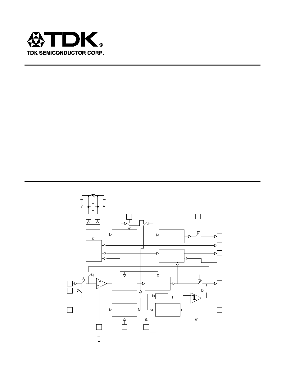
BLOCK DIAGRAM
OSC1
OSC2
OSC
13
14
TXD
12
7(67
TEST
7;
7
16
15
PHASE
COHERENT
WAVE
SYNTHESIZER
PROGRAMMABLE
DIGITAL
DIVIDER
DIGITAL
TIMING
SIGNALS
SYNC
PHASE LOCKED
LOOP
TXA
CLK
9
15
SYNC
6<1
7(67
TEST
SLICER
RXA
FIL
5
2
DIGITAL
DEMODULATOR
DIGITAL
LP
FILTER
DELAY
TEST
7(67
11
RXD
TEST
6
RANDOM
SEQUENCE
GENERATOR
SWITCHED CAP
BANDPASS
FILTER
4
RXF
3
CAP
1
VDD
8
VSS

73M223
1200 Baud FSK Modem
2
FUNCTIONAL DESCRIPTION
The 73M223 has four main functional sections:
timing, transmit, receive, and test. Each section of
the chip will be individually described below.
TIMING
The timing section contains the oscillator (OSC) and
logic which generates digital timing signals used
throughout the chip. The time base can be derived
from 3.18 MHz crystal or an external digital input.
The digital timing logic divides the oscillator
frequency to give a 1200 Hz output than can be
used for system timing. The signaling frequencies
are 1302 Hz for logic "1" and 2097 Hz for logic "0."
The modem will operate with clock inputs from 330
kHz to 7.0 MHz. However, the signaling frequencies
and the system timing will be directly proportional to
the difference in clock frequency.
TRANSMITTER
The 73M223 transmitter consists of a programmable
divider that drives a coherent phase frequency
synthesizer. The programmable divider is digitally
controlled via the Data Input pin (TXD). The output
of the divider clocks a 16 segment phase coherent
frequency synthesizer. A sine wave is constructed
by eight weighted capacitors which are the inputs to
a low pass filter. The synthesized signal is output
directly to the transmit pin TXA. The transmit signal
can be disabled by using the digital control pin
7;
.
RECEIVER
The 73M223's receiver is comprised of three
sections: the input bandpass filter, the
synchronization loop, and the demodulator.
The input bandpass filter is a four pole Butterworth
filter, implemented using switched capacitor
technology. This filter reduces wideband noise which
significantly improves data error rates. The 73M223
can be configured with the bandpass filter in series
with the receiver by setting FIL = 1 and inserting the
received signal at RXF (recommended
configuration). The bandpass filter can be deleted
from the system by setting FIL = 0 and inputting the
received signal through RXA.
The demodulator is used to detect a received mark
or space.
The synchronization for sampling the digital output at
RXD is derived from a digital phase locked loop. The
phase locked loop is clocked at 16 times the bit rate
with a maximum lock period of 8 clocks to lock on
the data output signal. When
6<1
is low the output
of SYNC is nominally 1200 Hz, but is resynchronized
to the center of the data bit on each data transition.
When
6<1
is high, SYNC will output a 1200 Hz
clock, which is not synchronized to the data on RXD.
SELF TEST MODE
The 73M223 features an autotest mode which
provides easy field test capability of the chip's
functionality. The modem is placed in the test mode
by taking the test pin high. In the test mode the Data
Input pin is disconnected and the programmable
divider is driven by a pseudo random PN sequence
generator and the transmitter's output is connected
to the receiver's input. The input data to the
programmable divider is delayed by the system
delay time and compared to the digital output on
sync transitions. If the detected data matches the
delayed input data from the PN sequence counter,
the 73M223 is properly functioning as indicated by
RXD low. A high on the RXD pin indicates a
functional problem on the 73M223.
73M223
1200 Baud FSK Modem
3
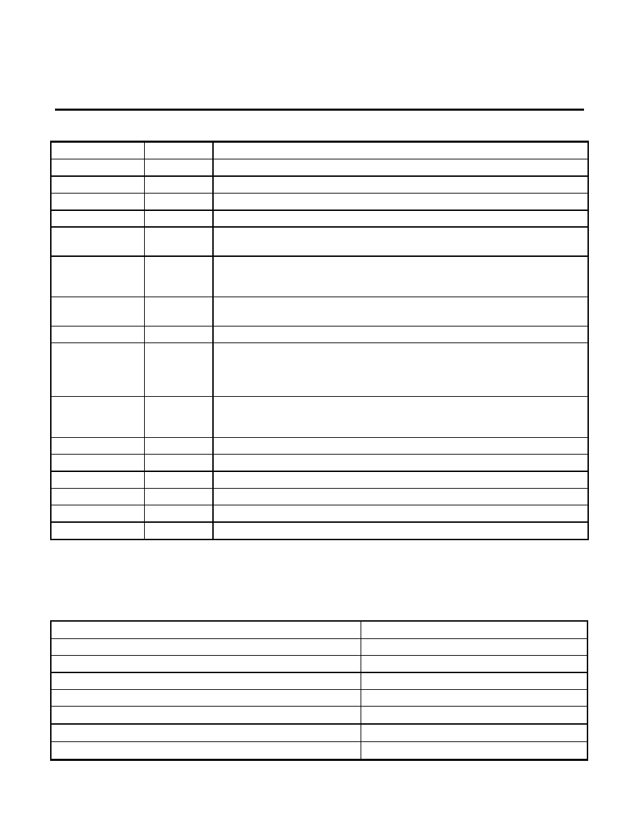
PIN DESCRIPTION
PIN NO.
PIN NAME
DESCRIPTION
1
VDD
Positive Supply Voltage. Bypasses to Vss with 0.1 µF capacitor.
2
RXA
Receive Analog Input. Analog input from the telephone network.
3
CAP
Capacitor. Connect a 0.1µF capacitor between Pin 3 and ground (VSS).
4
RXF
Filtered Receive Analog Input
5
FIL
Analog Input Control. A logical 1 selects the filtered input. A logical 0 selects
the non-filtered input.
6
TEST
Self-Test Mode Control. Normal operation when a logical 0.A logical 1 places
the device into the self-test mode. A low appears at RXD, to indicate a
properly functioning device.
7
7;
Transmitter Control. A logical 0 selects transmit mode. A logical 1 selects a
stand-by condition forcing TXA to VDD/2 VDC.
8
VSS
Ground
9
SYNC
Synchronous Clock Output. Digital output synchronized with the 1200 bit/s
received data when
6<1 LV ORZ
and used to sample the received data or eye
pattern. The falling edge of SYNC should be used to sample RXD. When
6<1
LV KLJK D
1200 H
] FORFN LV RXWSXW
10
6<1
Sync Enable. A logic 0 locks the SYNC clock PLL to the 1200 baud receive
data. A logic 1 disables the receive data PLL, and connects SYNC to the 1200
HZ reference.
11
RXD
Receiver Digital Output
12
TXD
Transmitter Digital Input
13
OSC
1
Crystal Input (3.1872 MHz) or External Clock Input
14
OSC
2
Crystal Return
15
CLK
1200 Hz Square wave Output. Can drive up to 10 CMOS loads.
16
TXA
Transmitter Analog Output
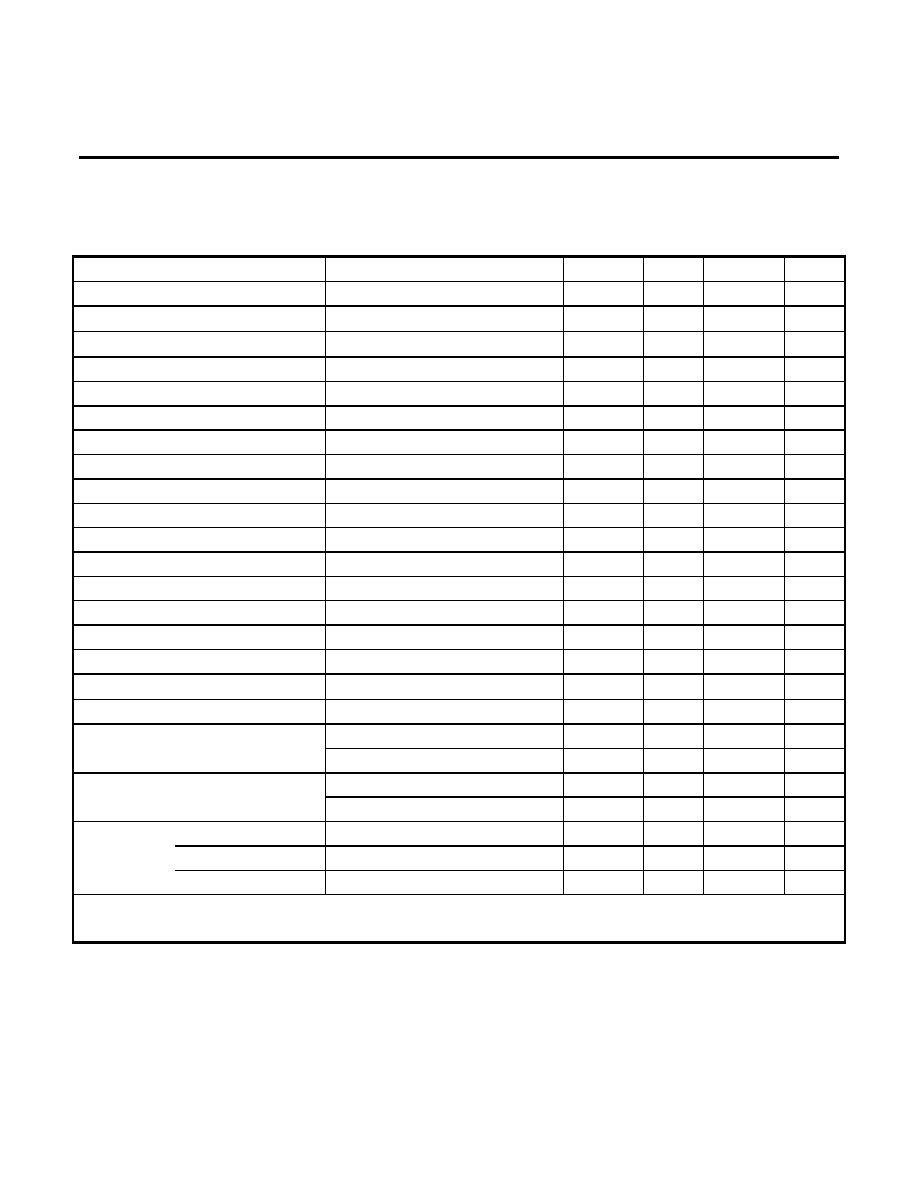
ELECTRICAL SPECIFICATIONS
Recommended conditions apply unless otherwise specified.
ABSOLUTE MAXIMUM RATINGS
Operation outside these rating limits may cause permanent damage to this device.
PARAMETER
RATING
Power Supply Voltage (VDD-VSS)
14 V
Analog Input Voltage at RXA
- 0.3 to VDD V
Analog Input Voltage at RXF
- 3 to VDD V
Digital Input Voltage
VSS ≠ 0.3 to VDD + 0.3 V
Storage Temperature Range
- 65 to + 150
∞
C
Operating Temperature Range
- 25 to + 70
∞
C
Lead Temperature (10 secs soldering)
260
∞
C
73M223
1200 Baud FSK Modem
4
ELECTRICAL CHARACTERSITICS
Unless otherwise specified, 4.5 <VDD <13 VDC, VSS = 0 VDC, -25
∞
C <TA
POWER SUPPLY
PARAMETER
TEST CONDITIONS
MIN
NOM
MAX
UNIT
VDD Voltage Supply Range
4.5
13
V
Supply Current
VDD = 5V 25
∞
C
2.0
mA
VDD = 12V 25
∞
C
5.0
mA
Digital Inputs
Input Low Voltage VIL
VSS - 0.3
VSS + 1.5
V
Input High Voltage VIH
VDD - 1.5
VDD + 0.3
V
Input Low Current IIL
-1
µA
Input High Current IIH
1
µA
Digital Outputs
Output Low Voltage VOL
IOL < 1 µA
0.05
V
Output High Voltage VOH
IOL < -1 µA
VDD = 5V
4.95
V
Output Low Current IOL
VOL = 0.4V
VDD = 5V
0.5
mA
Output High Current IOH
VOH = 4.5V
VDD = 5V
-0.2
mA
Analog Input Level @ RXA
Centered at VDD/2 + 0.5V
0.2
VDD/4
Vpp
Analog Input Level @ RXF
*DC Level between VDD & VSS
0.2
VDD/2
VDC
Error Rate
S/N = 8 dB Input @ RXF
5 x 10
-3
Analog Output Level @ TXA
RL
10K
7;
= 0
VDD/4
Vpp
7;
= 1
VDD/2
VDC
XTAL = 3.1872 MHz
TXD=1
1302
Hz
Output Frequency @ TXA
TXD=0
2097
Hz
2nd to 14th Harmonics
-60
-50
dB
Output Harmonics
15th Harmonic
-20
dB
Input Filter (RFX)
*Input = 200 mVp-p to VDD/2 Vp-p
Lower 3 dB Corner
760
Hz
Upper 3 dB Corner
2625
Hz
* Note: The 73M223 RXF input is AC coupled internally but the DC value of the input must be between the two
supplies VDD & VSS.
73M223
1200 Baud FSK Modem
5
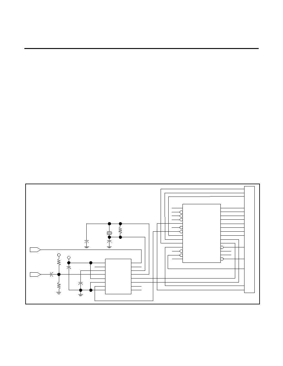
APPLICATION INFORMATION
The 73M223 modem chip allows low cost
communications in a private network, utilizing
twisted pair telephone wires. This chip is the prime
choice of those designers who require an efficient,
high performance modem solution for dedicated
private networks, HDX dial-up and other specialized
applications. Such applications include credit
verification systems, point-of-sale terminals, remote
process control, satellite and RF telemetery, private
data links and acoustic modem designs. No
microprocessors or external adjustments are
necessary with this device.
Utilizing a crystal input of 3.1872 MHz*, the 73M223
is a V.23 main channel 1200 Baud, FSK modem.
The signaling frequencies generated are 1302 Hz for
a logic "1" and 2097 Hz for a logic "0." Crystals with
frequencies varying between 330 kHz to 7.0 MHz or
higher can be used. The baud rate and signaling
frequencies vary linearly with variation in crystal
frequency. If compatibility with V.23 is not required, a
color burst 3.579 MHz crystal can be used as long
as the other modem uses the same frequency offset.
A typical implementation on the 73M223 is shown in
the figure below. A 73M1550 UART receives data to
be transmitted from a microprocessor bus. The
UART sends the data in a serial format to the
73M223 modem after inserting the necessary start
and stop bits. The modem transmits this data to the
far end via the TXA pin. Full-duplex operation can be
implemented by utilizing separate transmit and
receive circuits. A USART can be used instead of a
UART if synchronous operation is desired. With
synchronous operation, a USART uses the modem's
SYNC signal for timing to sample the received data,
and the modem's CLK signal for timing to send data
to be transmitted.
* Available from Ecliptek Corp. (714) 433-1200 and
SMI Inc. (916) 477-5085.
73M223 TYPICAL APPLICATION
RXA
TXA
R2
100K
C5
VDD
0.1 µF
R3
100K
0.1 µF
C3
1 µF
C4
VDD
C2
30 pF
Typ.
3.1872
MHz
Y1
R1
1 M
C1
30 pF
Typ.
U1
1
2
3
4
5
6
7
8
VDD
RXA
CAP
RXF
TXA
CLK
OSC2
OSC1
TXD
FIL
TEST
RXD
7;
VSS
6<1
SYNC
73M223
9
10
11
12
13
14
15
16
U1
28
27
26
25
24
23
22
21
20
19
18
17
16
15
14
13
12
11
10
9
8
7
6
5
4
3
2
1
VCC
'&'
'65
&76
MR
'75
576
A0
A1
A2
INTRPT
5,
5'
VSS
:5
XOUT
XIN
&6#
SOUT
SIN
D7
D6
D5
D4
D3
D2
D1
D0
H
O
S
T
I
N
T
E
R
F
A
C
E
16C550