
78P2252
STM-1/OC-3
Transceiver
JUNE 2002
DESCRIPTION
The 78P2252 is a transceiver IC designed for
155.52Mbit/s (OC-3 or STM-1) transmission. It is
used at the interface to a fiber optic module.
Interface to digital framer circuits is accomplished via
a serial PECL or parallel CMOS interface.
The 78P2252 is built in a BiCMOS technology
allowing for high performance with low power
operation. The device automatically adjusts for
operations with either a 3.3V or 5V power supply
and is packaged in a 64-pin TQFP.
FEATURES
∑ Compliant with ITU-T G.958 jitter tolerance,
Telcordia TR-NWT-00253, ANSI T1.105.03-
1994, and ANSI T1.105.05-1994
∑ Integrated Clock Recovery Unit (CRU)
∑ Serial PECL Interface
∑ Four and Eight bit Parallel CMOS Interfaces
∑ PECL Interfaces for connection to Fiber
Optic Modules for SONET OC3 applications
∑ Integrated Clock Multiplier PLL
∑ Advanced BiCMOS Process
∑ Available in 64TQFP Package
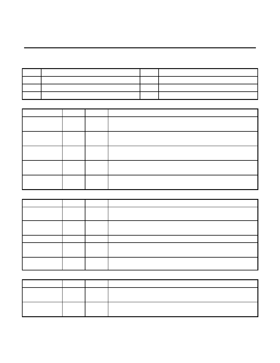
BLOCK DIAGRAM
Crystal
Oscillator
Clock
Generator
Clock
Recovery
Bias
X
T
A
L
2
X
T
A
L
1
R
F
O
ECLINN
ECLINP
ECLOUTN
ECLOUTP
CKIN
TXCK
TXCKP,N
TXDTP,N
RXDTP,N
RXCKP,N
L
L
B
A
C
K
RLBACK
L
F
TXDT[7:0]
RXDT[7:0]
RXCK
8
B
I
T
/
$
B
I
T
P
A
R
/S
E
R
H
U
B
/
H
O
S
T

78P2252
STM-1/OC-3
Transceiver
2
FUNCTIONAL DESCRIPTION
The 78P2252 contains all the necessary transmit
and receive circuitry for connection between
155.52Mbit/s signals and digital Framer/Deframer
ICs.
DIGITAL INTERFACE
The digital interface of the 78P2252 can operate as
a Serial PECL, 4-bit Parallel CMOS, or 8-bit Parallel
CMOS interface. These modes are controlled by the
PAR/
SER and 8BIT/$BIT pins as shown in the
following table.
Mode
PAR/
SER
SER
SER
SER
8BIT/
$BIT
$BIT
$BIT
$BIT
Data pins Clock pins
Clock Frequency
(MHz)
Serial 0 X
TXDTP,N
RXDTP,N
TXCKP,N
RXCKP,N
155.52
4-bit
Parallel
1 0
TXDT[3:0]
RXDT[3:0]
TXCK
RXCK
38.88
8-bit
Parallel
1 1
TXDT[7:0]
RXDT[7:0]
TXCK
RXCK
19.44
TRANSMITTER OPERATION
The transmitter accepts serial or parallel data and
generates an NRZ coded PECL signal for
transmission to a fiber optic module.
When set to serial mode via PAR/
SER pin, serial
data is input from the digital Framer/Deframer IC to
the 78P2252 on the TXDTP and TXDTN pins at
PECL levels. The data is clocked in with a line rate
frequency clock generated by the 78P2252 on the
TXCKP and TXCKN pins.
When set to parallel mode, parallel data is input from
the digital Framer/Deframer IC to the 78P2252 on
the TXDT[7:0] pins. Eight bits or four bits of data are
used depending the setting of the 8BIT/
$BIT pin.
o
In eight bit parallel mode, data is read on
pins TXDT[7:0].
o
In four bit parallel mode, data is read on pins
TXDT[3:0].
The parallel input data is clocked in with the
generated clock output TXCK. The
TXCK
automatically adjusts to either one-eighth or one-
fourth the standard line rate frequency, depending
on the state of the 8BIT/
$BIT pin.
RECEIVER OPERATION
The receiver accepts NRZ coded, serial data at
155.52Mbit/ from the fiber optic module via the ECL
inputs, ECLINP and ECLINN. A clock signal is
recovered using a low jitter PLL circuit.
In serial mode, the received data is output on the
RXDTP and RXDTN pins and the recovered clock is
output on the RXCKP and RXCKN pins at the line
rate frequency.
In parallel mode, the received data is converted to
either eight bit or four bit parallel formats,
determined by the state of the 8BIT/
$BIT pin. The
first bit received will arrive on the most significant
output pin, RXDT[7] in eight bit mode and RXDT[3]
in four bit mode. In parallel mode, the recovered
clock in output on the RXCK pin at either one-eighth
or one-fourth the line rate frequency, depending on
the state of the 8BIT/
$BIT pin.

78P2252
STM-1/OC-3
Transceiver
3
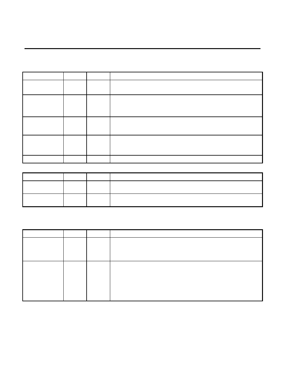
LOOPBACK OPERATION
Remote and Local Loopback modes in the 78P2252
are controlled by the RLBACK and LLBACK pins
respectively.
When in Remote (Digital) Loopback mode
(RLBACK logic high), the received data is internally
routed onto the transmitter inputs. Note that any
input data on the TXDTP,N pins or TXDT[7:0] pins is
ignored in remote loopback mode.
Crystal
Oscillator
Clock
Generator
Clock
Recovery
Bias
X
T
A
L
2
X
T
A
L
1
R
F
O
ECLINN
ECLINP
ECLOUTN
ECLOUTP
CKIN
TXCK
TXCKP,N
TXDTP,N
RXDTP,N
RXCKP,N
L
L
B
A
C
K
RLBACK
L
F
TXDT[7:0]
RXDT[7:0]
RXCK
8
B
I
T
/
$
B
I
T
P
A
R
/S
E
R
H
U
B
/
H
O
S
T
Remote (Digital)
Loopback
When in Local (Analog) Loopback mode
(LLBACK logic high), the transmit output signals are
internally routed to the receiver inputs. Note that
Local Loopback mode is disabled when HUB/
HOST
is low or RLBACK is high.
Crystal
Oscillator
Clock
Generator
Clock
Recovery
Bias
X
T
A
L
2
X
T
A
L
1
R
F
O
ECLINN
ECLINP
ECLOUTN
ECLOUTP
CKIN
TXCK
TXCKP,N
TXDTP,N
RXDTP,N
RXCKP,N
L
L
B
A
C
K
RLBACK
L
F
TXDT[7:0]
RXDT[7:0]
RXCK
8
B
I
T
/
$
B
I
T
P
A
R
/S
E
R
H
U
B
/
H
O
S
T
Local (Analog)
Loopback
REFERENCE CLOCK
The HUB/
HOST pin selects the source of the
reference signal used for the internal transmit clock
generator.
In Hub mode (HUB/
HOST logic high), the transmit
clock reference is derived from either a crystal
oscillator applied to the XTAL1 and XTAL2 pins or a
reference clock input applied at the CKIN pin. The
reference frequency should be one-eighth the line
rate frequency at 19.44MHz and should be applied
in one of the following configurations.
XTAL1
XTAL2
CKIN
XTAL1
XTAL2
CKIN
Hub Mode Configurations
Using crystal -- or -- Using external clock
In Host mode (HUB/
HOST logic low), the transmit
clock reference is derived from the recovered receive
clock. Note that the recovered receive clock is also
used as the reference clock when Remote Loopback
is enabled.
LLBACK RLBACK HUB/
HOST
HOST
HOST
HOST Reference Clock
0 0 1
CKIN or
XTAL1,2
1 0 1
CKIN or
XTAL1,2
X 1 1
Recovered Rx
Clock
X X 0
Recovered Rx
Clock
78P2252
STM-1/OC-3
Transceiver
4
PIN DESCRIPTION
LEGEND
TYPE DESCRIPTION
TYPE DESCRIPTION
A
Analog Pin
PI
PECL Digital Input
CI
CMOS Digital Input
PO
PECL Digital Output
CO
CMOS Digital Output
S
Supply Pin
TRANSMIT PINS
NAME PIN
TYPE
DESCRIPTION
TXDTP
TXDTN
19
20
PI
Transmit Data Inputs - Serial Mode.
TXCKP
TXCKN
22
23
PO
Transmit Clock Output - Serial Mode.
TXDT[7:0] 11-18
CI
Transmit Data Inputs ≠ Parallel Mode.
TXDT[7:4] are ignored in 4 bit mode.
TXCK 10
CO
Reference Clock Output ≠ Serial mode.
Transmit Clock Output ≠ Parallel Mode.
ECLOUTP
ECLOUTN
56
55
PO Transmit
Outputs.
RECEIVE PINS
NAME PIN
TYPE
DESCRIPTION
ECLINP
ECLINN
52
51
PI
Receiver inputs.
RXCKP
RXCKN
25
26
PO
Recovered Receive Clock ≠ Serial Mode.
RXCK
38
CO
Recovered Receive Clock ≠ Parallel Mode.
RXDTP
RXDTN
27
28
PO
Receive data ≠ Serial Mode.
RXDT[7:0] 30-37
CO
Receive data ≠ Parallel Mode. In 4 bit mode RXDT[3:0] are used and
RXDT[7:4] are pulled low.
REFERENCE CLOCK PINS
NAME PIN
TYPE
DESCRIPTION
XTAL1
XTAL2
5
6
A
Crystal Pins.
These pins should be left floating if using reference clock input CKIN.
CKIN 9
CI
Reference clock input.
This pin should be grounded if using the crystal oscillator inputs.
78P2252
STM-1/OC-3
Transceiver
5
PIN DESCRIPTION
(continued)
CONTROL AND STATUS PINS
NAME PIN
TYPE
DESCRIPTION
RLBACK 41
CI
Remote (Digital) Loopback Enable.
When logic high, loops receiver output data to transmitter inputs.
LLBACK 42
CI
Local (Analog) Loopback Enable.
When logic high, loops transmitter output to receiver input.
Note: Disabled when HUB/
HOST is low or RLBACK is high.
HUB/
HOST
2 CI
In HUB mode (input high) the transmit reference clock is derived from
the CKIN pin or the crystal oscillator. In HOST mode (input low) the
transmit reference clock is derived from the recovered receive clock.
8BIT/
$BIT 63
CI
When in parallel mode, logic high selects 8-bit mode and logic low
selects 4-bit mode.
Ignored in serial mode.
PAR/
SER
62
CI
Selects parallel mode when high, serial mode when low.
ANALOG PINS
NAME PIN
TYPE
DESCRIPTION
RFO 46
A
External reference resistor. See APPLICATION INFORMATION
section for more info.
LF 44
A
PLL loop filter capacitor. See APPLICATION INFORMATION section
for more info.
POWER SUPPLY PINS
It is recommended that all VCC pins be connected to a single power supply plane and all GND pins be connected
to a single ground plane.
NAME PIN
TYPE
DESCRIPTION
VCC
3, 8, 24,
40, 43,
53, 54,
57
S Power
Supply.
GND
1, 4, 7,
21, 29,
39, 45,
47, 48,
50, 58,
59, 60,
61, 64
S Ground.