
Advanced Information
78P2253
E4/STM-1/STS-3/OC-3
Transceiver
November 2000
DESCRIPTION
The 78P2253 is a transceiver IC designed for
139.264Mbit/s (E4) or 155.52Mbit/s (OC-3, STS-3 or
STM-1) transmission. It is used at the interface to a
75
coaxial cable using CMI coding or a fiber optic
module. Interface to digital framer circuits is
accomplished via a serial PECL or parallel CMOS
interface.
The transmitter includes a PLL to multiply the
reference clock to the transmission frequency. The
receiver provides adaptive equalization for accurate
clock and data recovery. The 78P2253 is built in a
BiCMOS technology for high performance and low
power operation. It operates with a 3.3V or 5V power
supply and is packaged in a 64-pin TQFP.
FEATURES
∑
139.264Mbit/s or 155.52Mbit/s interface for
CMI coded transmission using 75
coaxial
cable
∑
Compliant with ITU-T G.703, G.823 jitter
tolerance, Telcordia TR-NWT-00253
∑
Integrated Clock Recovery Unit (CRU)
∑
Serial PECL Interface
∑
Four and Eight bit Parallel CMOS Interfaces
∑
PECL Interfaces for connection to Fiber
Optic Modules for SONET OC3 applications
∑
Adaptive Equalization
∑
Integrated Clock Multiplier PLL
∑
Advanced BiCMOS Process
BLOCK DIAGRAM
Crystal
Oscillator
Clock
Generator
Binary
to CMI
Clock
Recovery
Adaptive
Equalizer
CMI to
Binary
Bias
XT
AL
2
XT
AL
1
CM
I/
ECL
RF
O
LOS
ECLINN
ECLINP
CMIINN
CMIINP
ECLOUTN
ECLOUTP
CMIOUTN
CMIOUTP
CKIN
TXCK
TXCKP,N
TXDTP,N
RXDTP,N
RXCKP,N
LL
BACK
RLBACK
LF
Signal
Detector
TXDT[7:0]
RXDT[7:0]
RXCK
8B
IT/
$BIT
E4
/
SONET
PAR/
SER
HUB/
HOST

78P2253
E4/STM-1/STS-3/OC-3
Transceiver
2
FUNCTIONAL DESCRIPTION
The 78P2253 contains all the necessary transmit
and receive circuitry for connection between
139.264Mbit/s or 155.52Mbit/s signals and digital
Framer/Deframer ICs.
Operating Rate
The 78P2253 has a variety of operating modes and
rates. They are summarized in the tables below.
More detailed descriptions can be found in the
sections that follow.
Standard
E4/SONET
CMI/ECL
Rate
(Mbit/s)
Reference
Frequency
(MHz)
Active I/O
OC-3
STM1 optic
0
0
155.52
19.44
ECL
STS-3
STM-1 Coax
0
1
155.52
19.44
CMI
1
0
139.264
17.408
ECL
E4
1
1
139.264
17.408
CMI
The digital interface of the 78P2253 can be either
Serial PECL, 4-bit Parallel CMOS or 8-bit Parallel
CMOS.
Mode
PAR/SER
8BIT/BIT
Data pins
Clock
pins
Clock
Frequency
(MHz)
Serial
0
X
TXDTP,N
RXDTP,N
TXCKP,N
RXCKP,N
155.52(Sonet)
139.264 (E4)
4-bit
Parallel
1
0
TXDT[3:0]
RXDT[3:0]
TXCK
RXCK
38.88(Sonet)
34.816(E4)
8-bit
Parallel
1
1
TXDT[7:0]
RXDT[7:0]
TXCK
RXCK
19.44(Sonet)
17.408(E4)
Transmit timing is derived from either the reference
clock (the crystal oscillator or CKIN), or the
recovered receive clock. LLBACK and RLBACK
control the local and remote loopback modes
respectively.
LLBACK
RLBACK
HUB/HOST
Transmit Clock derived from
0
0
1
Reference
1
0
1
Reference
X
1
1
Receiver
X
X
0
Receiver
Medium Choices
The CMI/
ECL
pin selects one of two media for
transmission.
When the CMI/
ECL
pin is high, the chip is in CMI
mode and a 75
coaxial cable is used as the
transmission medium. In this mode, the CMIOUTP
and CMIOUTN pins are active. They connect the
chip to the coaxial cable through a transformer and
matching resistors. In CMI mode the transmitter
shapes the transmit pulses to meet the appropriate
template and the adaptive equalizer corrects the
received signal for dispersive attenuation. The
ECLOUTP and ECLOUTN pins are inoperative and
should be left open.
When the CMI/
ECL
pin is low the chip is in ECL
mode and a fiber optics transceiver is used. The
output data signal from the pins ECLOUTP and
ECLOUTN have PECL levels. In this mode, the CMI
pins are inoperative and should be left open. The
CMI encoder and decoder are disabled.
TRANSMITTER OPERATION
The transmitter section generates an analog signal
for transmission through a transformer onto the
coaxial cable or fiber optic module.
When the PAR/
SER
pin is low the chip is in serial
mode. Serial data is input to the 78P2253 on the
TXDTP and TXDTN pins at PECL levels. The data is
timed with the clock generated by the 78P2253 on
the TXCKP and TXCKN pins. In this mode the
8BIT/
$BIT
pin is ignored.
When the PAR/SER pin is high the chip is in parallel
mode. Parallel data is in put to the 78P2253 on the
TXDT[7:0] pins. The input data is timed with the
clock output from TXCK. When 8BIT/
$BIT
is high all
eight bits of TXDT[7:0] are used and the clock
frequency at TXCK is one-eighth the standard
frequency. When 8BIT/
$BIT
is low the lower four
bits, TXCK[3:0] are used and TXCK is one-fourth the
standard frequency.
The first bit output from the ECL/CMI interface is the
most significant bit on the parallel interface, TXDT7
in eight bit mode, TXDT3 in four bit mode.
The clock is generated by a phase-locked oscillator
(PLO). The PLO is locked to a crystal oscillator
operating at one-eighth of the standard clock
frequency, 19.44MHz for OC-3, STS-3 and STM-1
and 17.408MHz for E4. This is shown in Figure 1a.
An external clock signal at CKIN may also be
substituted for a crystal as the reference frequency
for the chip. In this mode, XTL1 and XTL2 must be
configured as shown in Figure 1b. Note that the chip
can be in either ECL or CMI mode when using either
an external clock or a crystal for the reference. In
serial mode the reference clock is output from
TXCK. In parallel mode, the parallel transmit clock is
output from TXCK.

78P2253
E4/STM-1/STS-3/OC-3
Transceiver
3
TRANSMITTER OPERATION (continued)
XTAL1
XTAL2
CKIN
FIGURE 1A: USING CRYSTAL
XTAL1
XTAL2
CKIN
17.283 MHz (E4)
19.440 MHz (Sonet)
FIGURE 1B: USING EXTERNAL CLOCK
In ECL mode the data signal is converted to CMI
code by the Binary to CMI encoded.
The HUB/
HOST
input changes the reference signal
for the clock generator. In the hub mode (HUB/
HOST
high), the transmit clock reference is derived from
either the crystal oscillator or CKIN. In host mode
(HUB/
HOST
low), the transmit clock reference is
derived from the recovered receive clock.
RECEIVER OPERATION
The receiver accepts serial, CMI coded data, at
155.52Mbit/s or 139.264Mbit/s from either the CMI
or the ECL inputs. In CMI mode, the inputs CMIINP
and CMIINN receive the input signal from a coaxial
cable that is transformer-coupled to the chip. The
ECL pins should be left open. In ECL mode, the pins
ECLINP and ECLINN receive the input signal.
In CMI mode, the received signal is equalized for
dispersive cable attenuation and decoded in the CMI
to binary decoder.
A clock signal is recovered using a low jitter PLL
circuit.
The data is converted to binary by the CMI to Binary
decoder.
In serial mode, the received data is output on the
RXDTP and RXDTN pins and the recovered clock is
output on the RXCKP and RXCKN pins.
In parallel mode, the received data is converted to
parallel, eight bits if 8BIT/
$BIT
is high and four if it is
low. The first bit received will arrive on the most
significant output pin, RXDT[7] in eight bit mode and
RXDT3 in four bit mode.
The LOS pin goes high when the signal detector
detects a loss-of-signal condition.
LOOPBACK OPERATION
The 78P2253 is capable of performing signal
loopback in two ways The RLBACK pin selects the
remote loopback mode. In this mode, the received
signal is "looped back" and sent out of transmitter in
place of the transmit input signal.
The LLBACK pin selects the local loop-back mode,
and causes the receiver to use the transmitter output
signal as its input. Local loopback is disabled when
HUB/
HOST
is low or RLBACK is high.

78P2253
E4/STM-1/STS-3/OC-3
Transceiver
4
PIN DESCRIPTION
LEGEND
TYPE
DESCRIPTION
TYPE
DESCRIPTION
A
Analog Pin
PI
PECL Digital Input
CI
CMOS Digital Input
PO
PECL Digital Output
CO
CMOS Digital Output
S
Supply Pin
TRANSMIT PINS
NAME
PIN
TYPE
DESCRIPTION
TXDTP
TXDTN
19
20
PI
Transmit Data Inputs - Serial Mode.
TXCKP
TXCKN
22
23
PO
Transmit Clock Output - Serial Mode.
TXDT[7:0]
11-18
CI
Transmit Data Inputs ≠ Parallel Mode. TXDT[7:4] are ignored in 4 bit
mode.
TXCK
10
CO
Reference Clock Output ≠ Serial mode.
Transmit Clock Output ≠ Parallel Mode.
CMIOUTP
CMIOUTN
60
59
A
Transmit Output in CMI mode.
No signal is output in ECL mode.
ECLOUTP
ECLOUTN
56
55
PO
Transmit Outputs for ECL mode.
No signal is output in CMI mode.
RECEIVE PINS
NAME
PIN
TYPE
DESCRIPTION
CMIINP
CMIINN
50
49
A
Receive inputs in CMI mode.
Transformer coupled from the coaxial cable.
Ignored in ECL mode.
ECLINP
ECLINN
52
51
PI
Receiver inputs in ECL mode.
Ignored in CMI mode.
RXCKP
RXCKN
25
26
PO
Recovered Receive Clock ≠ Serial Mode.
RXCK
38
CO
Recovered Receive Clock ≠ Parallel Mode.
RXDTP
RXDTN
27
28
PO
Receive data ≠ Serial Mode.
RXDT[7:0]
30-37
CO
Receive data ≠ Parallel Mode. In 4 bit mode RXDT[3:0] are used and
RXDT[7:4] are pulled low.

78P2253
E4/STM-1/STS-3/OC-3
Transceiver
5
PIN DESCRIPTION
(continued)
REFERENCE CLOCK PINS
NAME
PIN
TYPE
DESCRIPTION
XTAL1
XTAL2
5
6
A
Crystal Pins. Connect as in Figure 1a.
CKIN
9
CI
Reference clock input. The crystal oscillator connections should be
left open.
CONTROL AND STATUS PINS
NAME
PIN
TYPE
DESCRIPTION
RLBACK
41
CI
Loopback receiver output to transmitter input.
LLBACK
42
CI
Loopback transmitter output to receiver input. Disabled when
HUB/
HOST
is low or RLBACK is high.
HUB/
HOST
2
CI
In HUB mode (input high) the transmit reference clock is derived from
the CKIN pin or the crystal oscillator. In HOST mode (input low) the
transmit reference clock is derived from the recovered receive clock.
CMI/
ECL
1
CI
Selects CMI (input high) or ECL (input low) modes.
E4/
SONET
64
CI
When high, E4 (139.264 Mbit/s) operation is selected. When low,
STM-1/STS-3/OC-3 (155.52Mbit/s) operation is selected.
8BIT/
$BIT
CI
Selects 8 bit parallel data when high and 4 bit parallel mode when
low. In serial mode this pin is ignored.
LOS
39
CO
High during a loss-of-signal condition.
ANALOG PINS
NAME
PIN
TYPE
DESCRIPTION
RFO
46
A
External reference resistor.
LF
44
A
PLL loop filter capacitor.
POWER SUPPLY PINS
It is recommended that all VCC pins be connected to a single power supply plane and all GND pins be connected
to a single ground plane.
NAME
PIN
TYPE
DESCRIPTION
VCC
43
S
Power Supply.
GND
4, 7, 21,
29, 45,
47, 48,
58, 61
S
Ground.

78P2253
E4/STM-1/STS-3/OC-3
Transceiver
6
ELECTRICAL SPECIFICATIONS
ABSOLUTE MAXIMUM RATINGS
Operation beyond these limits may permanently damage the device.
PARAMETER
RATING
Supply Voltage
7 VDC
Storage Temperature
-65 to 150∞ C
Pin Voltage
-0.3 to (V
CC
+0.3) VDC
Pin Current
±
100 mA
RECOMMENDED OPERATING CONDITIONS
Unless otherwise noted all specifications are valid over these temperatures and supply voltage ranges.
PARAMETER
RATING
DC Voltage Supply, VCC
3.3
±
0.3 VDC; 5
±
0.5 VDC
Ambient Operating Temperature
-40 to 85∞C
DC CHARACTERISTICS:
PARAMETER
SYMBOL
CONDITIONS
MIN
NOM
MAX
UNIT
Supply Current (Parallel Mode)
Icc
Vcc = 3.3V
Vcc = 5.0V
140
150
165
175
mA
Supply Current (Serial Mode)
Icc
VCC = 3.3V
VCC = 5.0V
210
280
245
330
mA
DIGITAL INPUT CHARACTERISTICS
Pins of type CI
PARAMETER
SYMBOL
CONDITIONS
MIN
NOM
MAX
UNIT
Input Voltage Low
Vil
0.8
V
Input Voltage High
Vih
2.0
V
Input Current
Iil, Iih
-10
10
µ
A
Input Capacitance
Cin
10
pF
Pins of type PI
PARAMETER
SYMBOL
CONDITIONS
MIN
NOM
MAX
UNIT
Input Voltage Low
Vil
Relative to Vcc
-1.5
V
Input Voltage High
Vih
Relative to Vcc
-1.1
V

78P2253
E4/STM-1/STS-3/OC-3
Transceiver
7
ELECTRICAL SPECIFICATIONS
(continued)
DIGITAL OUTPUT CHARACTERISTICS
Pins of type CO
PARAMETER
SYMBOL
CONDITIONS
MIN
NOM
MAX
UNIT
Output Voltage Low
Vol
Iol = 2mA
0.6
V
Output Voltage High
Voh
Ioh = -2mA
Vcc ≠
0.6
V
Transition Time
Tt
3.5
ns
Pins of type PO
PARAMETER
SYMBOL
CONDITIONS
MIN
NOM
MAX
UNIT
Output Voltage Low
Vol
Relative to Vcc
-1.8
-1.6
V
Output Voltage High
Voh
Relative to Vcc
-1.1
-0.8
V
Rise Time
Tr
1
ns
Fall Time
Tf
1
ns
DIGITAL TIMING CHARACTERISTICS:
Reference Clock Interface
PARAMETER
SYMBOL
CONDITIONS
MIN
NOM
MAX
UNIT
CKIN to TXCK Propagation
Delay
T
CK
20
ns
CKIN
TXCK
T
CK
78P2253
E4/STM-1/STS-3/OC-3
Transceiver
8
ELECTRICAL SPECIFICATIONS
(continued)
DIGITAL TIMING CHARACTERISTICS
Transmit Interface
PARAMETER
SYMBOL
CONDITIONS
MIN
NOM
MAX
UNIT
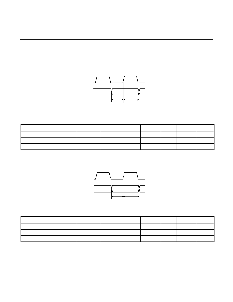
Transmit Setup Time
T
SUs
Serial Mode
1.0
ns
Transmit Hold Time
T
Hs
Serial Mode
-0.5
ns
TXCKP,N Duty Cycle
40
60
%
PARAMETER
SYMBOL
CONDITIONS
MIN
NOM
MAX
UNIT
Transmit Setup Time
T
SUp
Parallel Mode
2.5
ns
Transmit Hold Time
T
Hp
Parallel Mode
0.1
ns
TXCK Duty Cycle
40
60
%
TXCKP -
TXCKN
TXDTP -
TXDTN
T
SUs
T
Hs
TXCK
TXDT[7:0]
T
SUp
T
Hp

78P2253
E4/STM-1/STS-3/OC-3
Transceiver
9
ELECTRICAL SPECIFICATIONS
(continued)
DIGITAL TIMING CHARACTERISTICS
Receive Interface
PARAMETER
SYMBOL
CONDITIONS
MIN
NOM
MAX
UNIT
Receive Propagation Delay
T
PROPs
Serial Mode
1.0
ns
RXCKP,N Duty Cycle
40
60
%
PARAMETER
SYMBOL
CONDITIONS
MIN
NOM
MAX
UNIT
Receive Propagation Delay
T
PROPs
Serial Mode
4.0
ns
RXCKP,N Duty Cycle
40
60
%
RXCKP -
RXCKN
RXDTP -
RXDTN
T
PROPs
RXCK
RXDT[7:0]
T
PROPp

78P2253
E4/STM-1/STS-3/OC-3
Transceiver
10
ELECTRICAL SPECIFICATIONS
(continued)
TRANSMITTER OUTPUT JITTER
The transmit jitter specification ensures compliance with ITU-T G.823 and G.825 and ANSI T1.105.03-1994 for
all supported rates. The corner frequency of the transmit PLL is nominally 3.0 MHz.
PARAMETER
CONDITION
MIN
NOM
MAX
UNIT
Transmitter Output Jitter
200 Hz to 3.5 MHz
0.075
UI
TRANSMITTER SPECIFICATIONS FOR CMI INTERFACE IN E4 MODE
Bit Rate: 139.264Mbit/s
±
15ppm
Code: coded mark inversion (CMI)
The following specifications are met with the external components for E4 operation, above, and configured with
a recommended 1:1 transformer as in Figure 10. With the coaxial output port driving a 75
load, the output
pulses conform to the templates in Figure 4 and Figure 5.
PARAMETER
CONDITION
MIN
NOM
MAX
UNIT
Peak-to-peak Output Voltage
Template
0.9
1.1
V
Rise/ Fall Time
10-90%
2
ns
Negative Transitions
-0.1
0.1
ns
Positive Transitions at Interval
Boundaries
-0.5
0.5
ns
Transition Timing Tolerance
Positive Transitions at mid-
interval
-0.35
0.35
ns
TRANSMISSION PERFORMANCE
PARAMETER
CONDITION
MIN
NOM
MAX
UNIT
Return Loss
7MHz to 240MHz
15
dB
Transmitter
Output
Jitter
Detector
Measured Jitter
Amplitude
200 Hz
3.5 MHz
20dB/decade

78P2253
E4/STM-1/STS-3/OC-3
Transceiver
11
ELECTRICAL SPECIFICATIONS
(continued)
Note 1 ≠ The maximum "steady state" amplitude should not exceed the 0.55V limit. Overshoots and other transients are permitted to fall
into the shaded area bounded by the amplitude levels 0.55V and 0.6V, provided that they do not exceed the steady state level by more
than 0.05V.
Note 2 ≠ For all measurements using these masks, the signal should be AC coupled, using a capacitor of not less than 0.01
µ
F, to the
input of the oscilloscope used for measurements. The nominal zero level for both masks should be aligned with the oscilloscope trace with
no input signal. With the signal then applied, the vertical position of the trace can be adjusted with the objective of meeting the limits of the
masks. Any such adjustment should be the same for both masks and should not exceed
±
0.05V. This may be checked by removing the
input signal again and verifying that the trace lies with
±
0.05V of the nominal zero level of the masks.
Note 3 ≠ Each pulse in a coded pulse sequence should meet the limits of the relevant mask, irrespective of the state of the preceding or
succeeding pulses, with both pulse masks fixed in the same relation to a common timing reference, i.e. with their nominal start and finish
edges coincident. The masks allow for HF jitter caused by intersymbol interference in the output stage, but not for jitter present in the timing
signal associated with the source of the interface signal. When using an oscilloscope technique to determine pulse compliance with the
mask, it is important that successive traces of the pulses overlay in order to suppress the effects of low frequency jitter. This can be
accomplished by several techniques [e.g. a) triggering the oscilloscope on the measured waveform or b) providing both the oscilloscope
and the pulse output circuits with the same clock signal].
Note 4 ≠ For the purpose of these masks, the rise time and decay time should be measured between ≠0.4V and 0.4V, and should not
exceed 2ns.
FIGURE 4 ≠ MASK OF A PULSE CORRESPONDING TO A BINARY ZERO IN E4 MODE
(Note 1)
(Note 1)
(Note 1)
0.60
0.55
0.50
0.45
0.40
0.05
-0.05
-0.50
-0.55
-0.60
-0.45
-0.40
(Note 1)
0.35ns
Nominal
Zero Level
(Note 2)
T = 7.18ns
0.1ns
0.1ns
1ns
1.795 ns
1.795 ns
1.795 ns
1.795 ns
1ns
1ns
1ns
0.1ns
0.1ns
1ns
1ns
Nominal
Pulse
0.35ns
V

78P2253
E4/STM-1/STS-3/OC-3
Transceiver
12
ELECTRICAL SPECIFICATIONS
(continued)
Note 1 ≠ The maximum "steady state" amplitude should not exceed the 0.55V limit. Overshoots and other transients are permitted to fall into the
shaded area bounded by the amplitude levels 0.55V and 0.6V, provided that they do not exceed the steady state level by more than 0.05V.
Note 2 ≠ For all measurements using these masks, the signal should be AC coupled, using a capacitor of not less than 0.01
µ
F, to the input of the
oscilloscope used for measurements. The nominal zero level for both masks should be aligned with the oscilloscope trace with no input signal. With
the signal then applied, the vertical position of the trace can be adjusted with the objective of meeting the limits of the masks. Any such adjustment
should be the same for both masks and should not exceed
±
0.05V. This may be checked by removing the input signal again and verifying that the
trace lies with
±
0.05V of the nominal zero level of the masks.
Note 3 ≠ Each pulse in a coded pulse sequence should meet the limits of the relevant mask, irrespective of the state of the preceding or
succeeding pulses, with both pulse masks fixed in the same relation to a common timing reference, i.e. with their nominal start and finish edges
coincident. The masks allow for HF jitter caused by intersymbol interference in the output stage, but not for jitter present in the timing signal
associated with the source of the interface signal. When using an oscilloscope technique to determine pulse compliance with the mask, it is
important that successive traces of the pulses overlay in order to suppress the effects of low frequency jitter. This can be accomplished by several
techniques [e.g. a) triggering the oscilloscope on the measured waveform or b) providing both the oscilloscope and the pulse output circuits with the
same clock signal].
Note 4 ≠ For the purpose of these masks, the rise time and decay time should be measured between ≠0.4V and 0.4V, and should not exceed 2ns.
Note 5 ≠The inverse pulse will have the same characteristics, noting that the timing tolerance at the level of the negative and positive transitions are
±
0.1ns and
±
0.5ns respectively.
Figure 5 ≠ Mask of a Pulse corresponding to a binary One in E4 mode.
(Note 1)
(Note 1)
0.60
0.55
0.50
0.45
0.40
0.05
-0.05
-0.50
-0.55
-0.60
-0.45
-0.40
(Note 1)
Nominal
Zero Level
(Note 2)
T = 7.18ns
0.1ns
0.1ns
1ns
1.795 ns
1ns
Nominal
Pulse
V
3.59ns
1.35ns
1.35ns
3.59ns
1.795 ns
1ns
1ns
0.5ns
0.5ns

78P2253
E4/STM-1/STS-3/OC-3
Transceiver
13
ELECTRICAL SPECIFICATIONS
(continued)
TRANSMITTER SPECIFICATIONS FOR CMI INTERFACE IN STS-3 (STM-1) MODE
Bit Rate: 155.52Mbit/s
±
20ppm
Code: coded mark inversion (CMI)
The following specifications are met with the external components for STS-1 operation configured with a
recpmmended 1:1 transformer as in Figure 10. With the coaxial output port driving a 75
load, the output
pulses conform to the templates in Figure 6 and Figure 7.
PARAMETER
CONDITION
MIN
NOM
MAX
UNIT
Peak-to-peak Output Voltage
Template
0.9
1.1
V
Rise/ Fall Time
10-90%
2
ns
Transition Timing Tolerance
Negative Transitions
Positive Transitions at Interval
Boundaries
Positive Transitions at mid-
interval
-0.1
-0.5
-0.35
0.1
0.5
0.35
ns
ns
ns
TRANSMISSION PERFORMANCE
PARAMETER
CONDITION
MIN
NOM
MAX
UNIT
Return Loss
7MHz to 240MHz
15
dB

78P2253
E4/STM-1/STS-3/OC-3
Transceiver
14
ELECTRICAL SPECIFICATIONS
(continued)
Note 1 ≠ The maximum "steady state" amplitude should not exceed the 0.55V limit. Overshoots and other transients are permitted to fall into
the shaded area bounded by the amplitude levels 0.55V and 0.6V, provided that they do not exceed the steady state level by more than
0.05V.
Note 2 ≠ For all measurements using these masks, the signal should be AC coupled, using a capacitor of not less than 0.01
µ
F, to the input
of the oscilloscope used for measurements. The nominal zero level for both masks should be aligned with the oscilloscope trace with no input
signal. With the signal then applied, the vertical position of the trace can be adjusted with the objective of meeting the limits of the masks. Any
such adjustment should be the same for both masks and should not exceed
±
0.05V. This may be checked by removing the input signal again
and verifying that the trace lies with
±
0.05V of the nominal zero level of the masks.
Note 3 ≠ Each pulse in a coded pulse sequence should meet the limits of the relevant mask, irrespective of the state of the preceding or
succeeding pulses, with both pulse masks fixed in the same relation to a common timing reference, i.e. with their nominal start and finish
edges coincident. The masks allow for HF jitter caused by intersymbol interference in the output stage, but not for jitter present in the timing
signal associated with the source of the interface signal. When using an oscilloscope technique to determine pulse compliance with the mask,
it is important that successive traces of the pulses overlay in order to suppress the effects of low frequency jitter. This can be accomplished
by several techniques [e.g. a) triggering the oscilloscope on the measured waveform or b) providing both the oscilloscope and the pulse
output circuits with the same clock signal].
Note 4 ≠ For the purpose of these masks, the rise time and decay time should be measured between ≠0.4V and 0.4V, and should not
exceed 2ns.
Figure 6 ≠ Mask of a Pulse corresponding to a binary Zero in STS-3 mode.
(Note 1)
(Note 1)
(Note 1)
0.60
0.55
0.50
0.45
0.40
0.05
-0.05
-0.50
-0.55
-0.60
-0.45
-0.40
(Note 1)
0.35ns
Nominal
Zero Level
(Note 2)
T = 6.43ns
0.1ns
0.1ns
1ns
1.608ns
1.608ns
1.608ns
1.608ns
1ns
1ns
1ns
0.1ns
0.1ns
1ns
1ns
Nominal
Pulse
0.35ns
V

78P2253
E4/STM-1/STS-3/OC-3
Transceiver
15
Note 1 ≠ The maximum "steady state" amplitude should not exceed the 0.55V limit. Overshoots and other transients are permitted to fall into the
shaded area bounded by the amplitude levels 0.55V and 0.6V, provided that they do not exceed the steady state level by more than 0.05V.
Note 2 ≠ For all measurements using these masks, the signal should be AC coupled, using a capacitor of not less than 0.01
µ
F, to the input of the
oscilloscope used for measurements. The nominal zero level for both masks should be aligned with the oscilloscope trace with no input signal.
With the signal then applied, the vertical position of the trace can be adjusted with the objective of meeting the limits of the masks. Any such
adjustment should be the same for both masks and should not exceed
±
0.05V. This may be checked by removing the input signal again and
verifying that the trace lies with
±
0.05V of the nominal zero level of the masks.
Note 3 ≠ Each pulse in a coded pulse sequence should meet the limits of the relevant mask, irrespective of the state of the preceding or
succeeding pulses, with both pulse masks fixed in the same relation to a common timing reference, i.e. with their nominal start and finish edges
coincident. The masks allow for HF jitter caused by intersymbol interference in the output stage, but not for jitter present in the timing signal
associated with the source of the interface signal. When using an oscilloscope technique to determine pulse compliance with the mask, it is
important that successive traces of the pulses overlay in order to suppress the effects of low frequency jitter. This can be accomplished by several
techniques [e.g. a) triggering the oscilloscope on the measured waveform or b) providing both the oscilloscope and the pulse output circuits with
the same clock signal].
Note 4 ≠ For the purpose of these masks, the rise time and decay time should be measured between ≠0.4V and 0.4V, and should not exceed 2ns.
Note 5 ≠The inverse pulse will have the same characteristics, noting that the timing tolerance at the level of the negative and positive transitions
are
±
0.1ns and
±
0.5ns respectively.
Figure 7 ≠ Mask of a Pulse corresponding to a binary One in STS-3 mode
(Note 1)
(Note 1)
0.60
0.55
0.50
0.45
0.40
0.05
-0.05
-0.50
-0.55
-0.60
-0.45
-0.40
(Note 1)
Nominal
Zero Level
(Note 2)
6.43ns
0.1ns
0.1ns
1ns
1.608ns
1ns
Nominal
Pulse
V
3.215ns
1.2ns
1.2ns
3.215ns
1.608ns
1ns
1ns
0.5ns
0.5ns

78P2253
E4/STM-1/STS-3/OC-3
Transceiver
16
ELECTRICAL SPECIFICATIONS
(continued)
RECEIVER SPECIFICATIONS
The following specifications are met with the external components.
PARAMETER
CONDITION
MIN
NOM
MAX
UNIT
LOS Threshold
0.1
V
RECEPTION PERFORMANCE
Return Loss
7MHz to 240MHz
15
dB
RECEIVER JITTER TOLERANCE
STS-3 and OC-3 jitter tolerance specifications are in ANSI T1.105.05-1994 and Telcordia TR-NWT-000253,
Issue 2, Dec. 1991. STM-1 specifications are in ITU-T G.825. They are identical except that STM-1 specifies
both jitter and wander. The E4 specifications are found in ITU-T G.823. The STM-1 specification is the tightest
and covers the largest frequency range.
PARAMETER
CONDITION
MIN
NOM
MAX
UNIT
Receiver Jitter Tolerance
Note 1: Not tested in production
12
µ
Hz to 178
µ
Hz
1.6mHz to 15.6mHz
125mHz to 19.3 Hz
500Hz to 6.5kHz
65kHz to 3.5MHz
2800
311
39
1.5
0.15
UI
0.01
0.1
1
10
100
1000
10000
1.E-06
1.E-05
1.E-04
1.E-03
1.E-02
1.E-01
1.E+00
1.E+01
1.E+02
1.E+03
1.E+04
1.E+05
1.E+06 1.E+07
STM-1
E4

78P2253
E4/STM-1/STS-3/OC-3
Transceiver
17
ELECTRICAL SPECIFICATIONS
(continued)
RECEIVER JITTER TRANSFER FUNCTION
The receiver clock recovery loop filter characteristics such that the receiver has the following transfer function.
The corner frequency of the PLL is approximately 250 kHz.
PARAMETER
CONDITION
MIN
NOM
MAX
UNIT
Receiver Jitter transfer function
below 250 kHz
0.1
dB
Jitter transfer function roll-off
Note 1: Not tested in production
20
dB per
decade
-10
-9
-8
-7
-6
-5
-4
-3
-2
-1
0
1.00E+03
1.00E+04
1.00E+05
1.00E+06
1.00E+07

78P2253
E4/STM-1/STS-3/OC-3
Transceiver
18
ELECTRICAL SPECIFICATIONS
(continued)
RECEIVER SPECIFICATIONS FOR CMI INTERFACE
The following specifications are met with the external components for E4 operation, above, and configured with
a 1:1 recommended. The input signal is assumed compliant with ITU-T G.703 and attenuated by the dispersive
loss of a cable. The minimum cable loss is 0dB and the maximum is shown in Figure 8.
The "Worst Case" line corresponds to the01 ITU-T G.703 recommendation. The "Typical" line corresponds to a
typical installation referred to in ANSI T1.102-1993. The receiver is tested using the cable model on page n. It is
a lumped element approximation of the "Worst Case" line.
Figure 8: Typical and worst-case Cable attenuation
0
5
10
15
20
25
30
1.00E+05
1.00E+06
1.00E+07
1.00E+08
1.00E+09
Frequency (Hz)
Attenuation (dB)
Worst Case
Typical

78P2253
E4/STM-1/STS-3/OC-3
Transceiver
19
APPLICATION INFORMATION
EXTERNAL COMPONENTS:
COMPONENT
PIN(S)
VALUE
UNITS
TOLERANCE
Reference Resistor
RFO
31.6
k
1%
Filter Capacitor
LF1
150
nF
10%
TRANSFORMER SPECIFICATIONS:
COMPONENT
VALUE
UNITS
TOLERANCE
Turns Ratio
1:1
3%
Suggested Manufacturer: Pulse, MiniCircuits
CRYSTAL SPECIFICATIONS:
E4 Operation
COMPONENT
VALUE
UNITS
TOLERANCE
Center Frequency
17.408
MHz
Load Capacitor ≠ XTAL1 to ground; XTAL2 to ground
27
pF
CRYSTAL SPECIFICATIONS:
OC-3, STM-1, STS-3 Operation
COMPONENT
VALUE
UNITS
TOLERANCE
Center Frequency
19.44
MHz
Load Capacitor ≠ XTAL1 to ground; XTAL2 to ground
27
pF

78P2253
E4/STM-1/STS-3/OC-3
Transceiver
20
APPLICATION INFORMATION
(continued)
FIGURE 9. PECL INTERFACE
PECL INTERFACE COMPONENTS:
COMPONENT
VALUE
UNITS
TOLERANCE
Output Bias Resistor, R
BIAS
V
CC
= 5v
V
CC
= 3.3V
250
140
5%
5%
Termination Resistor, R
TERM
100
5%
When the PECL signals travel one inch or less, lower power operation can be achieved by increasing R
BIAS
and
eliminating R
TERM
.
R
BIAS
R
BIAS
R
TERM

78P2253
E4/STM-1/STS-3/OC-3
Transceiver
21
GND
S1 SW DIP-8
1
2
3
4
5
6
7
8
16
15
14
13
12
11
10
9
C26
27pF
J1
13
25
12
24
11
23
10
22
9
21
8
20
7
19
6
18
5
17
4
16
3
15
2
14
1
VCC
+
C18
4.7uF
R12
510
D2 LED
1
2
Isolated ground under
Transformer output
C19
0.1uF
R12
31.6K
T2
ADT1-1WT
6
1
2
4
3
R2 301 1%
U2
Crystal Osc.
Vcc
GND
ENA
OUT
8
4
1
5
C20
0.01uF
U1
78P2253
50
4
49
7
46
21
24
29
60
59
64
3
45
8
1
2
5
6
9
10
18
17
16
15
14
13
12
11
37
36
35
34
33
32
31
30
38
39
40
41
42
43
44
47 48
53 54 57
58 61
63
62
CMIINP
GND
CMINN
GND
RFO
GND
VCC
GND
CMIOUTP
CMIOUTN
E4/SONET
VCC
GND
VCC
CMI/ECL
HUB/HOST
XTAL1
XTAL2
CKIN
TXCK
TXDT0
TXDT1
TXDT2
TXDT3
TXDT4
TXDT5
TXDT6
TXDT7
RXDT0
RXDT1
RXDT2
RXDT3
RXDT4
RXDT5
RXDT6
RXDT7
RXCK
LOS
VCC
RLBACK
LLBACK
VCC
LF
GND GND
VCC VCC
VCC
GND GND
8BIT/4BIT
PAR/SER
RX1
1
2
J2
TX1
1
2
C9
0.1uF
C1
0.1uF
T1
ADT1-1WT
1
5
2
6
C2
0.1uF
VCC
Can oscillator
or sigle crystal
VCC
VCC
C28
1uF
C3
0.1uF
C27
27pF
R1 75 1%
C8
0.1uF
33
Y1
CRYSTAL
FIGURE 10: RECOMMENDED APPLICATION CIRCUIT, STM-1 COAX SERIAL INTERFACE

78P2253
E4/STM-1/STS-3/OC-3
Transceiver
22
MECHANICAL SPECIFICATIONS
64-TQFP Mechanical Specification

78P2253
E4/STM-1/STS-3/OC-3
Transceiver
23
PACKAGE PIN DESIGNATIONS
(Top View)
CAUTION: Use handling procedures necessary for
a static sensitive component.
1
2
3
4
5
6
7
8
9
10
11
12
13
14
15
16
GND
GND
RFO
GND
LF
VCC
LLBACK
RLBACK
VCC
LOS
RXCK
RXDT0
RXDT1
RXDT2
RXDT3
RXDT4
17
48
47
46
45
44
43
42
41
40
39
38
37
36
35
34
33
CMI/
ECL
HUB/
HOST
VCC
GND
XTAL1
XTAL2
GND
VCC
CKIN
TXCK
TXDT7
TXDT6
TXDT5
TXDT4
TXDT3
TXDT2
18 19 20 21 22 23 24 25 26 27 28 29 30 31 32
TXDT1
TXDT0
TXDTP
TXDTN
GND
TXCKP
TXCKN
VCC
RXCKP
RXCKN
RXTDP
RXDTN
GND
RXDT7
RXTD6
RXDT5
E4
/SONET
8BIT/
$BIT
P
AR/
SER
GND
CMIOUTP
CMIOUTN
GND
VCC
ECLOUTP
ECLOUTN
VCC
VCC
ECLINP
ECLINN
CMIINP
CMIINN
64 63 62 61 60 59 58 57 56 55 54 53 52 51 50 49
64-Pin TQFP (JEDEC LQFP)
78P2253-I64GT
ORDERING INFORMATION
PART DESCRIPTION
ORDER NUMBER
PACKAGING MARK
78P2253
64- Pin Thin Quad Flatpack
78P2253-IGT
78P2253-IGT
Advanced Information: Indicates a product is either in prototype testing or undergoing design evaluation prior to full production release.
Specifications are based on design goals or preliminary evaluation and are not guaranteed. Small quantities are usually available and TDK
Semiconductor Corporation should be consulted for current information.
No responsibility is assumed by TDK Semiconductor Corporation for use of this product nor for any infringements of patents and trademarks
or other rights of third parties resulting from its use. No license is granted under any patents, patent rights or trademarks of TDK
Semiconductor Corporation and the company reserves the right to make changes in specifications at any time without notice. Accordingly, the
reader is cautioned to verify that you are referencing the most current data sheet before placing orders. To do so, see our web site at
http://www.tsc.tdk.com or contact your local TDK Semiconductor representative.
TDK Semiconductor Corporation, 2642 Michelle Drive, Tustin, CA 92780-7019, (714) 508-8800, FAX: (714) 508-8877
©
2000 TDK Semiconductor Corporation
11/08/00- rev. D