78P2344JAT
4-port E3/DS3/STS-1 LIU
with Jitter Attenuator
PRELIMINARY DATASHEET
- 1 -
JULY 2003
DESCRIPTION
The 78P2344JAT is a low-power, 4-port
DS3/E3/STS1 Line Interface Unit (LIU) with
integrated Jitter Attenuator (JAT). It includes clock
recovery and transmitter pulse shaping functions for
applications using 75-ohm coaxial cable at distances
up to 1350 feet. These applications include
DSLAMs, T1,3/E1,3 digital multiplexers, SONET
Add/Drop multiplexers, PDH equipment, DS3 to
Fiber optic and microwave modems and ATM WAN
access for routers and switches.
The receiver recovers clock and data from a B3ZS
or HDB3 coded AMI signal. It can compensate for
over 12dB of cable and 6dB of flat loss. The
transmitter generates a signal that meets the
standard pulse shape requirements. It has a
B3ZS/HDB3 ENDEC with a receive line code
violation detector, a loop-back mode, an input
receive MUX that can select a redundant channel, a
clock polarity selection mode, and the ability to
receive a DSX3 monitor signal.
STANDARDS
∑
Jitter Tolerance: Telcordia GR-499-CORE [DS3]
and GR-253-CORE [STS1], ITU-T G.823 [E3]
and G.824 [DS3]
∑
Loss of Signal: ITU-T G.775
∑
Jitter Transfer: ETSI TBR-24 1997 [E3];
Telcordia GR-499-CORE [DS3] and GR-253-
CORE [DS3/STS1]
FEATURES
∑
Transmit and receive interfaces for E3, DS3 and
STS-1 applications
∑
Designed for use with 75 ohm coaxial cable up
to 1350 ft long end-to-end or up to 900 ft long
from a DS3 cross-connect
∑
Receives DS3-high and DSX3 monitor signals
∑
Local and Remote loopback
∑
Selectable B3ZS/HDB3 ENDEC with line code
violation detector
∑
Standards-based LOS function
∑
Optional serial-port based mode selection and
channel status monitoring
∑
Receiver AGC corrects for up to 6dB of flat loss
∑
Adaptive digital clock recovery (uses line-rate
reference clock input)
∑
Receive output clock maintains nominal line-rate
frequency at all times
∑
Fully integrated Jitter Attenuation function
provided for all line rates (no external VCXO
required)
∑
Jitter Attenuator configurable for transmit or
receive path
∑
Transmit line fault monitor
∑
Requires no external current-setting resistor or
loop filter components
∑
Single 3.3V supply operation
∑
Available in 100-pin Exposed Pad JEDEC LQFP
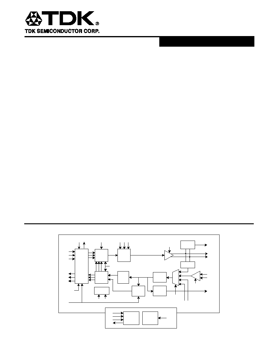
BLOCK DIAGRAM
LINN
LINP
LOUTN
LOUTP
TPOS
TNEG
TCLK
RCLK
RPOS
RNEG
DS3
TXEN
LLBKA
LLBKB
RLBK
PDTX
ENDEC
Signals from
Adjacent Port
TXNW
Control
Registers
CS
SCK
SDI
SDO
E3
LBO
Master
Bias
Generator
CKREF
Each Channel
CKREF
LOS
MON
Attenuator
Power
Distribution
B3ZS /
HDB3
Encoder
Data
Detector
B3ZS /
HDB3
Decoder
Adaptive
Equalizer
Signal
Detector
Transmit
Monitor
Pulse
Shaper
Controls
Jitter
Attenuator
Flags
TCLKP
RCLKP
Clock
Recovery
AGC
PDRX

78P2344JAT
4-port E3/DS3/STS-1 LIU
with Jitter Attenuator
- 2 -
FUNCTIONAL DESCRIPTION
The 78P2344JAT contains all the necessary
transmit and receive circuitry for connection
between E3, DS3, or STS-1 line interfaces and
digital Framer/Mapper ICs.
OPERATING RATE
The Master Control Register (MSCR) determines
which mode the device operates in according to the
table below. The MSL0 pin is also provided for
mode selection in applications without a serial
control interface. Upon power-up or reset, the state
of the MSL0 pin is sensed and mapped into the DS3
and E3 register bits representing the appropriate
mode of operation. After power-up/reset, the state of
the MSL0 pin is ignored.
Standard
MSL0 pin
DS3 bit
E3 bit
E3 L
0
1
DS3 H
1
0
STS-1 Z 0 0
STS-1 Z 1 1
RECEIVER OPERATION
The receiver input is either transformer-coupled or
capacitor-coupled to the line signal. In applications
where the highest performance and isolation are
required, a 1:1 transformer is used in the receive
path. In applications where isolation is provided
elsewhere in the circuit, capacitor coupling can be
used. The receiver input should be line terminated
externally with a termination resistor.
The AMI signal first enters an AGC, which has a
selectable gain range setting. In normal operation,
the AGC can compensate for signals with up to 6dB
of flat loss. When Receiver Monitor Mode is
enabled, the AGC can compensate for a DSX3
monitor signal with 16 to 20 dB of flat loss. The
signal then enters a high performance adaptive
equalizer. The equalizer is designed to overcome
inter-symbol interference caused by long cable
lengths. Because the equalizer is adaptive, the
circuit will work with all square-shaped signals such
as DS3-high or 34.368 Mbit/s E3. The variable gain
differential amplifier automatically controls the gain
to maintain a constant voltage level output
regardless of the input voltage level.
The outputs of the data comparators are connected
to the clock recovery circuits. The clock recovery
system employs a digital PLL, which uses a line-rate
reference clock frequency applied to the CKREF pin.
The jitter tolerance of 78P2344 meets the
requirements of ITU-T G.823 for E3 rates; the
requirements of ITU-T G.824, GR-499 (Cat I and II)
for DS3 rates; and the requirements of GR-253 for
STS1 rates.
Without the Jitter Attenuator, the jitter transfer
function meets the requirements of GR-499 for
Category II DS3 interfaces.
When the Jitter Attenuator is enabled, the
78P2344JAT meets the requirements of GR-499
and GR-253 for all categories of DS3/STS1
equipment and the ETSI TBR-24 requirements for
E3 rates. To check conformance with other
standards, please refer to the JITTER
ATTENUATOR TRANSFER FUNCTION section for
more detailed info.
RECEIVER MONITOR MODE
When in monitor mode, 20dB of flat gain is applied
to the incoming signal before it is fed to the receive
equalizer. This mode is controlled by the MON bit in
the Mode Control Register.

78P2344JAT
4-port E3/DS3/STS-1 LIU
with Jitter Attenuator
- 3 -
LOCAL LOOPBACK AND REDUNDANCY MUX
Each receiver has a 4-input MUX as shown in the
adjacent figure. In multiport applications where
redundant channels are required, the receiver MUX
can be configured to provide the necessary
multiplexing functions. This allows the user to use
one port as a redundant monitor for the other port.
The tables below show the register settings for
selecting the desired receiver input source.
LLBKA
(Port 1)
LLBKB
(Port 1)
Receiver #1 Input
Source
0 0
LINP1/LINN1
0 1
LOUTP1/LOUTN1
1 0
LINP2/LINN2
1 1
LOUTP2/LOUTN2
LLBKA
(Port 2)
LLBKB
(Port 2)
Receiver #2 Input
Source
0 0
LINP2/LINN2
0 1
LOUTP2/LOUTN2
1 0
LINP1/LINN1
1 1
LOUTP1/LOUTN1
LLBKA
(Port 3)
LLBKB
(Port 3)
Receiver #3 Input
Source
0 0
LINP3/LINN3
0 1
LOUTP3/LOUTN3
1 0
LINP4/LINN4
1 1
LOUTP4/LOUTN4
LLBKA
(Port 4)
LLBKB
(Port 4)
Receiver #4 Input
Source
0 0
LINP4/LINN4
0 1
LOUTP4/LOUTN4
1 0
LINP3/LINN3
1 1
LOUTP3/LOUTN3
Note: The LLBKA and LLBKB bits are located in the
Mode Control Register (MDCR). The Register
Control bit, REGEN, should be enabled when using
the register settings to avoid conflict with external
loopback setting pins.
Transmitter
#1
Receiver
#1
00
01
10
11
Transmitter
#2
Receiver
#2
00
01
10
11
Transmitter
#3
Receiver
#3
00
01
10
11
Transmitter
#4
Receiver
#4
00
01
10
11
LOUTP1, LOUTN1
LINP1, LINN1
LOUTP2, LOUTN2
LINP2, LINN2
LOUTP3, LOUTN3
LINP3, LINN3
LOUTP4, LOUTN4
LINP4, LINN4
LLBKA,B(1)
LLBKA,B(2)
LLBKA,B(3)
LLBKA,B(4)
When serial interface control is not available, the
respective LPBKx pin for each of the channels can
also be used to activate local loopback mode as
shown below. Note that redundant channel modes
can only be activated using the serial interface.
LPBKx
pin
Loopback Mode
L
Normal Operation
Same as LLBKA,B = `00'
Z
Remote (Digital) Loopback
Same as RLBK = `1'
H
Local (Analog) Loopback
Same as LLBKA,B = `01'

78P2344JAT
4-port E3/DS3/STS-1 LIU
with Jitter Attenuator
- 4 -
SIGNAL DETECT
When the received signal is below a minimum
threshold, the corresponding LOS signal (bit) is
asserted. A time delay is provided before this output
is active so that transient interruptions do not cause
false indications. The LOS signal can also be used
to trigger an interrupt on the INTRx pin when serial
interface control is not available. This is controlled
by setting the RXER bit in the Interrupt Control
Register (INTC).
Note: In DS3 or STS-1 mode, when LBO is not
enabled, the transmitters have to be properly
terminated to ensure reliable LOS detection. If a
transmitter is not terminated, the resultant 2x signal
is large enough to couple to the neighboring
receivers through the ESD diodes, causing false
Signal Detect indication.
B3ZS/HDB3 ENDEC WITH LINE CODE VIOLATION
DETECT
The 78P2344JAT includes a selectable B3ZS/HDB3
Encoder/Decoder (ENDEC). The ENDEC function
can be enabled or disabled through pin selection or
register setting. When the
ENDEC is enabled, the
decoder generates a composite NRZ logic data
stream following the B3ZS (for DS3/STS-1) or HDB3
(for E3) substitution codes via the RPOS pin as
shown below:
ENDEC
ENDEC
ENDEC
ENDEC
bit/pin
RPOSx RNEGx
0 / L
NRZ data
Receive Line Code
Violation Indicator
1 / H
Positive AMI
Negative AMI
The decoder also detects Receive Line Code
Violations (RLCV) and outputs a pulse via the
RNEG pin. Three different classes of line code
violations are detected.
1) Too many zeros: More than two (three)
consecutive zeros in B3ZS (HDB3) mode.
2) Not enough zeros between bipolar pulse (B)
and bipolar violation pulse (V): (B,V) for B3ZS.
(B,V) or (B,0,V) for HDB3.
3) Code violation: Even number of bipolar pulses
(B) detected between bipolar violation pulses
(V).
On the transmit side, when the ENDEC is enabled,
NRZ input data is encoded to Positive and Negative
AMI logic data following the B3ZS (for DS3/STS-1)
or HDB3 (for E3) substitution codes. The NRZ data
is input to the TPOS pin as shown below:
ENDEC
ENDEC
ENDEC
ENDEC
bit/pin
TPOSx TNEGx
0 / L
NRZ data
`Don't Care'
1 / H
Positive AMI
Negative AMI
TRANSMITTER OPERATION
Transmitters 1-4 are enabled by their corresponding
TXEN bit. When enabled, each transmitter accepts
logic level clock (TCLKx), positive data (TPOSx) and
negative data (TNEGx) signals and generates
current pulses on the LOUTPx and LOUTNx pins.
When properly connected to a 1:2CT center-tapped
transformer, an AMI pulse is generated which can
drive a 75
coaxial cable.
When the recommended transformer is used and
when DS3 mode is selected, the transmitted pulse
shape at the end of the 75
terminated cable of 0 to
450 feet will fit the DS3 template in ANSI T1.102-
1993 and Telcordia GR-499-CORE standard
documents. For STS-1 applications, the transmitted
pulse for a short cable meets the requirements of
Telcordia GR-253-CORE.
For E3 applications, the transmitted pulse for a short
cable meets the requirements of ITU-T G.703.
In either DS3 and STS-1 modes, the LBOx pin or
LBO bit should be set high for short cable (< 225 ft),
and should be set low for long cable (> 225 ft). The
LBO settings are ignored in E3 mode.
RCLK/TCLK POLARITY REVERSAL
To simplify the interface with various framer circuitry,
TCLK polarity can be internally inverted by setting
the TCLKP bit, and RCLK polarity can be inverted
by setting the RCLKP bit. Both bits are located in
the Master Control Register (MSCR).
REMOTE (DIGITAL) LOOPBACK
When the Register Control bit, REGEN, is disabled
and the LPBKx
pin is floating; or when the Register
Control bit, REGEN, is enabled and the RLBK bit is
set, RCLKx, RNEGx, and RPOSx outputs are
internally looped back to the TCLKx, TNEGx, and
TPOSx inputs respectively.

78P2344JAT
4-port E3/DS3/STS-1 LIU
with Jitter Attenuator
- 5 -
LINE BUILD-OUT
The Line Build-Out (LBO) function controls the
transmit amplitude and pulse shape in DS3 and
STS-1 modes. The selection of LBO depends on
the amount of cable the transmitter is connected to.
When less than 225 ft of cable is used, the
corresponding LBOx pin or LBO bit should be high.
When 225ft or more cable is used the corresponding
LBO setting (LBOx pin or LBO bit) should be low.
LBO can be controlled either from pins or from
register settings, depending on the status of the
Register Control bit, REGEN.
TRANSMIT ENABLE
The TXEN bit in the Mode Control Register controls
the transmitter output. When logic zero, the
transmitter output is disabled. This feature is used to
disable ports as well as to multiplex two or more
transceivers to one port. The transmitter of any port
can also be disabled by floating the respective LBOx
pin, in which case it will also power-down the entire
transmitter. See section on the Power-Down
Function for more info.
TRANSMIT MONITOR
The transmit monitor function detects activity on the
transmitter output at the LOUTPx and LOUTNx pins.
When there is a transmitter fault, in the case of an
open or short on the chip, the transformer, or the
circuit board, the transmit signal amplitude will be
altered. The transmit monitor detects the amplitude
of the driven signal. The TXNW signal (bit) goes
high when the amplitude of the transmit signal is
outside a valid amplitude range. When the signal
amplitude is either too high or too low for longer than
a specified duration, the TXNW bit goes high. The
TXNW signal can be also used to trigger an interrupt
on the INTRx pin when serial interface control is not
available. This is accomplished by setting the TXER
bit in the Interrupt Control Register (INTC).
JITTER ATTENUATOR
Jitter Attenuation function is provided on-chip. The
Jitter Attenuator can be configured to be in the
transmit or the receive path. When configured in the
transmit path, the input clock at TCLK pin is passed
through a very low bandwidth digital PLL. The
corresponding transmit data is buffered into a FIFO
and clocked out using the de-jittered output clock of
the PLL. When configured in the receive path, the
recovered clock is passed through the low
bandwidth digital PLL, and the corresponding
receive data is buffered into the FIFO and clocked
out using the de-jittered clock.
The Jitter Attenuator can be configured
independently for each channel by writing to the
Jitter Attenuator Control Register (JACR) as follows:
JAEN
bit
JASL
bit
Jitter Attenuator Mode
0
X
Jitter Attenuator disabled
1
0
Jitter Attenuator configured
to be in the receive path
1
1
Jitter Attenuator configured
to be in the transmit path
When serial interface control is not available, the
MSL1 pin is provided for Jitter Attenuator mode
selection. Upon power-up or reset, the state of the
MSL1 pin is sensed and mapped into the JAEN and
JASL register bits for all channels, representing the
appropriate mode of operation. After power-up or
reset, the state of the MSL1 pin is ignored. The
state of the MSL1 pin, and the corresponding Jitter
Attenuator configuration is shown below.
MSL1 pin
Jitter Attenuator Mode
L
Jitter Attenuator in receive path
H
Jitter Attenuator in transmit path
Z
Jitter Attenuator disabled
PLL Bandwidth
A PLL response with effectively one pole below 27
Hz is adequate to meet the ETSI TBR24 E3
standards. A PLL response with one pole below 40
Hz is adequate to meet the GR-499 (Cat I) DS3
standards. Either of the two bandwidths can be
selected via register setting. In either high or low
bandwidth mode, the PLL bandwidth is proportional
to the data rate as follows:
Line Rate
JABW bit
PLL Bandwidth (Hz)
0 13
E3
1 188
0 17
DS3
1 245
0 20
STS1
1 283
The default state of the JABW bit depends on which
line-rate is selected through the MSL0 pin. If E3 or
DS3 mode is selected, the default state is `0'. If
STS1 mode is selected, the default state is `1'.