 | –≠–ª–µ–∫—Ç—Ä–æ–Ω–Ω—ã–π –∫–æ–º–ø–æ–Ω–µ–Ω—Ç: TC4428MJA | –°–∫–∞—á–∞—Ç—å:  PDF PDF  ZIP ZIP |
Document Outline
- Return to Contents
- Features
- Ordering Information
- General Description
- Functional Block Diagram
- Absolute Maximum Ratings*
- Pin Configurations
- Electrical Characteristics: TA = +25∞C with 4.5V £ VDD £ 18V, unless otherwise specified.
- Typical Characteristics
- Supply Current Characteristics (Load on Single Output Only)
4-245
TELCOM SEMICONDUCTOR, INC.
7
6
5
4
3
1
2
8
1.5A DUAL HIGH-SPEED, POWER MOSFET DRIVERS
TC4426
TC4427
TC4428
OUTPUT
INPUT
GND
EFFECTIVE INPUT
C = 12 pF
300 mV
INVERTING
OUTPUTS
NONINVERTING
OUTPUTS
V
DD
TC4426/TC4427/TC4428
4.7V
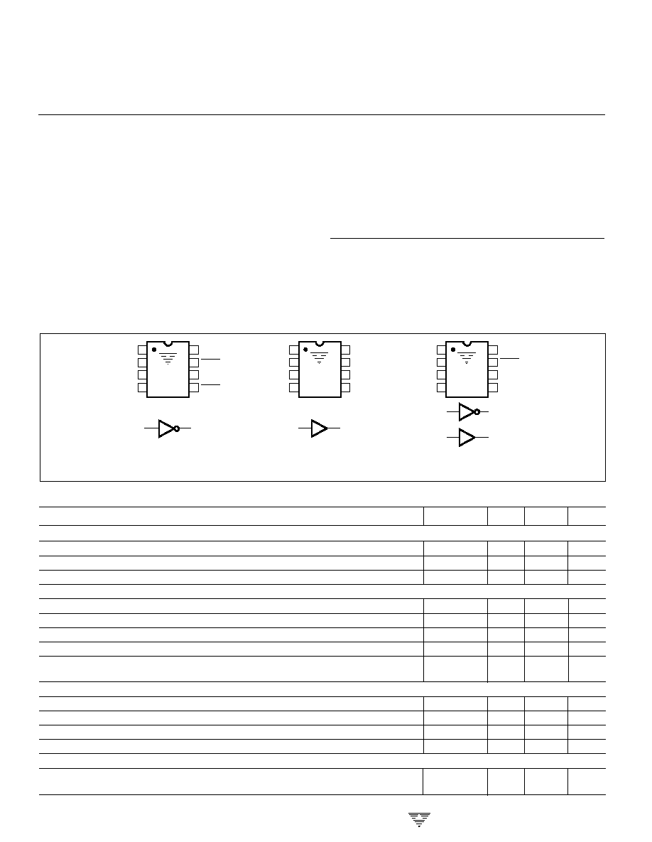
NOTES: 1.TC4426 has 2 inverting drivers; TC4427 has 2 noninverting drivers.
2. TC4428 has one inverting and one noninverting driver.
3. Ground any unused driver input.
FEATURES
s
High Peak Output Current ............................... 1.5A
s
Wide Operating Range .......................... 4.5V to 18V
s
High Capacitive Load
Drive Capability ........................ 1000 pF in 25 nsec
s
Short Delay Time ................................ <40nsec Typ
s
Consistent Delay Times With Changes in
Supply Voltage
s
Low Supply Current
-- With Logic "1" Input .................................... 4mA
-- With Logic "0" Input ................................. 400
µ
A
s
Low Output Impedance ....................................... 7
s
Latch-Up Protected: Will Withstand >0.5A
Reverse Current ................................. Down to ≠ 5V
s
Input Will Withstand Negative Inputs
s
ESD Protected ..................................................... 4kV
s
Pinout Same as TC426/TC427/TC428
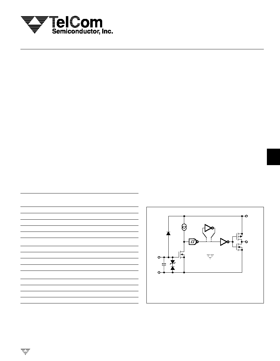
GENERAL DESCRIPTION
The TC4426/4427/4428 are improved versions of the
earlier TC426/427/428 family of buffer/drivers (with which
they are pin compatible). They will not latch up under any
conditions within their power and voltage ratings. They are
not subject to damage when up to 5V of noise spiking (of
either polarity) occurs on the ground pin. They can accept,
without damage or logic upset, up to 500mA of reverse
current (of either polarity) being forced back into their
outputs. All terminals are fully protected against up to 4kV of
electrostatic discharge.
As MOSFET drivers, the TC4426/4427/4428 can easily
switch 1000 pF gate capacitances in under 30nsec, and
provide low enough impedances in both the ON and OFF
states to ensure the MOSFET's intended state will not be
affected, even by large transients.
Other compatible drivers are the TC4426A/27A/28A.
These drivers have matched input to output leading edge
and falling edge delays, tD1 and tD2, for processing short
duration pulses in the 25 nanoseconds range. They are pin
compatible with the TC4426/27/28.
TC4426/7/8-8 10/21/96
FUNCTIONAL BLOCK DIAGRAM
ORDERING INFORMATION
Temperature
Part No.
Package
Range
TC4426COA
8-Pin SOIC
0
∞
C to +70
∞
C
TC4426CPA
8-Pin Plastic DIP
0
∞
C to +70
∞
C
TC4426EOA
8-Pin SOIC
≠ 40
∞
C to +85
∞
C
TC4426EPA
8-Pin Plastic DIP
≠ 40
∞
C to +85
∞
C
TC4426MJA
8-Pin CerDIP
≠ 55
∞
C to +125
∞
C
TC4427COA
8-Pin SOIC
0
∞
C to +70
∞
C
TC4427CPA
8-Pin Plastic DIP
0
∞
C to +70
∞
C
TC4427EOA
8-Pin SOIC
≠ 40
∞
C to +85
∞
C
TC4427EPA
8-Pin Plastic DIP
≠ 40
∞
C to +85
∞
C
TC4427MJA
8-Pin CerDIP
≠ 55
∞
C to +125
∞
C
TC4428COA
8-Pin SOIC
0
∞
C to +70
∞
C
TC4428CPA
8-Pin Plastic DIP
0
∞
C to +70
∞
C
TC4428EOA
8-Pin SOIC
≠ 40
∞
C to +85
∞
C
TC4428EPA
8-Pin Plastic DIP
≠ 40
∞
C to +85
∞
C
TC4428MJA
8-Pin CerDIP
≠ 55
∞
C to +125
∞
C
4-246
TELCOM SEMICONDUCTOR, INC.
1.5A DUAL HIGH-SPEED
POWER MOSFET DRIVERS
TC4426
TC4427
TC4428
ABSOLUTE MAXIMUM RATINGS*
Supply Voltage ......................................................... +22V
Input Voltage, IN A or IN B . (V
DD
+ 0.3V) to (GND ≠ 5.0V)
Maximum Chip Temperature ................................. +150
∞
C
Storage Temperature Range ................ ≠ 65
∞
C to +150
∞
C
Lead Temperature (Soldering, 10 sec) ................. +300
∞
C
Package Thermal Resistance
CerDIP R
J-A
................................................ 150
∞
C/W
CerDIP R
J-C
.................................................. 50
∞
C/W
PDIP R
J-A
................................................... 125
∞
C/W
PDIP R
J-C
..................................................... 42
∞
C/W
SOIC R
J-A
................................................... 155
∞
C/W
SOIC R
J-C
..................................................... 45
∞
C/W
Operating Temperature Range
C Version ............................................... 0
∞
C to +70
∞
C
E Version .......................................... ≠ 40
∞
C to +85
∞
C
M Version ....................................... ≠ 55
∞
C to +125
∞
C
Package Power Dissipation (T
A
70
∞
C)
Plastic ............................................................. 730mW
CerDIP ............................................................ 800mW
SOIC ...............................................................470mW
*Static-sensitive device. Unused devices must be stored in conductive
material. Protect devices from static discharge and static fields. Stresses
above those listed under "Absolute Maximum Ratings" may cause perma-
nent damage to the device. These are stress ratings only and functional
operation of the device at these or any other conditions above those
indicated in the operation sections of the specifications is not implied.
Exposure to absolute maximum rating conditions for extended periods may
affect device reliability.
ELECTRICAL CHARACTERISTICS:
T
A
= +25
∞
C with 4.5V
V
DD
18V, unless otherwise specified.
Symbol
Parameter
Test Conditions
Min
Typ
Max
Unit
Input
V
IH
Logic 1 High Input Voltage
2.4
--
--
V
V
IL
Logic 0 Low Input Voltage
--
--
0.8
V
I
IN
Input Current
0V
V
IN
V
DD
≠ 1
--
1
µ
A
Output
V
OH
High Output Voltage
V
DD
≠ 0.025
--
--
V
V
OL
Low Output Voltage
--
--
0.025
V
R
O
Output Resistance
V
DD
= 18V, I
O
= 10 mA
--
7
10
I
PK
Peak Output Current
Duty Cycle
2%, t
30
µ
sec
--
1.5
--
A
I
REV
Latch-Up Protection
Duty Cycle
2%
> 0.5
--
--
A
Withstand Reverse Current
t
30
µ
sec
Switching Time (Note 1)
t
R
Rise Time
Figure 1
--
19
30
nsec
t
F
Fall Time
Figure 1
--
19
30
nsec
t
D1
Delay Time
Figure 1
--
20
30
nsec
t
D2
Delay Time
Figure 1
--
40
50
nsec
Power Supply
I
S
Power Supply Current
V
IN
= 3V (Both Inputs)
--
--
4.5
mA
V
IN
= 0V (Both Inputs)
--
--
0.4
mA
NOTE: 1. Switching times are guaranteed by design.
PIN CONFIGURATIONS
TC4426
1
2
3
4
NC
5
6
7
8
OUT A
OUT B
NC
IN A
GND
IN B
V
DD
NC = NO INTERNAL CONNECTION
TC4427
1
2
3
4
NC
5
6
7
8
OUT A
OUT B
NC
IN A
GND
IN B
TC4428
1
2
3
4
NC
5
6
7
8
OUT A
OUT B
NC
IN A
GND
IN B
2,4
7,5
INVERTING
2,4
7,5
NONINVERTING
VDD
2
4
DIFFERENTIAL
7
5
VDD
NOTE: SOIC pinout is identical to DIP.

4-247
TELCOM SEMICONDUCTOR, INC.
7
6
5
4
3
1
2
8
1.5A DUAL HIGH-SPEED
POWER MOSFET DRIVERS
TC4426
TC4427
TC4428
ELECTRICAL CHARACTERISTICS (CONT.):
Specifications measured over operating temperature
range with 4.5V
V
DD
18V, unless otherwise specified.
Symbol
Parameter
Test Conditions
Min
Typ
Max
Unit
Input
V
IH
Logic 1 High Input Voltage
2.4
--
--
V
V
IL
Logic 0 Low Input Voltage
--
--
0.8
V
I
IN
Input Current
0V
V
IN
V
DD
≠ 10
--
10
µ
A
Output
V
OH
High Output Voltage
V
DD
≠ 0.025
--
--
V
V
OL
Low Output Voltage
--
--
0.025
V
R
O
Output Resistance
V
DD
= 18V, I
O
= 10 mA
--
9
12
I
PK
Peak Output Current
Duty Cycle
2%, t
300
µ
sec
--
1.5
--
A
I
REV
Latch-Up Protection
Duty Cycle
2%
> 0.5
--
--
A
Withstand Reverse Current
t
300
µ
sec
Switching Time (Note 1)
t
R
Rise Time
Figure 1
--
--
40
nsec
t
F
Fall Time
Figure 1
--
--
40
nsec
t
D1
Delay Time
Figure 1
--
--
40
nsec
t
D2
Delay Time
Figure 1
--
--
60
nsec
Power Supply
I
S
Power Supply Current
V
IN
= 3V (Both Inputs)
--
--
8
mA
V
IN
= 0V (Both Inputs)
--
--
0.6
NOTE: 1. Switching times are guaranteed by design.
+5V
INPUT
10%
90%
10%
90%
10%
90%
VDD
OUTPUT
tD1
0V
90%
10%
10%
10%
t
F
90%
+5V
INPUT
VDD
OUTPUT
0V
0V
0V
90%
OUTPUT
INPUT
0.1 µF
CL = 1000 pF
4.7 µF
VDD= 18V
Inverting Driver
3
2,4
5,7
6
Noninverting Driver
tF
tD2
tR
tR
tD1
tD2
INPUT: 100 kHz, square wave,
tRISE = tFALL
10ns
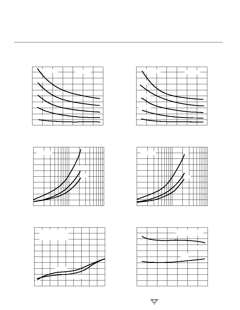
Figure 1. Switching Time Test Circuit
NOTE: The values on this graph represent the loss seen by both drivers in a package
during one complete cycle. For a single driver, divide the stated values by 2. For a
single transition of a single driver, divide the stated value by 4.
200
0
400
600
800
1000
1200
1400
1600
0
10
20
30
40
50
60
70
80
90
100
110
120
AMBIENT TEMPERATURE (
∞
C)
MAX. POWER (mW)
8 Pin DIP
Thermal Derating Curves
8 Pin CerDIP
8 Pin SOIC
Crossover Energy Loss
4
A ∑ sec
18
6
8
10
12
14
16
8
7
6
5
4
3
2
10
≠9
10
≠8
9
V
DD
4-248
TELCOM SEMICONDUCTOR, INC.
TYPICAL CHARACTERISTICS
Rise TIme vs. Capacitive Load
TIME (nsec)
Rise and Fall Times vs. Temperature
tRISE
TEMPERATURE (
∞
C)
C = 1000 pF
LOAD
V = 17.5V
DD
Propagation Delay vs. Supply Voltage
t FALL
(nsec)
4
6
8
10
12
14
16
18
Fall Time vs. Supply Voltage
100 pF
470 pF
1000 pF
2200 pF
1500 pF
t RISE
(nsec)
4
6
8
10
12
14
16
18
Rise Time vs. Supply Voltage
VDD
100 pF
470 pF
2200 pF
T
A
= 25
∞
C
T
A
= 25
∞
C
1500 pF
100
1000
10,000
C (pF)
LOAD
5V
10V
15V
Fall TIme vs. Capacitive Load
100
1000
10,000
5V
10V
60
≠55 ≠35
5
25
45
65
85
105 125
≠15
60
4
6
8
10
12
14
16
18
DELAY TIME (nsec)
t D2
tD1
C = 1000 pF
LOAD
100
VDD
C (pF)
LOAD
tFALL
VDD
1000 pF
80
60
40
20
0
100
80
60
40
20
0
100
80
60
40
20
0
100
80
60
40
20
0
50
40
30
20
10
50
40
30
20
10
t RISE
(nsec)
t FALL
(nsec)
15V
T
A
= 25
∞
C
T
A
= 25
∞
C
T
A
= 25
∞
C
1.5A DUAL HIGH-SPEED
POWER MOSFET DRIVERS
TC4426
TC4427
TC4428

4-249
TELCOM SEMICONDUCTOR, INC.
7
6
5
4
3
1
2
8
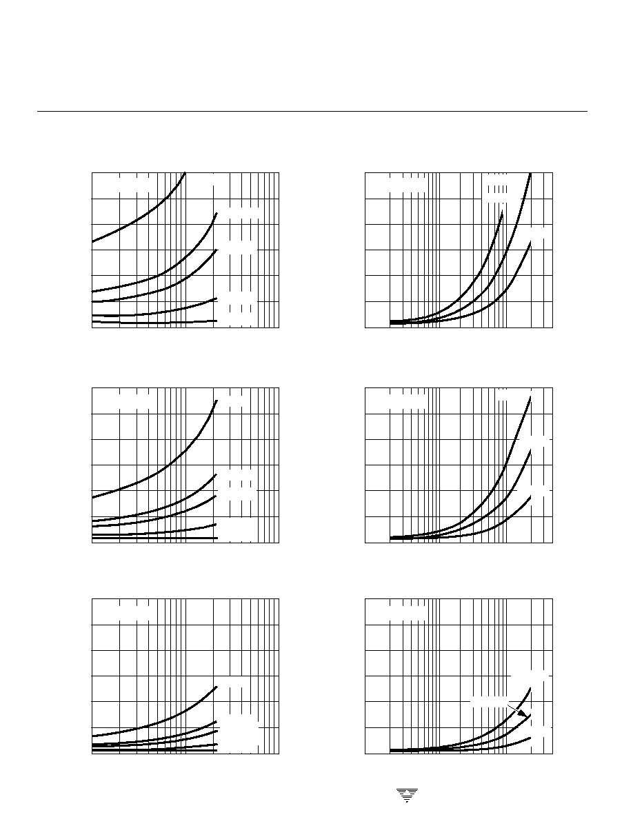
TYPICAL CHARACTERISTICS (Cont.)
Quiescent Supply Current vs. Voltage
High-State Output Resistance
TA (
∞
C)
4
TA (
∞
C)
I QUIESCENT
(mA)
4.0
3.5
3.0
2.5
2.0
I (mA) QUIESCENT
18
6
8
10
12
14
16
DELAY TIME (nsec)
VDRIVE (V)
60
0.1
≠55 ≠35 ≠15
5
25
45
65
85
105 125
Quiescent Supply Current vs. Temperature
Effect of Input Amplitude on Delay Time
Propagation Delay Time vs. Temperature
4
6
8
10
12
14
16
18
4
6
8
10
12
14
16
18
20
Low-State Output Resistance
≠55 ≠35 ≠15
5
25
45
65
85
105 125
C = 1000 pF
LOAD
V = 10V
DD
T = +25
∞
C
A
V = 1000 pF
LOAD
V = 18V
DD
tD2
tD2
BOTH INPUTS = 1
BOTH INPUTS = 0
0
2
4
6
8
10
tD1
V
DD
V
DD
V
DD
50
40
30
20
10
DELAY TIME (nsec)
60
50
40
30
20
10
1
25
15
10
8
5
R
DS(ON)
(
)
20
25
15
10
8
5
tD1
WORST CASE @ TJ = +150
∞
C
TYP @ TA = +25
∞
C
WORST CASE @ TJ = +150
∞
C
TYP @ TA = +25
∞
C
R
DS(ON)
(
)
V = 18V
DD
BOTH INPUTS = 1
1.5A DUAL HIGH-SPEED
POWER MOSFET DRIVERS
TC4426
TC4427
TC4428
4-250
TELCOM SEMICONDUCTOR, INC.
SUPPLY CURRENT CHARACTERISTICS (Load on Single Output Only)
Supply Current vs. Capacitive Load
60
100
1000
10,000
I SUPPLY
(mA)
Supply Current vs. Capacitive Load
100
1000
10,000
Supply Current vs. Capacitive Load
100
1000
10,000
Supply Current vs. Frequency
10
100
1000
FREQUENCY (kHz)
Supply Current vs. Frequency
10
100
1000
FREQUENCY (kHz)
Supply Current vs. Frequency
10
100
1000
FREQUENCY (kHz)
2 MHz
600 kHz
200 kHz
20 kHz
900 kHz
2 MHz
600 kHz
200 kHz
20 kHz
900 kHz
2 MHz
200 kHz
20 kHz
600 kHz
900 kHz
1000 pF
2200 pF
1000 pF
2200 pF
100 pF
1000 pF
2200 pF
100 pF
V = 18V
DD
V = 12V
DD
V = 12V
DD
V = 6V
DD
V = 6V
DD
100 pF
C (pF)
LOAD
C (pF)
LOAD
C (pF)
LOAD
V = 18V
DD
50
40
30
20
10
0
60
50
40
30
20
10
0
60
50
40
30
20
10
0
60
50
40
30
20
10
0
60
50
40
30
20
10
0
60
50
40
30
20
10
0
I SUPPLY
(mA)
I SUPPLY
(mA)
I SUPPLY
(mA)
I SUPPLY
(mA)
I SUPPLY
(mA)
1.5A DUAL HIGH-SPEED
POWER MOSFET DRIVERS
TC4426
TC4427
TC4428