 | –≠–ª–µ–∫—Ç—Ä–æ–Ω–Ω—ã–π –∫–æ–º–ø–æ–Ω–µ–Ω—Ç: TC4431EOA | –°–∫–∞—á–∞—Ç—å:  PDF PDF  ZIP ZIP |
Document Outline
- Return to Contents
- List of Figures
- 1. Switching Time Test Circuit
- Features
- Ordering Information
- Functional Block Diagram
- General Description
- Absolute Maximum Ratings*
- Electrical Characteristics: TA = +25∞C with 5.0 £ VDD £ 30V, unless otherwise specified.
- Pin Configurations
- Typical Characteristics

4-257
TELCOM SEMICONDUCTOR, INC.
7
6
5
4
3
1
2
8
1.5A HIGH-SPEED 30V MOSFET DRIVERS
FEATURES
s
High Peak Output Current ............................... 1.5A
s
Wide Operating Range ............................. 5V to 30V
s
High Capacitive Load
Drive Capability ......................... 1000 pF in 25nsec
s
Short Delay Time ................................ <78nsec Typ
s
Low Supply Current
-- With Logic "1" Input ................................. 2.5mA
-- With Logic "0" Input ................................. 300
µ
A
s
Low Output Impedance ....................................... 7
s
Latch-Up Protected .......... Will Withstand >300mA
Reverse Current
s
ESD Protected .................................................... 4 kV
TC4431
TC4432
GENERAL DESCRIPTION
The TC4431/4432 are 30V CMOS buffer/drivers suit-
able for use in high-side driver applications. They will not
latch up under any conditions within their power and voltage
ratings. They can accept, without damage or logic upset, up
to 300mA of reverse current (of either polarity) being forced
back into their outputs. All terminals are fully protected
against up to 4kV of electrostatic discharge.
Under-voltage lockout circuitry forces the output to a
"low" state when the input supply voltage drops below 7V.
Maximum startup V
DD
bias voltage threshold is 10V. For
operation at lower voltages, the LOCK DIS, Pin 3 can be
grounded to disable the lockout and start-up circuit. The
under-voltage lockout and start-up circuit gives brown out
protection when driving MOSFETS.
ORDERING INFORMATION
Temperature
Part No.
Package
Range
TC4431COA
8-Pin SOIC
0
∞
C to +70
∞
C
TC4431CPA
8-Pin Plastic DIP
0
∞
C to +70
∞
C
TC4431EJA
8-Pin CerDIP
≠ 40
∞
C to +85
∞
C
TC4431EOA
8-Pin SOIC
≠ 40
∞
C to +85
∞
C
TC4431EPA
8-Pin Plastic DIP
≠ 40
∞
C to +85
∞
C
Temperature
Part No.
Package
Range
TC4432COA
8-Pin SOIC
0
∞
C to +70
∞
C
TC4432CPA
8-Pin Plastic DIP
0
∞
C to +70
∞
C
TC4432EJA
8-Pin CerDIP
≠ 40
∞
C to +85
∞
C
TC4432EOA
8-Pin SOIC
≠ 40
∞
C to +85
∞
C
TC4432EPA
8-Pin Plastic DIP
≠ 40
∞
C to +85
∞
C
FUNCTIONAL BLOCK DIAGRAM
2 mA
OUT
INPUT
GND
EFFECTIVE
INPUT
C = 10pF
V
DD
TC4431/32
Inverting/Noninverting
OUT
UV LOCK
Inverted
TC4431
250mV
LOCK DIS.
3
2
4, 5
Non-Inverted
TC4432
6
7
8
TC4431/2-8 10/21/96

4-258
TELCOM SEMICONDUCTOR, INC.
1.5A HIGH-SPEED 30V MOSFET DRIVERS
TC4431
TC4431
ELECTRICAL CHARACTERISTICS:
T
A
= +25
∞
C with 5.0
V
DD
30V, unless otherwise specified.
Symbol
Parameter
Test Conditions
Min
Typ
Max
Unit
Input
V
IH
Logic 1 High Input Voltage
2.4
--
--
V
V
IL
Logic 0 Low Input Voltage
--
--
0.8
V
I
IN
Input Current (Note 1)
0V
V
IN
V
DD
(16V MAX)
≠1
--
1
µ
A
Output
V
OH
High Output Voltage
I
OUT
= 100mA
V
DD
≠ 1.0
V
DD
≠ 0.8
--
V
V
OL
Low Output Voltage
--
--
0.025
V
R
O
Output Resistance (V
OL
)
V
DD
= 30V, I
O
= 10mA
--
7
10
I
PK
Peak Output Current
Source: V
DD
= 30V
--
3.0
--
A
Sink: V
DD
= 30V
--
1.5
--
I
REV
Latch-Up Protection
Duty Cycle
2%
0.3
--
--
A
Withstand Reverse Current
t
300
µ
sec
Switching Time (Note 2)
t
R
Rise Time
Figure 1
--
25
40
nsec
t
F
Fall Time
Figure 1
--
33
50
nsec
t
D1
Delay Time
Figure 1
--
62
80
nsec
t
D2
Delay Time
Figure 1
--
78
90
nsec
Power Supply
I
S
Power Supply Current
V
IN
= 3V
--
2.5
4
mA
V
IN
= 0V
--
0.3
0.4
V
S
Start-up Threshold
--
8.4
10
V
V
DO
Drop-out Threshold
(Note 3)
7
7.7
--
V
ABSOLUTE MAXIMUM RATINGS*
Supply Voltage ............................................................36V
Input Voltage (Note 1) ........................ V
DD
+ 0.3V to GND
Maximum Chip Temperature ................................. +150
∞
C
Storage Temperature Range ................ ≠ 65
∞
C to +150
∞
C
Lead Temperature (Soldering, 10 sec) ................. +300
∞
C
Package Thermal Resistance
CerDIP R
J-A
................................................ 150
∞
C/W
CerDIP R
J-C
.................................................. 50
∞
C/W
PDIP R
J-A
................................................... 125
∞
C/W
PDIP R
J-C
..................................................... 42
∞
C/W
SOIC R
J-A
................................................... 250
∞
C/W
SOIC R
J-C
..................................................... 75
∞
C/W
*Static-sensitive device. Unused devices must be stored in conductive
material. Protect devices from static discharge and static fields. Stresses
above those listed under "Absolute Maximum Ratings" may cause perma-
nent damage to the device. These are stress ratings only and functional
operation of the device at these or any other conditions above those
indicated in the operation sections of the specifications is not implied.
Exposure to absolute maximum rating conditions for extended periods may
affect device reliability.
Operating Temperature Range
C Version ............................................... 0
∞
C to +70
∞
C
E Version ........................................... - 40
∞
C to +85
∞
C
Package Power Dissipation (T
A
70
∞
C )
Plastic ............................................................. 730mW
CerDIP ............................................................ 800mW
SOIC ............................................................... 470mW

4-259
TELCOM SEMICONDUCTOR, INC.
7
6
5
4
3
1
2
8
1.5A HIGH-SPEED 30V MOSFET DRIVERS
TC4431
TC4432
ELECTRICAL CHARACTERISTICS (Cont.):
Specifications measured over operating temperature range
with 5.0V
V
DD
30V, unless otherwise specified.
Symbol
Parameter
Test Conditions
Min
Typ
Max
Unit
Input
V
IH
Logic 1 High Input Voltage
2.4
--
--
V
V
IL
Logic 0 Low Input Voltage
--
--
0.8
V
I
IN
Input Current (Note 1)
0V
V
IN
V
DD
(16V MAX)
≠ 1
--
1
µ
A
Output
V
OH
High Output Voltage
I
OUT
= 100mA
V
DD
≠ 1.2
--
--
V
V
OL
Low Output Voltage
--
--
0.025
V
R
O
Output Resistance
V
DD
= 30V, I
O
= 10mA
--
--
12
Switching Time (Note 2)
t
R
Rise Time
Figure 1
--
--
60
nsec
t
F
Fall Time
Figure 1
--
--
70
nsec
t
D1
Delay Time
Figure 1
--
--
100
nsec
t
D2
Delay Time
Figure 1
--
--
110
nsec
Power Supply
I
S
Power Supply Current
V
IN
= 3V
--
--
6
mA
V
IN
= 0V
--
--
0.7
V
S
Start-up Threshold
--
8.4
10
V
V
DO
Drop-out Threshold
(Note 3)
7
7.7
--
V
NOTES: 1. For inputs >16V, add a 1k
resistor in series with the input. See graph on page 4 for input current.
2. Switching times are guaranteed by design.
3. For operation below 7V, the LOCK DIS., Pin 3 can be grounded to disable the lockout and start-up circuit.
PIN CONFIGURATIONS
TC4431
1
2
3
4
VDD
5
6
7
8
OUT
GND
VDD
IN
LOCK DIS
GND
TC4432
1
2
3
4
VDD
5
6
7
8
OUT
GND
VDD
IN
GND
2
7
INVERTING
NONINVERTING
OUT
NOTE: SOIC pinout is identical to DIP.
OUT
6
LOCK DIS
2
7
6
4-260
TELCOM SEMICONDUCTOR, INC.
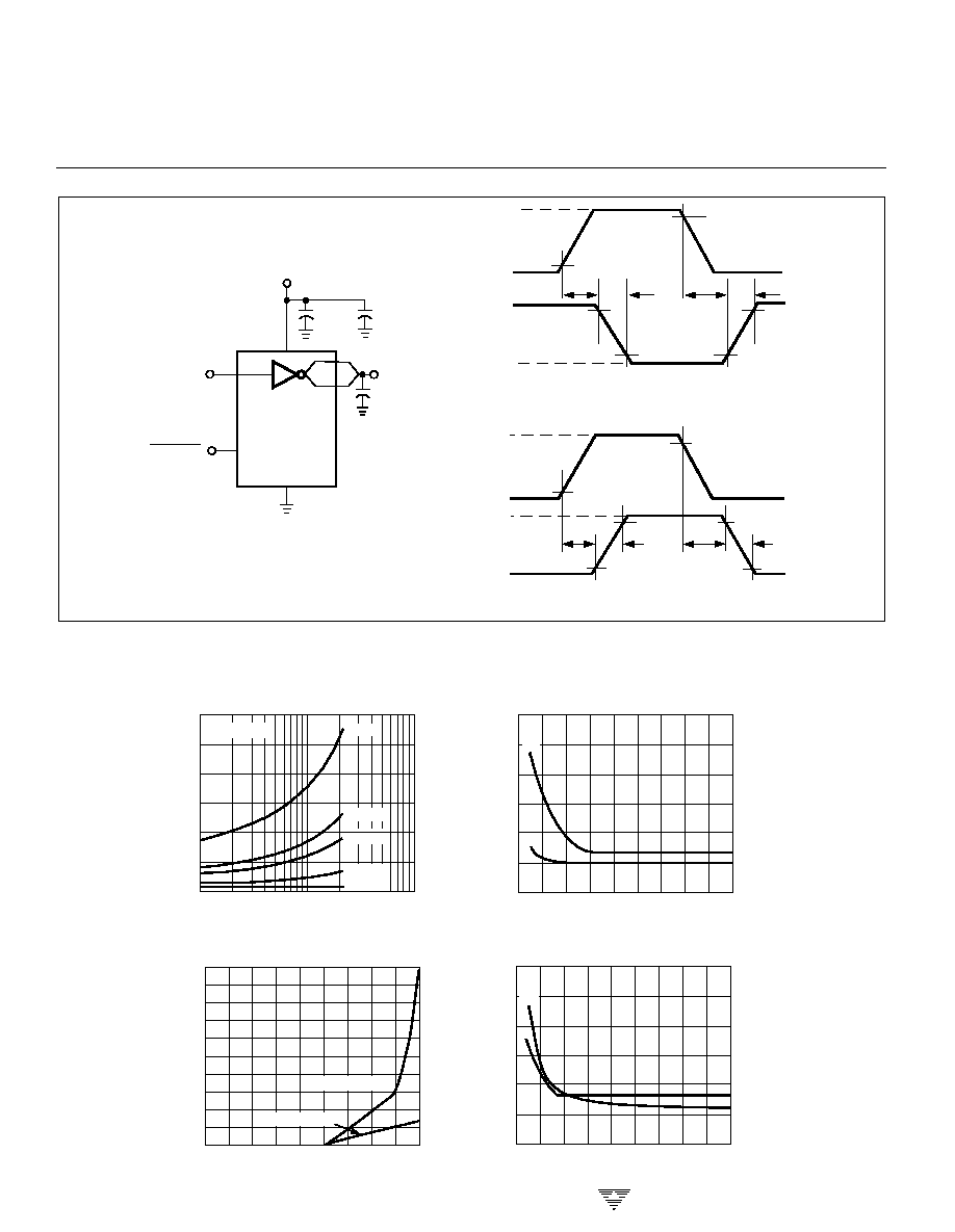
+5V
INPUT
10%
90%
10%
90%
10%
90%
VDD
OUTPUT
tD1
0V
0V
90%
10%
10%
10%
t
F
90%
+5V
INPUT
VDD
OUTPUT
0V
0V
90%
OUTPUT
INPUT
0.1
µ
F
CL = 1000 pF
4.7
µ
F
VDD= 30V
Inverting Driver
4, 5
2
7
Noninverting Driver
tF
tD2
tR
tR
tD1
tD2
INPUT: 100 kHz, square wave,
tRISE = tFALL
10nsec
1, 8
6
3
LOCK DIS.
Supply Current vs. Capacitive Load
100
1000
10,000
2 MHz
600 kHz
200 kHz
20 kHz
900 kHz
V = 12V
DD
C (pF)
LOAD
60
50
40
30
20
10
0
I SUPPLY
(mA)
Input Curent (mA)
Input Current vs. Input Voltage
Input Voltage (VIN)
50
3
6
12
15
18
21
24
27
30
9
40
30
20
10
0
WITHOUT 1K RES.
45
35
25
15
5
WITH 1K RES.
Time (nsec)
Rise/Fall Time vs. VDD
CLOAD = 1000pf at 25 C
VDD (VOLTS)
3
6
12
15
18
21
24
27
30
9
150
125
100
75
50
25
0
TR
Time (nsec)
TD1 and TD2 Delay vs. VDD
CLOAD = 1000pf at 25 C
VDD (VOLTS)
3
6
12
15
18
21
24
27
30
9
300
250
200
150
100
50
0
TD2
TD1
TF
Figure 1. Switching Time Test Circuit
TYPICAL CHARACTERISTICS
1.5A HIGH-SPEED 30V MOSFET DRIVERS
TC4431
TC4431