Document Outline
- Return to Contents
- List of Figures
- 1. Serial Port Timing
- 2. A/D Converter Timing
- 3. Integrating Converter Normal Mode Rejection
- 4. TC530/534 Initialization and Load Value Write Cycle
- 5. Serial Port Data Read Cycle
- 6. TC530/534 Typical Application
- List of Tables
- 1. CREF and CAZ Selection
- 2. Recommend Capacitor for CINT
- Features
- Ordering Information
- Functional Block Diagram
- General Description
- Absolute Maximum Ratings*
- Electrical Characteristics
- Electrical Characteristics: VDD = VCCD, CAZ = CREF = 0.47mF, unless otherwise specified.
- Electrical Characteristics: Serial Port Interface: +5V, unless otherwise specified.
- Electrical Characteristics: Serial Port Interface: VCCD = +5V, unless otherwise specified.
- Electrical Characteristics: DC/DC Converter Section
- Electrical Characteristics: Multiplexer
- Pin Configurations
- Pin Description
- Detailed Description
- Dual Slope Integrating Converter
- Applications
- Programming the TC530/534
- Selecting Component Values for the TC530/534
- Applications
- Design Example
- Power Supply Sequencing
- Circuit Design/Layout Considerations
- TC530EV Evaluation Kit
- Typical Characteristics
- WIMA Corporation Capacitor Representatives

3-47
TELCOM SEMICONDUCTOR, INC.
7
6
5
4
3
1
2
8
TC530
TC534
5V PRECISION DATA ACQUISITION SUBSYSTEMS
EVALUATION
KIT
AVAILABLE
TC530/534-3 11/14/96
FEATURES
s
Precision (up to 17 Bits) A/D Converter
s
3 Wire Serial Port
s
Flexible: User Can Trade-Off Conversion Speed
Against Resolution
s
Single Supply Operation
s
�5V Output Pin
s
4 Input, Differential Analog MUX (TC534)
s
Automatic Input Polarity and Overrange Detection
s
Low Operating Current ............................ 5mA Max
s
Wide Analog Input Range ......................
�
4.2V Max
s
Cost Effective
ORDERING INFORMATION
Part No.
Package
Temp. Range
TC530COI
28-Pin SOIC
0
�
C to +70
�
C
TC530CPJ
28-Pin Plastic DIP (300 Mil.)
0
�
C to +70
�
C
TC534CKW
44-Pin PQFP
0
�
C to +70
�
C
TC534CPL
40-Pin Plastic DIP
0
�
C to +70
�
C
TC530EV
Evaluation Kit for TC530/534
FUNCTIONAL BLOCK DIAGRAM
GENERAL DESCRIPTION
The TC530/534 are serial analog data acquisition sub-
systems ideal for high precision measurements (up to 17 bits
plus sign). The TC530 consists of a dual slope integrating
A/D converter, negative power supply generator and 3 wire
serial interface port. The TC534 is identical to the TC530, but
adds a four channel differential input multiplexer. Key A/D
converter operating parameters (Auto Zero and Integration
time) are programmable, allowing the user to trade-off
conversion time for resolution.
Data conversion is initiated when the RESET input is
brought low. After conversion, data is loaded into the output
shift register and EOC is asserted indicating new data is
available. The converted data (plus Overrange and polarity
bits) is held in the output shift register until read by the
processor, or until the next conversion is completed allowing
the user to access data at any time.
The TC530/534 timebase can be derived from an exter-
nal crystal of 2MHz (max), or from an external frequency
source. The TC530/534 requires a single 5V power supply
and features a � 5V, 10mA output which can be used to
supply negative bias to other components in the system.
A0 A1
OSC
IN
EOC
R/W
D
IN
D
OUT
D
CLK
OSC
OUT
OSC
RESET
CAP
+
CAP
�
C
AZ
TC05
TC530
TC534
C
REF
R
INT
C
INT
TC534
(Only)
(TC530 Only)
DC-TO-DC
CONVERTER
State
Machine
Serial Port
Negative
Supply Output
Oscillator
(
�
4)
Dual Slope A/D Converter
.01
�
F
0.01
�
F
Optional
Power-On
Reset Cap
100k
10k
+5V
DIF.
MUX
(TC534
Only)
CH1
CH1
CH2
CH2
CH3
CH3
CH4
CH4
V
IN
V
IN
IN
IN
A
B
CMPTR
BUF
INT
C
AZ
V
REF
+
V
REF
�
+
C
REF
C
REF
�
ACOM
�
�
�
�
�
+
+
+
+
+
V
DD
V
DD
V
DD
V
DD
V
SS
+
�

3-48
TELCOM SEMICONDUCTOR, INC.
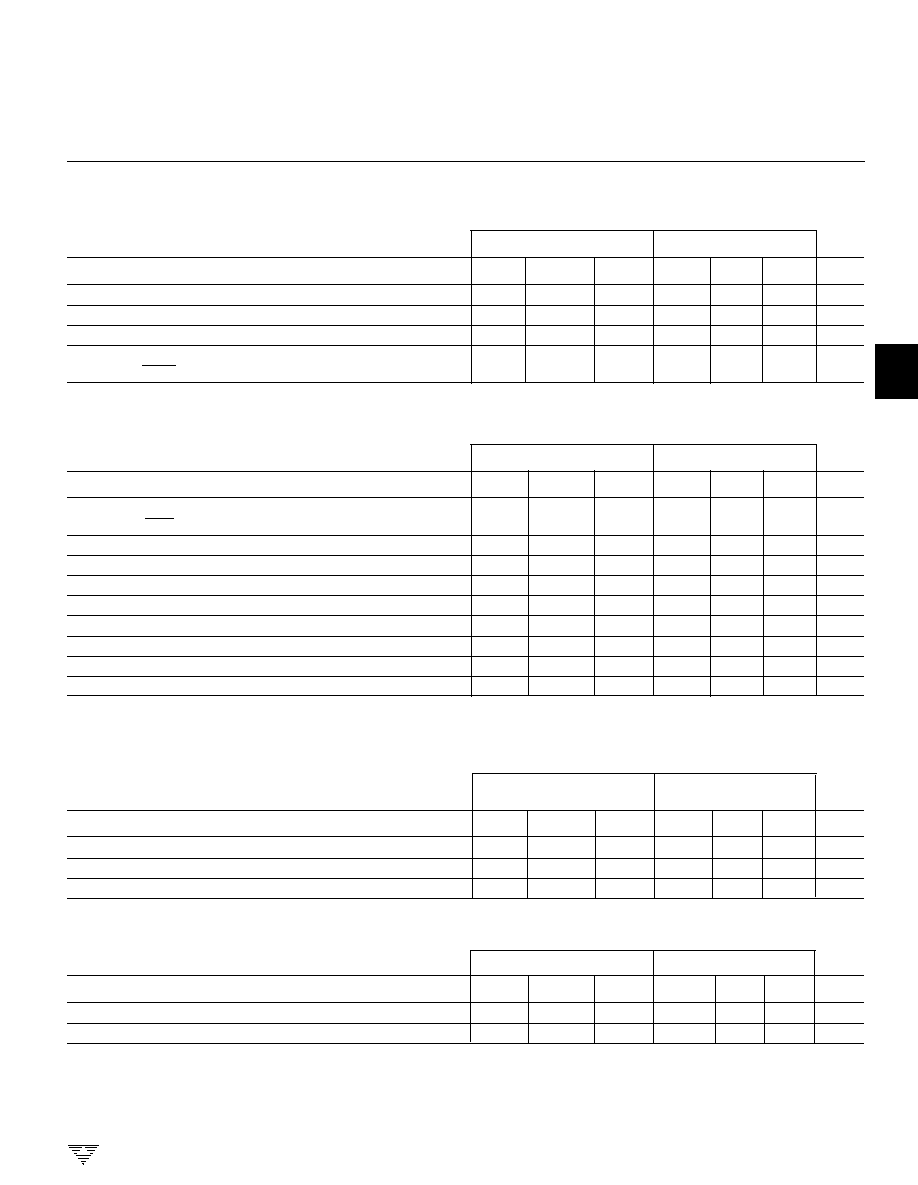
ELECTRICAL CHARACTERISTICS:
V
DD
= V
CCD
, C
AZ
= C
REF
= 0.47
�
F, unless otherwise specified.
T
A
= +25
�
C
T
A
= 0
�
C to +70
�
C
Symbol
Parameter
Test Conditions
Min
Typ
Max
Min
Typ
Max
Unit
Analog
R
Resolution
Note 1
--
--
�
17
--
--
�
17
Bits
ZSE
Zero-Scale Error
--
--
0.5
--
0.005
0.012 % F.S.
with Auto Zero Phase
ENL
End Point Linearity
Note 1 and 2
--
0.015
0.030
--
0.015
0.045 % F.S.
NL
Max Deviation from Best
Notes 1 and 2
--
0.008
0.015
--
--
--
% F.S.
Straight Line Fit
ZS
TC
Zero-Scale Temperature
--
--
--
--
1
2
�
V/
�
C
Coefficient
SYE
Roll-Over Error
Note 3
--
.012
--
--
.03
--
% F.S.
FS
TC
Full-Scale Temperature
Ext. V
REF
--
--
--
--
10
--
ppm/
�
C
Coefficient
TC = 0ppm/
�
C
I
IN
Input Current
V
IN
= 0V
--
6
--
--
--
--
pA
V
CMR
Common-Mode
V
SS
+ 1.5
--
V
DD
� 1.5 V
SS
+ 1.5
--
V
DD
� 1.5
V
Voltage Range
V
INT
Integrator Output Swing
V
SS
+ 0.9
--
V
DD
� 0.9 V
SS
+ 0.9
--
V
DD
� 0.9
V
V
IN
Analog Input Signal Range
V
SS
+ 1.5
--
V
DD
� 1.5 V
SS
+ 1.5
--
V
DD
� 1.5
V
V
REF
Voltage Reference Range
V
SS
+ 1
--
V
DD
� 1
V
DD
+ 1
--
V
DD
� 1
V
t
D
Zero Crossing Comparator
--
2.0
--
--
3.0
--
�
sec
ABSOLUTE MAXIMUM RATINGS*
Supply Voltage ........................................................... +6V
Analog Input Voltage (V
+
IN
or V
�
IN
) ....................... V
DD
to V
SS
Logic Input Voltage ................. (V
DD
+ 0.3V) to (GND � 0.3V)
Ambient Operating Temperature Range
Plastic DIP Package .............................................. (C)
0
�
C to +70
�
C
SOIC Package
(C) .............................. 0
�
C to +70
�
C
PQFP Package (C) .............................. 0
�
C to +70
�
C
Storage Temperature Range .................... � 65
�
C to +150
�
C
Lead Temperature (Soldering, 10 sec) ..................... +300
�
C
*Stresses beyond those listed under "Absolute Maximum Ratings" may
cause permanent damage to the device. These are stress ratings only, and
functional operation of the device at these or any other conditions beyond
those indicated in the operational sections of the specifications is not
implied. Exposure to absolute maximum rating conditions for extended
periods may affect device reliability.
ELECTRICAL CHARACTERISTICS
T
A
= +25
�
C
T
A
= 0
�
C to +70
�
C
Symbol
Parameter
Test Conditions
Min
Typ
Max
Min
Typ
Max
Unit
V
DD
Analog Power Supply Voltage
4.5
5.0
5.5
4.5
--
5.5
V
V
CCD
Digital Power Supply Voltage
4.5
5.0
5.5
4.5
--
5.5
V
P
D
TC530/534 Total Power
V
DD
= V
CCD
= 5V
--
--
25
--
--
--
mW
Dissipation
I
S
Supply Current (V
S
+ P
IN
)
--
1.8
2.5
--
--
3.0
mA
I
CCD
Supply Current (V
CCD
P
IN
)
f
OSC
= 1MHz
--
--
1.5
--
--
1.7
mA
5V PRECISION DATA ACQUISITION
SUBSYSTEMS
TC530
TC534
3-49
TELCOM SEMICONDUCTOR, INC.
7
6
5
4
3
1
2
8
5V PRECISION DATA ACQUISITION
SUBSYSTEMS
TC530
TC534
ELECTRICAL CHARACTERISTICS:
Serial Port Interface:
V
CCD
= +5V, unless otherwise specified.
T
A
= +25
�
C
T
A
= 0
�
C to +70
�
C
Symbol
Parameter
Test Conditions
Min
Typ
Max
Min
Typ
Max
Unit
V
IH
Input Logic HIGH Level
2.5
--
--
2.5
--
--
V
V
IL
Input Logic LOW Level
--
--
0.8
--
--
0.8
V
I
IN
Input Current (DI, DO, D
CLK
)
--
--
10
--
--
--
�
A
V
OL
Logic LOW Output Voltage
I
OUT
= 250
�
A
--
0.2
0.3
--
--
0.35
V
(EOC)
ELECTRICAL CHARACTERISTICS:
Serial Port Interface:
V
CCD
= +5V, unless otherwise specified.
T
A
= +25
�
C
T
A
= 0
�
C to +70
�
C
Symbol
Parameter
Test Conditions
Min
Typ
Max
Min
Typ
Max
Unit
tR, tF
Rise and Fall Times
C
L
= 10pF
--
--
250
--
250
--
nsec
(EOC, DI, DO)
F
XTL
Crystal Frequency
--
--
2.0
--
--
2.0
MHz
F
EXT
External Frequency on OSC
IN
--
--
4.0
--
--
4.0
MHz
t
RS
Read Setup Time
1
--
--
--
1
--
�
sec
t
RD
Read Delay Time
250
--
--
--
250
--
nsec
t
DRS
D
CLK
to D
OUT
Delay
450
--
--
--
450
--
nsec
t
PWL
D
CLK
LOW Pulse Width
150
--
--
--
150
--
nsec
t
PWH
D
CLK
HIGH Pulse Width
150
--
--
--
150
--
nsec
t
DR
Data Ready Delay
200
--
--
--
200
--
nsec
ELECTRICAL CHARACTERISTICS:
DC/DC Converter Section:
V
DD
= +5V, unless otherwise specified.
T
A
= +25
�
C T
A
= 0
�
C To +70
�
C
Symbol
Parameter
Test Conditions
Min
Typ
Max
Min
Typ
Max
Unit
R
OUT
Output Resistance
I
OUT
= 10mA
--
65
85
--
--
100
f
CLK
Oscillator Frequency
C
OSC
= 0
--
100
--
--
--
--
kHz
I
OUT
V
SS
Output Current
--
--
10
--
--
10
mA
ELECTRICAL CHARACTERISTICS:
Multiplexer:
V
DD
= +5V (Note 4), unless otherwise specified.
T
A
= +25
�
C
T
A
= 0
�
C to +70
�
C
Symbol
Parameter
Test Conditions
Min
Typ
Max
Min
Typ
Max
Unit
V
INMAX
Maximum Input Voltage
� 2.5
--
2.5
�2.5
--
2.5
V
R
DSON
Drain/Source ON Resistance
--
6
10
--
--
--
k
Notes:
1. Integrate time
66msec, Auto Zero time
66msec, V
INT
(pk) = 4V.
2. End point linearity at
�
�/
,
�
�/
,
�
�/
F.S. after full scale adjustment.
3. Roll-over error is related to capacitor used for C
INT
(See "Recommended Suppliers for C
INT
", Table 2).
4. TC534 Only.

3-50
TELCOM SEMICONDUCTOR, INC.
PIN CONFIGURATIONS
1
2
3
4
20
19
18
5
6
7
8
17
23
22
21
9
10
11
12
24
25
26
27
28
TC530CPJ
16
15
13
14
V
V
CCD
D
OUT
D
CLK
C
REF
C
INT
C
AZ
BUF
ACOM
C
REF
REF
V
REF
�
+
�
�
+
CAP
AGND
RESET
�
N/C
EOC
OSC
CAP
+
28
25
24
23
22
21
20
19
18
17
27
26
TC530COI
OSC
OUT
OSC
IN
1
2
3
4
5
6
7
8
9
10
11
12
13
14
1
33
32
31
30
29
28
27
26
25
24
23
2
3
4
5
6
7
8
9
10
11
16
15
V
IN
D
IN
R/W
+
V
IN
DGND
N/C
V
V
SS
V
SS
V
SS
C
REF
C
INT
C
AZ
BUF
ACOM
C
REF
REF
V
REF
�
+
�
�
+
OSC
OUT
V
IN
+
V
IN
DGND
N/C
V
C
REF
C
INT
C
AZ
BUF
ACOM
C
REF
REF
V
REF
�
+
�
+
OSC
OUT
OSC
OUT
DGND
DGND
V
CCD
D
OUT
D
CLK
CAP
AGND
RESET
�
NC
EOC
OSC
CAP
V
CCD
V
CCD
CAP
AGND
AGND
RESET
RESET
OSC
OSC
N/C
N/C
N/C
N/C
N/C
N/C
N/C
N/C
N/C
N/C
+
�
CAP
+
CAP
CAP
�
+
OSC
IN
D
IN
R/W
TC534CPL
1
2
3
4
5
6
7
8
9
10
11
12
13
14
15
16
17
18
19
20
40
39
38
37
36
35
34
33
32
31
30
29
28
27
26
25
24
23
22
21
TC534CKW
A1
A1
A0
A0
OSC
IN
OSC
IN
D
OUT
D
OUT
D
CLK
D
CLK
EOC
N/C
N/C
N/C
D
IN
D
IN
R/W
R/W
EOC
CH1+
CH2+
CH3+
CH3
+
CH2
+
CH1
+
CH4+
CH4�
CH3�
CH2�
CH1�
V
C
REF
ACOM
C
REF
REF
�
+
�
V
REF
+
CH4+
CH4�
CH3�
CH2�
CH1�
12
13
14
15
44
43
42
41
39
38
40
N/C
C
INT
37
36
35
34
16
17
18
19 20
21 22
BUF
C
AZ
N/C
N/C
V
DD
V
DD
V
DD
V
SS
V
DD
12
13
14 15
5V PRECISION DATA ACQUISITION
SUBSYSTEMS
TC530
TC534

3-51
TELCOM SEMICONDUCTOR, INC.
7
6
5
4
3
1
2
8
PIN DESCRIPTION
Pin No.
Pin No.
Pin No
Pin No.
(TC530
(TC530
(TC534
(TC534
28-Pin
28-Pin
40-Pin
44-Pin
PDIP, 300 Mil.) SOIC)
PDIP)
PQFP)
Symbol
Description
1
1
1
40
V
SS
Analog Output. Negative power supply converter output
and reservoir capacitor connection. This output can be
used to provide negative bias to other devices in the system.
2
2
2
41
C
INT
Analog Output. Integrator capacitor connection and integrator
output.
3
3
3
42
C
AZ
Analog Input. Auto Zero capacitor connection.
4
4
4
43
BUF
Analog Output. Integrator capacitor connection and voltage
buffer output.
5
5
5
2
ACOM
Analog Input. This pin is ground for all of the analog switches
in the A/D converter. It is grounded for most applications.
ACOM and the input common pin (V
�
IN
or Chx
�
) should be
within the common mode range, CMR.
6
6
6
3
C
�
REF
Analog Input. Reference cap negative connection.
7
7
7
4
C
+
REF
Analog Input. Reference cap positive connection.
8
8
8
5
V
�
REF
Analog Input. External voltage reference negative connection.
9
9
9
6
V
+
REF
Analog Input. External voltage reference positive connection.
Not Used
Not Used
10
7
CH4
�
Analog Input. Multiplexer channel 4 negative differential
analog input.
Not Used
Not Used
11
8
CH3
�
Analog Input. Multiplexer channel 3 negative differential
analog input.
Not Used
Not Used
12
9
CH2
�
Analog Input. Multiplexer channel 2 negative differential
analog input.
Not Used
Not Used
13
10
CH1
�
Analog Input. Multiplexer channel 1 negative differential
analog input.
Not Used
Not Used
14
11
CH4
+
Analog Input. Multiplexer channel 4 positive differential
analog input.
Not Used
Not Used
15
12
CH3
+
Analog Input. Multiplexer channel 3 positive differential
analog input.
Not Used
Not Used
16
13
CH2
+
Analog Input. Multiplexer channel 2 positive differential
analog input.
Not Used
Not Used
17
14
CH1
+
Analog Input. Multiplexer channel 1 positive differential
analog input.
10
10
Not Used
Not Used
V
�
IN
Analog Input. Negative differential analog voltage input.
11
11
Not Used
Not Used
V
+
IN
Analog Input. Positive differential analog voltage input.
12
12
18
15
DGND
Analog Input. Ground connection for serial port circuit.
Not Used
Not Used
19
16
A1
Logic Level Input. Multiplexer address MSB.
Not Used
Not Used
20
17
A0
Logic Level Input. Multiplexer address LSB.
14
14
21
18
OSC
OUT
Analog Input. Timebase for state machine. This pin connects
to one side of an AT-cut crystal having an effective series
resistance of 100
(typ) and a parallel capacitance of 20pF
If an external frequency source is used to clock the TC530/534,
this pin must be left floating.
5V PRECISION DATA ACQUISITION
SUBSYSTEMS
TC530
TC534

3-52
TELCOM SEMICONDUCTOR, INC.
5V PRECISION DATA ACQUISITION
SUBSYSTEMS
TC530
TC534
PIN DESCRIPTION (Cont.)
Pin No.
Pin No.
Pin No
Pin No.
(TC530
(TC530
(TC534
(TC534
28-Pin
28-Pin
40-Pin
44-Pin
PDIP, 300 Mil.) SOIC)
PDIP)
PQFP)
Symbol
Description
15
15
22
19
OSC
IN
Analog Input. This pin connects to the other side of the
crystal described in OSC
OUT
above. The TC530/534 may also
be clocked from an external frequency source connected to
this pin. The external frequency source must be a pulse wave
form with a minimum 30% duty cycle and rise and fall times
15nsec (Max). If an external frequency source is used, OSC
OUT
must be left floating. A maximum operating frequency of 2MHz
(crystal) or 4MHz (external clock source) is permitted.
16
16
23
20
D
OUT
Logic Level Output. Serial port data output pin. This pin is
enabled only when R/W is high.
17
17
24
21
D
CLK
Logic Input, Positive and Negative Edge Triggered. Serial port
clock. When R/W is high, serial data is clocked out of the
TC530/534A (on D
OUT
) at each HIGH-to-LOW transition of
D
CLK
. A/D initialization data (LOAD VALUE) is clocked into the
TC530/534 (on D
IN
) at each LOW-to-HIGH transition of D
CLK
. A
maximum serial port D
CLK
frequency of 3MHz is permitted.
18
18
25
22
D
IN
Logic Level Input. Serial port input pin. The A/D converter
integration time (T
INT
) and Auto Zero time (T
AZ
) values are
determined by the LOAD VALUE byte clocked into this pin.
This initialization must take place at power up, and can be
rewritten (or modified and rewritten) at any time. The LOAD
VALUE is clocked into D
IN
MSB first.
19
19
26
23
R/W
Logic Level Input. This pin must be brought low to perform a
write to the serial port (e.g. initialize the A/D converter). The
D
OUT
pin of the serial port is enabled only when this pin is high.
20
20
27
24
EOC
Open Drain Output. End-of-Conversion (EOC) is asserted
any time the TC530/534 is in the AZ phase of conversion. This
occurs when either the TC530/534 initiates a normal AZ phase,
or when RESET is pulled high. EOC is returned high when the
TC530/534 exits AZ. Since EOC is driven low immediately
following completion of a conversion cycle, it can be used as
a DATA READY processor interrupt.
21
21
30
28
RESET
Logic Level Input. It is necessary to force the TC530/534 into
the Auto Zero phase when power is initially applied. This is
accomplished by momentarily taking RESET high. Using an I/O
port line from the microprocessor, or by applying an external
system reset signal, or by connecting a 0.01
�
F capacitor from
the RESET input to V
SS
.
Conversions are performed continuously as long as RESET is
low and conversion is halted when RESET is high. RESET
may therefore be used in a complex system to momentarily
suspend conversion (for example while the address lines of an
input multiplexer are changing state). In this case, RESET
should be pulled high only when the EOC is LOW to avoid
excessively long integrator discharge times which could result in
erroneous conversion (see
Applications Section).
3-53
TELCOM SEMICONDUCTOR, INC.
7
6
5
4
3
1
2
8
5V PRECISION DATA ACQUISITION
SUBSYSTEMS
TC530
TC534
Figure 1. Serial Port Timing
t
RD
t
RS
t
DRS
t
PWL
R/W
READ TIMING
READ FORMAT
WRITE FORMAT
WRITE TIMING
WRITE DEFAULT TIMING
EOC
D
OUT
D
CLK
R/W
EOC
D
OUT
D
CLK
EOC
SGN MSB
LSB
OVR
t
LS
t
DLS
t
PWL
R/W
D
IN
D
CLK
t
LDL
t
LDS
R/W
D
IN
R/W
D
OUT
D
CLK
MSB
LSB
For Polled vs Interrupt Operation and Write Value Modified Cycle Use TC520A Data Sheet Figure 1 & 2.
PIN DESCRIPTION (Cont.)
Pin No.
Pin No.
Pin No
Pin No.
(TC530
(TC530
(TC534
(TC534
28-Pin
28-Pin
40-Pin
44-Pin
PDIP, 300 Mil.) SOIC)
PDIP)
PQFP)
Symbol
Description
22
22
32
30
V
CCD
Analog Input. Power supply connection for digital logic and
serial port. Proper power-up sequencing is critical, see the
Applications section.
23
23
34
32
OSC
Input. The negative power supply converter normally runs at
a frequency of 100kHz. This frequency can be slowed down to
reduce quiescent current by connecting an external capacitor
between this pin and V
+
S
. (See
Typical Characteristics).
25
25
37
35
V
DD
Analog Input. Power supply connection for the A/D analog
section and DC-DC converter. Proper power-up sequencing is
critical, see the
Applications section.
26
26
38
36
CAP
+
Analog Input. Storage capacitor positive connection for the
DC/DC converter.
27
27
39
37
AGND
Analog Input. Ground connection for DC/DC converter.
28
28
40
38
CAP
�
Analog Input. Storage capacitor negative connection for the
DC/DC converter.
13, 24
13, 24
28, 29, 31, 1, 25, 26, 27
NC
No connect. Do not connect any signal to these pins.
33, 35, 36
29, 31, 33,
34, 39, 44,

3-54
TELCOM SEMICONDUCTOR, INC.
30
20
10
0
0.1/T
1/T
10/T
INPUT FREQUENCY
NORMAL MODE REJECTION (dB)
T = MEASUREMENT
PERIOD
EOC
t
DR
AZ
Updated Data
Ready
Updated Data
Ready
INT
D
INT
IZ
AZ
Conversion
Phase
Data to Serial
Port Transmit
Register
Figure 3. Integrating Converter Normal Mode Rejection
Figure 2. A/D Converter Timing
DETAILED DESCRIPTION
Dual Slope Integrating Converter
The TC530/534 dual slope converter operates by inte-
grating the input signal for a fixed time period, then applying
an opposite polarity reference voltage while timing the
period (counting clocks pulses) for the integrator output to
cross 0V (deintegrating). The resulting count is read as
conversion data.
A simple mathematical expression that describes dual
slope conversion is:
(1) Integrate Voltage = Deintegrate Voltage
(2)
t
INT
0
t
DINT
0
1/R
INT
C
INT
V
IN
(t)dt = 1/R
INT
C
INT
V
REF
from which:
(3)
[
]
(t
INT
)
(V
IN
)
= (V
REF
)
(R
INT
)(C
INT
)
[
]
(t
DINT
)
(R
INT
)(C
INT
)
and therefore:
(4)
V
IN
= V
REF
[ ]
t
DINT
t
INT
where: V
REF
= Reference Voltage
t
INT
= Integrate Time
t
DINT
= Reference Voltage Deintegrate Time
Inspection of equation (4) shows dual slope converter
accuracy is unrelated to integrating resistor and capacitor
values, as long as they are stable throughout the measure-
ment cycle. This measurement technique is inherently
ratiometric (i.e., the ratio between the t
INT
and t
DINT
times is
equal to the ratio between V
IN
and V
REF
).
Another inherent benefit is noise immunity. Input noise
spikes are integrated (or averaged to zero) during the
integration period. The integrating converter has a noise
immunity with an attenuation rate of at least �20dB per
decade. Interference signals with frequencies at integral
multiples of the integration period are, for the most part,
completely removed. For this reason, the integration period
of the converter is often established to reject 50/60Hz line
noise. The ability to reject such noise is shown by the plot of
Figure 3.
In addition to the two phases required for dual slope
measurement (Integrate and Deintegrate), the TC530/534
performs two additional adjustments to minimize measure-
ment error due to system offset voltages. The resulting four
internal operations (conversion phases) performed each
measurement cycle are: Auto Zero (AZ), Integrator Output
Zero (IZ), Input Integrate (INT) and Reference Deintegrate
(D
INT
). The AZ and IZ phases compensate for system offset
errors and the INT and D
INT
phases perform the actual A/D
conversion.
5V PRECISION DATA ACQUISITION
SUBSYSTEMS
TC530
TC534

3-55
TELCOM SEMICONDUCTOR, INC.
7
6
5
4
3
1
2
8
Auto Zero Phase (AZ)
This phase compensates for errors due to buffer, inte-
grator and comparator offset voltages. During this phase, an
internal feedback loop forces a compensating error voltage
on auto zero capacitor (C
AZ
). The duration of the AZ phase
is programmable via the serial port (see also Programming
AZ and INT Phase Duration paragraph of this document).
Input Integrate Phase (INT)
In this phase, a current directly proportional to differen-
tial input voltage is sourced into integrating capacitor C
INT
.
The amount of voltage stored on C
INT
at the end of the INT
phase is directly proportional to the applied differential input
voltage. Input signal polarity (sign bit) is determined at the
end of this phase. Converter resolution and conversion
speed is a function of the duration of the INT phase, which
is programmable by the user via the serial port (see also
Programming AZ and INT Phase Duration paragraph of this
document). The shorter the integration time, the faster the
speed of conversion, but the lower the resolution. Con-
versely, the longer the integration time, the greater the
resolution, but at slower the speed of conversion.
Reference Deintegrate Phase (DINT)
This phase consists of measuring the time for the
integrator output to return (at a rate determined by the
external reference voltage) from its initial voltage to 0V. The
resulting timer data is stored in the output shift register as
converted analog data.
Integrator Output Zero Phase (IZ)
This phase guarantees the integrator output is at zero
volts when the AZ phase is entered so that only true system
offset voltages will be compensated for.
All internal converter timing is derived from the fre-
quency source at OSC
IN
and OSC
OUT
. This frequency
source must be either an externally provided clock signal, or
an external crystal. If an external clock is used, it must be
connected to the OSC
IN
pin and the OSC
OUT
pin must
remain floating. If a crystal is used, it must be connected
between OSC
IN
and OSC
OUT
and physically located as
close to the OSC
IN
and OSC
OUT
pins as possible. In either
case, the incoming clock frequency is divided by four and the
resulting clock serves as the internal TC530/534 timebase.
APPLICATIONS
Programming the TC530/534
AZ and INT Phase Duration:
These two phases have equal duration determined by
the crystal (or external) frequency and the timer initialization
byte (LOAD VALUE). Timing is selected as follows:
(1) Select Integration Time
Integration time must be picked as a multiple of the
period of the line frequency. For example, t
INT
times
of 33msec, 66msec and 132msec maximize 60Hz
line rejection.
(2) Estimate Crystal Frequency
Crystal frequencies as high as 2MHz are allowed.
Crystal frequency is estimated using:
F
IN
=
2(R)
t
INT
where: R
= Desired Converter Resolution
(in counts)
F
IN
= Input Frequency (in MHz)
INT = Integration Time (in seconds)
(3) Calculate LOAD VALUE
[LOAD VALUE]
10
= 256 �
1024
(t
INT
)(F
IN
)
F
IN
can be adjusted to a standard value during this step.
The resulting base -10 LOAD VALUE must be converted to
a hexadecimal number, then loaded into the serial port prior
to initiating A/D conversion.
D
INT
and IZ Phase Timing
The duration of the D
INT
phase is a function of the
amount of voltage stored on the integrator capacitor during
INT, and the value of V
REF
. The D
INT
phase is initiated
immediately following INT and terminated when an integra-
tor output zero-crossing is detected. In general, the maxi-
mum number of counts chosen for D
INT
is twice that of INT
(with V
REF
chosen at V
IN
(max)/2).
System RESET
The TC530/534 must be forced into the AZ state when
power is first applied. A .01
�
F capacitor connected from
RESET to V
CC
(or external system reset logic signal) can be
used to momentarily drive RESET high for a minimum of
100msec.
Selecting Component Values for the TC530/534
(1) Calculate Integrating Resistor (R
INT
)
The desired full-scale input voltage and amplifier
output current capability determine the value of R
INT
.
The buffer and integrator amplifiers each have a full-
scale current of 20
�
A.
The value of R
INT
is therefore directly calculated as
follows:
5V PRECISION DATA ACQUISITION
SUBSYSTEMS
TC530
TC534

3-56
TELCOM SEMICONDUCTOR, INC.
5V PRECISION DATA ACQUISITION
SUBSYSTEMS
TC530
TC534
20
V
INMAX
R
INT
(M
) =
where: V
INMAX
= Maximum Input Voltage (full count
voltage)
R
INT
= Integrating Resistor (in M
)
For loop stability, R
INT
should be
50k
.
(2) Select Reference (C
REF
) and Auto Zero (C
AZ
)
Capacitors
C
REF
and C
AZ
must be low leakage capacitors (such
as polypropylene). The slower the conversion rate,
the larger the value C
REF
must be. Recommended
capacitors for C
REF
and C
AZ
are shown in Table 1.
Larger values for C
AZ
and C
REF
may also be used to
limit roll-over errors.
Table 1. C
REF
and C
AZ
Selection
Conversions Typical Value of Suggested *
Per Second
C
REF
, C
AZ
(
�
F)
Part Number
>7
0.1
WIMA MK12 .1/63/20
2 to 7
0.22
WIMA MK12 .22/63/20
2 or less
0.47
WIMA MK12 .47/63/20
*WIMA Corp. listing on the last page of this data sheet.
3. Calculate Integrating Capacitor (C
INT
)
The integrating capacitor must be selected to maxi-
mize integrator output voltage swing. The integrator
output voltage swing is defined as the absolute value
of V
DD
(or V
SS
) less 0.9V (i.e. |V
DD
� 0.9V| or |V
SS
+
0.9V|). Using the 20
�
A buffer maximum output
current, the value of the integrating capacitor is
calculated using the following equation:
(V
S
� 0.9)
(t
INT
)(20)
C
INT
(
�
F) =
where: t
INT
= Integration Period
V
S
= Applied Supply Voltage
C
INT
= Integrator Capacitor Value (in
�
F)
It is critical that the integrating capacitor have a very
low dielectric absorption. PPS capacitors are an
example of one such chemistry. Table 2 summa-
rizes various capacitors suitable for C
INT
.
Value
Suggested Part Number*
0.1
WIMA MK12 .1/63/20
0.22
WIMA MK12 .22/63/20
0.33
WIMA MK12 .33/63/20
0.47
WIMA MK12 .47/63/20
*WIMA Corp. listing on the last page of this data sheet.
4. Calculate V
REF
The reference deintegration voltage is calculated
using:
V
REF
(in Volts) =
(V
S
� 0.9)(C
INT
)(R
INT
)
2(t
INT
)
Serial Port
Communication with the TC530/534 is accomplished
over a 3 wire serial port. Data is clocked into D
IN
on the rising
edge of D
CLK
and clocked out of D
OUT
on the falling edge of
D
CLK
. R/W must be HIGH to read converted data from the
serial port and LOW to write the LOAD VALUE to the TC530/
534.
Load Value Write Cycle (Figure 4)
Following the power-up reset pulse, the LOAD VALUE
(which sets the duration of AZ and INT) must next be
transmitted to the serial port. To accomplish this, the proces-
sor monitors the state of EOC (which is available as a
hardware output or at D
OUT
). R/W is taken low to initiate the
write cycle only when EOC is low (during the AZ phase).
(Failure to observe EOC low may cause an offset voltage to
be developed across C
INT
resulting in erroneous readings).
The 8 bit LOAD VALUE data on D
IN
is clocked in by D
CLK
.
The processor then terminates the write cycle by taking
R/W high. (Data is transferred from the serial input shift
register to the time base counter on the rising edge of R/W,
and data conversion is initiated).
Data Read Cycle (Figure 5)
Data is shifted out of the serial port in the following order:
End of Conversion (EOC), Overrange (OVR), Sign (SGN),
conversion data (MSB first). When R/W is high, the state of
the EOC bit can be polled by simply reading the state of
D
OUT
. This allows the processor to determine if new data is
available without connecting an additional wire to the EOC
output pin (this is especially useful in a polled environment).
Input Multiplexer (TC534 Only)
A 4 input, differential multiplexer is included in the
TC534. The states of channel address lines A0 and A1
determine which differential V
IN
pair is routed to the con-
Table 2. Recommend Capacitor for C
INT
3-57
TELCOM SEMICONDUCTOR, INC.
7
6
5
4
3
1
2
8
5V PRECISION DATA ACQUISITION
SUBSYSTEMS
TC530
TC534
verter input. A0 is the least significant address bit (i.e.,
channel 1 is selected when A0 = 1 and A1 = 0). The
multiplexer is designed to be operated in a differential mode.
For single-ended inputs, the CHx
�
input for the channel
under selection must be connected to the ground reference
associated with the input signal.
EOC
R/W
RESET
D
CLK
D
IN
1
1
0
0
1
1
1
1
AZ
AZ
LOAD VALUE
MSB
LSB
INT
DINT
IZ
AZ...
Conversion
Phase
Timing
Status
Converter held in AZ
state due to RESET = 1
Write LOAD VALUE to Serial Port
Power-up RESET
Undefined
Converter in Normal Service
R/W brought LOW during AZ
for serial port write cycle
R/W = HIGH strobes
LOAD VALUE into
timebase and starts
conversion
Continuous Conversions
Figure 4. TC530/534 Initialization and Load Value Write Cycle
EOC
OVR POL MSB
LSB
R/W
D
CLK
D
OUT
Figure 5. Serial Port Data Read Cycle
DC/DC Converter
An on-board, TC7660H-type charge pump supplies
negative bias to the converter circuitry, as well as to external
devices. The charge pump develops a negative output
voltage by moving charge from the power supply to the
reservoir capacitor at V
SS
by way of the commutating
capacitor connected to the CAP
+
and CAP
�
inputs.
The charge pump clock operates at a typical frequency
of 100kHz. If lower quiescent current is desired, the charge
pump clock can be slowed by connecting an external ca-
pacitor from the OSC pin to V
DD
. Reference typical charac-
teristics curves.
APPLICATIONS
Design Example
Figure 6 shows a typical TC534 interrupt-driven applica-
tion. Timing and component values are calculated from
equations and recommendations made in the Dual Slope
Integrating Converter and Programming the TC530/534
sections of this document. The EOC connection to the
processor INT input is for interrupt-driven applications only.
(In polled systems, the EOC output is available on D
OUT
).
GIVEN
REQUIRED RESOLUTION:
16 Bits (65,536 counts.)
MAXIMUM V
IN
:
�
2V
POWER SUPPLY VOLTAGE: +5V
60Hz SYSTEM
1. Pick Integration time (t
INT
)
66msec
2. Estimate crystal frequency
F
IN
= 2R/t
INT
= 2 x 65536/66 x 10
�3
= 1.98MHz
(use 2MHz)
3-58
TELCOM SEMICONDUCTOR, INC.
5V PRECISION DATA ACQUISITION
SUBSYSTEMS
TC530
TC534
Figure 6. TC530/534 Typical Application
A0
A1
RESET
EOC
VCCD
VCCD
VDD
VDD
D
OUT
D
CLK
X1: 2MHz
R2
100k
R1
100k
100
1
�
F
TC04
(1.25V V
REF
)
(1.03V)
D
IN
R/W
ACOM
OSC
IN
OSC
OUT
V
SS
DGND
C
AZ
C
AZ
0.22
�
F
C
IN
0.33
�
F
R
I
NT
100k
TC534
C
INT
Analog
Inputs
Channel
Control
C1
.01
�
F
10
�
F
MUX
IN1
+
IN1
�
IN2
+
IN2
�
IN3
+
IN3
�
IN4
+
IN4
�
+5V
+5V
�5V
(Optional)
BUF
V
REF
+
V
REF
�
+
C
REF
C
REF
�
C
REF
0.22
�
F
+
CAP
CAP
�
1
�
F
+5V
INT
PROCESSOR
I/O
I/O
I/O
I/O
.01
�
F
.01
�
F
1
�
F
3. Calculate LOAD VALUE
LOAD VALUE = 256 � (t
INT
)(F
IN
)/1024 = [128]
10
[128]
10
= 80 hex
4. Calculate R
INT
R
INT
(in M
) = V
INMAX
/20 = 2/20 = 100k
5. Calculate C
INT
for maximum (4V) integrator out-
put swing
C
INT
(in
�
F) = (t
INT
)(20 x 10
�6
)/ (V
S
� 0.9)
= (.066)(20 x 10
�6
)/(4.1)
= .32
�
F (use closest value: 0.33
�
F)
NOTE: TelCom recommended capacitor:
WIMA p/n: MK12 .33/63/10
6. Choose C
REF
and C
AZ
based on conversion rate
Conversions/sec = 1/(t
AZ
+ t
INT
+ 2t
INT
+ 2msec)
= 1/(66msec + 66msec + 132msec
+ 2msec)
= 3.7 conversions/sec
from which C
AZ
= C
REF
= 0.22
�
F (see Table 1)
NOTE: TelCom recommended capacitor:
WIMA p/n: MK12 .22/63/10
7. Calculate V
REF
V
REF
(in Volts = (V
S
� 0.9)(C
INT
)(R
INT
)
2(t
INT
)
= (4.1)(0.33x10
�6
)(10
5
)/2(.066)
= 1.025V
Power Supply Sequencing
Improper sequencing of the power supply inputs (V
DD
vs. V
CCD
) can potentially cause an improper power-up
sequence to occur. See
Circuit Design/Layout Consider-
ations below. Failing to insure a proper power-up sequence
can cause spurious operation.
Ciruit Design/Layout Considerations
(1) Separate ground return paths should be used for the
analog and digital circuitry. Use of ground planes and trace
fill on analog circuit sections is highly recommended
EXCEPT for in and around the integrator section and
C
REF
, C
AZ
. (C
INT
, C
REF
, C
AZ
, R
INT
). Stray capacitance be-
tween these nodes and ground appears in parallel with the
components themselves and can affect measurement accu-
racy.

3-59
TELCOM SEMICONDUCTOR, INC.
7
6
5
4
3
1
2
8
5V PRECISION DATA ACQUISITION
SUBSYSTEMS
TC530
TC534
TC530EV Evaluation Kit
The TC530EV consists of a 4" x 6" pre-assembled circuit
board that connects to the serial port of any PC or dumb
terminal. Also included is a Windows
TM*
Excel
TM*
-based
design utility that calculates component and LOAD values
based on user input, and prints a finished circuit schematic.
Please contact your local TelCom representative for more
information, or point your web browser to http://www.telcom-
semi.com.
(2) Improper sequencing of the power supply inputs
(V
DD
vs. V
CCD
) can potentially cause an improper power-up
sequence to occur in the internal state machines. It is
recommended that the digital supply, V
CCD
, be powered up
first. One method of insuring the correct power-up sequence
is to delay the analog supply using a series resistor and a
capacitor. See Figure 6, TC530/534 Typical Application.
(3) Decoupling capacitors, preferably a higher value elec-
trolytic or tantulum in parallel with a small ceramic or
tantalum, should be used liberally. This includes bypassing
the supply connections of all active components and the
voltage reference.
(4) Critical components should be chosen for stability and
low noise. The use of a metal-film resistor for R
INT
and
Polypropylene or Polyphenelyne Sulfide (PPS) capacitors
for C
INT
, C
AZ
, and C
REF
is highly recommended.
(5) The inputs and integrator section are very high imped-
ance nodes. Leakage to or from these critical nodes can
contribute measurement error. A guard-ring should be used
to protect the integrator section from stray leakage.
(6) Circuit assemblies should be scrupulously clean to
prevent the presence of contamination from assembly,
handling, or the cleaning itself. Minutely conductive trace
contaminates, easily ignored in most applications, can ad-
versely affect the performance of high impedance circuits.
The input and integrator sections should be made as com-
pact and close to the TC53x as possible.
(7) Digital and other dynamic signal conductors should be
kept as far from the TC53x's analog section as possible. The
microcontroller or other host logic should be kept quiet
during a measurement cycle. Background activites such as
keypad scanning, display refreshing, and power switching
can introduce noise.
*All trademarks are the property of their respective owners.
3-60
TELCOM SEMICONDUCTOR, INC.
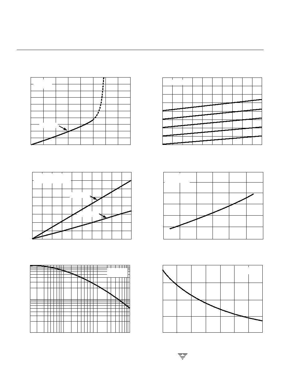
TYPICAL CHARACTERISTICS
LOAD CURRENT (mA)
OUTPUT CURRENT (mA)
�5
�4
�3
�2
�1
0
1
2
3
4
5
0
10
20
30
40
50
60
70
0
6
8
10
4
2
14
16
18
12
20
80
OUTPUT VOLTAGE (V)
Output Voltage vs Load Current
�0
�1
�3
�2
�4
�5
�7
�6
�8
OUTPUT VOLTAGE (V)
Output Voltage vs. Output Current
OSCILLATOR CAPACITANCE (pF)
100
10
1
1
10
100
1000
OSCILLATOR FREQUENCY (kHz)
Oscillator Frequency vs. Capacitance
LOAD CURRENT (mA)
0
3
4
5
6
1
2
7
8
9
10
0
25
50
75
100
125
150
175
200
OUTPUT RIPPLE (mV PK-PK)
Output Ripple vs. Load Current
TEMPERATURE (
�
C)
70
80
90
100
60
50
40
�50
0
25
�25
50
75
100
OUTPUT SOURCE RESISTANCE (
)
Output Source Resistance vs. Temperature
T
A
= 25
�
C
V+ = 5V
T
A
= +25
�
C
V+ = 5V
T
A
= 25
�
C
Slope 60
V+ = 5V, T
A
= 25
�
C
Osc. Freq. = 100kHz
CAP = 1
�
F
CAP = 10
�
F
V+ = 5V
I
OUT
= 10mA
TEMPERATURE (
�
C)
125
150
100
75
50
�50
0
25
�25
50
75
125
100
OSCILLATOR FREQUENCY (kHz)
Oscillator Frequency vs. Temperature
V+ = 5V
5V PRECISION DATA ACQUISITION
SUBSYSTEMS
TC530
TC534

3-61
TELCOM SEMICONDUCTOR, INC.
7
6
5
4
3
1
2
8
WIMA Corporation Capacitor Representatives (Tables 1 and 2)
Malaysia:
MA ELECTRONICS (M) SDN BHD
346-B Jalan Jelutong
11600 Penang
Tel.: 6 04-2 81 45 18
Fax: 6 04-2 81 45 15
Singapore:
MICROTRONICS ASSOC. (PTE.) LTD.
8, Lorong Bakar Batu
03-01, Kolam Ayer Ind. Park
Singapore 1334
Tel.: 65-7 48-18 35
Tlx: 34 929
Fax: 65-7 43-30 65
South Africa:
KOPP ELECTRONICS LIMITED
P.O. Box 3853
2128 Rivonia
Tel.: 0 11-4 44-23 33
Fax: 0 11-4 44-17 06
South Korea:
YONG JUN ELECTRONIC CO.
#201, Sungwook Bldg.
1460-16, Seocho-Dong
Seocho-Ku
Seoul, Korea
Tel.: 2-52 31 80 02
Fax: 2-5 23 18 03
Taiwan, R.O.C.:
SOLOMON TECHNOLOGY CORP.
7th Floor No. 2
Lane 47, Sec. 3
Nan Kang Road
Taipei
Tel.: 8 86-2-7 88 89 89
Fax: 8 86-2-7 88 82 75
Thailand:
MICROTRONICS THAI LTD.
50/68 T.T. Court
Cheng Wattana Road
Amphur Pak-Kreed
Nonthaburi 11120
Tel.: 6 62-5 84 58 07, Ext. 102
Fax: 6 62-5 83 37 75
USA:
THE INTER-TECHNICAL GROUP, INC.
WIMA DIVISION
175 Clearbrook Road
P.O. Box 535
Elmsford, NY 10523-0535
Tel.: 914-347-2474
Fax: 914-347-7230
TAW ELECTRONICS, INC.
4215, W. Burbank, Blvd.
Burbank, CA, 91505
Tel.: 8 18-8 46-39 11
Fax: 8 18-8 46-11 94
Venezuela:
MAGNETICA, S.A.
Apartado 78117
Caracas 1074 A
Tel.: 58-2-2 41 75 09
Fax: 58-2-2 41 55 42
Australia:
ADILAM ELECTRONICS (PTY.) LTD.
P.O. Box 664
3 Nicole Close
Bayswater 3153
Tel.: 3-7 61 44 66
Fax: 3-7 61 41 61
Canada:
R-THETA INC.
130 Matheson Blvd. East, Unit 2
Mississauga, Ont. L4Z1Y6
Tel.: 9 05-8 90-02 21
Fax: 9 05-8 90-16 28
Hong Kong:
REALTRONICS CO. LTD.
E-3, Hung-On Building
2, King's Road
Tel.: 25 70 11 51
Fax: 28 06 84 74
India:
SUSAN AGENCIES
P.O. Box 2138
Srirampuram P.O.
Bangalore-560 021
Tel.: 0 80-3 32 06 62
Fax: 0 80-3 32 43 38
Israel:
M.G.R. TECHNOLOGY
P.O. Box 2229
Rehavot 76121
Tel.: 9 72-8-41 17 19
Fax: 9 72-8-41 41 78
Japan:
UNIDUX INC.
5-1-21, Kyonan-Cho
Musashino-Shi
Tokyo 180
Tel.: 04 22-32-41 11
Fax: 04 22-32-03 31
5V PRECISION DATA ACQUISITION
SUBSYSTEMS
TC530
TC534