 | –≠–ª–µ–∫—Ç—Ä–æ–Ω–Ω—ã–π –∫–æ–º–ø–æ–Ω–µ–Ω—Ç: TC7117A | –°–∫–∞—á–∞—Ç—å:  PDF PDF  ZIP ZIP |
Document Outline
- Return to Contents
- List of Figures
- 1. Typical TC7116/A/7/A Operating Circuit
- 3. Analog Section of TC7116/TC7116A and TC7117/TC7117A
- 4. Using an External Reference
- 5. Simple Inverter for Fixed Decimal Point
- 6. Exclusive çORé Gate for Decimal Point Drive
- 7. Clock Circuits
- 8. TC7116/TC7116A Digital Section
- 9. TC7117/TC7117A Digital Section
- 10. Negative Power Supply Generation With TC7660
- 11. TC7116/TC7116A Using the Internal Reference
- 12. TC7117/TC7117A Internal Reference (200 mV Full Scale,
- 13. Circuit for Developing Underrange and Overrange
- 14. TC7117/TC7117A With a 1.2V External Band-Gap
- 15. Recommended Component Values for 2V Full Scale
- 16. TC7117/TC7117A Operated from Single +5V Supply
- 17. TC7117/TC7117A Output Current vs Output Voltage
- 18. Diode or Resistor Limits Package Power Dissipation
- Features
- Ordering Information
- General Description
- Absolute Maximum Ratings*
- Electrical Characteristics
- Electrical Characteristics (Cont.)
- Pin Configurations
- Pin Description
- Pin Description (Cont.)
- Analog Section
- Auto-Zero Phase
- Signal-Integrate Phase
- Reference Integrate Phase
- Reference
- Differential Input
- Analog Common
- Test
- Digital Section
- System Timing
- HOLD Reading Input
- Component Value Selection
- Auto-Zero Capacitor
- Reference Capacitor
- Integrating Capacitor
- Integrating Resistor
- Oscillator Components
- Reference Voltage
- TC7117/TC7117A Power Supplies
- Typical Applications
- Applications Information

3-203
TELCOM SEMICONDUCTOR, INC.
7
6
5
4
3
1
2
8
3-1/2 DIGIT ANALOG-TO-DIGITAL CONVERTERS WITH HOLD
VREF
+
TC7116/A
9V
VREF
33
34
24 k
1 k
31
29
36
39
38
40
0.47 µF
0.1 µF
V
≠
1
OSC
3
OSC
2
OSC
TO ANALOG
COMMON (PIN 32)
3 CONVERSIONS/SEC
COSC
100 k
47 k
0.22 µF
0.01 µF
ANALOG
INPUT
+
≠
CREF
≠
CREF
+
VIN
+
VIN
≠
ANALOG
COMMON
VINT
VBUFF
CAZ
20
21
35
SEGMENT
DRIVE
2≠19
22≠25
POL
BP/GND
V
+
MINUS SIGN
BACKPLANE
DRIVE
28
ROSC 100 pF
LCD DISPLAY (TC7116/7116A)
OR COMMON ANODE LED
DISPLAY (TC7117/7117A)
1 M
27
30
32
HLDR
DISPLAY
HOLD
100 mV
1
26
TC7117/A
+
FEATURES
s
Low Temperature Drift Internal Reference
TC7116/TC7117 ............................. 80 ppm/
∞
C Typ
TC7116A/TC7117A ........................ 20 ppm/
∞
C Typ
s
Display Hold Function
s
Directly Drives LCD or LED Display
s
Guaranteed Zero Reading With Zero Input
s
Low Noise for Stable
Display ......... 2V or 200 mV Full-Scale Range (FSR)
s
Auto-Zero Cycle Eliminates Need for Zero
Adjustment Potentiometer
s
True Polarity Indication for Precision Null
Applications
s
Convenient 9V Battery Operation
(TC7116/TC7116A)
s
High Impedance CMOS Differential Inputs .... 10
12
s
Low Power Operation .................................... 10 mW
GENERAL DESCRIPTION
The TC7116A/TC7117A are 3-1/2 digit CMOS analog-
to-digital converters (ADCs) containing all the active
components necessary to construct a 0.05% resolution
measurement system. Seven-segment decoders, polarity
and digit drivers, voltage reference, and clock circuit are
integrated on-chip. The TC7116A drives liquid crystal
displays (LCDs) and includes a backplane driver. The
TC7117A drives common anode light emitting diode (LED)
displays directly with an 8-mA drive current per segment.
These devices incorporate a display hold (HLDR)
function. The displayed reading remains indefinitely, as
long as HLDR is held high. Conversions continue, but
output data display latches are not updated. The reference
low input (V
≠
REF
) is not available as it is with the TC7106/
7107. V
≠
REF
is tied internally to analog common in the
TC7116A/7117A devices.
The TC7116A/7117A reduces linearity error to less
than 1 count. Roll-over error (the difference in readings for
equal magnitude but opposite polarity input signals) is
below
±
1 count. High-impedance differential inputs offer 1
pA leakage current and a 10
12
input impedance. The 15
µ
V
P-P
noise performance guarantees a "rock solid" reading.
The auto-zero cycle guarantees a zero display reading with
a 0V input.
The TC7116A and TC7117A feature a precision, low-
drift internal reference, and are functionally identical to the
TC7116/TC7117. A low-drift external reference is not
normally required with the TC7116A/TC7117A.
AVAILABLE PACKAGES
40-Pin Plastic
DIP
40-Pin CerDIP
44-Pin Plastic Quad Flat
Package Formed Leads
44-Pin Plastic Chip
Carrier PLCC
Package
Temperature
Code
Package
Range
CKW
44-Pin PQFP
0
∞
C to +70
∞
C
CLW
44-Pin PLCC
0
∞
C to +70
∞
C
CPL
40-Pin Plastic DIP
0
∞
C to +70
∞
C
IJL
40-Pin CerDIP
≠ 25
∞
C to +85
∞
C
Figure 1. Typical TC7116/A/7/A Operating Circuit
TC7116
TC7116A
TC7117
TC7117A
TC7116/A/7117/A-7 10/18/96
ORDERING INFORMATION
PART CODE
TC711X X X XXX
6 = LCD
7 = LED
A or blank*
R (reversed pins) or blank (CPL pkg. only)
* "A" parts have an improved reference TC
Package Code (see below):
}

3-204
TELCOM SEMICONDUCTOR, INC.
3-1/2 DIGIT ANALOG-TO-DIGITAL
CONVERTERS WITH HOLD
TC7116
TC7116A
TC7117
TC7117A
ABSOLUTE MAXIMUM RATINGS*
Supply Voltage
TC7116/TC7116A: V
+
to V
≠
................................. 15V
TC7117/TC7117A: V
+
to GND ............................. +6V
V
≠
to GND ............................ ≠ 9V
Analog Input Voltage (Either Input) (Note 1) ........ V
+
to V
≠
Reference Input Voltage (Either Input) ................. V
+
to V
≠
Clock Input
TC7116/TC7116A ..................................... TEST to V
+
TC7117/TC7117A ...................................... GND to V
+
Package Power Dissipation, T
A
70
∞
C (Note 2)
CerDIP .............................................................. 2.29W
Plastic DIP ........................................................ 1.23W
Plastic Chip Carrier (PLCC) .............................. 1.23W
Plastic Quad Flat Package (PQFP) .................. 1.00W
Operating Temperature
"C" Device .............................................. 0
∞
C to +70
∞
C
"I" Device .......................................... ≠ 25
∞
C to +85
∞
C
Storage Temperature ............................ ≠ 65
∞
C to +150
∞
C
Lead Temperature (Soldering, 10 sec) ................. +300
∞
C
*Static-sensitive device. Unused devices must be stored in conductive
material. Protect devices from static discharge and static fields. Stresses
above those listed under Absolute Maximum Ratings may cause perma-
nent damage to the device. These are stress ratings only and functional
operation of the device at these or any other conditions above those
indicated in the operational sections of the specifications is not implied.
Exposure to Absolute Maximum Rating Conditions for extended periods
may affect device reliability.
ELECTRICAL CHARACTERISTICS
(Note 3)
Parameter
Test Conditions
Min
Typ
Max
Unit
Zero Input Reading
V
IN
= 0V
--
±
0
--
Digital
Full Scale = 200 mV
Reading
Ratiometric Reading
V
IN
= V
REF
999
999/1000
1000
Digital
V
REF
= 100 mV
Reading
Roll-Over Error (Difference in
≠V
IN
= +V
IN
200 mV or
2V
≠ 1
±
0.2
+1
Counts
Reading for Equal Positive and
Negative Readings Near Full Scale)
Linearity (Maximum Deviation From
Full Scale = 200 mV or 2V
≠ 1
±
0.2
+1
Counts
Best Straight Line Fit)
Common-Mode Rejection Ratio (Note 4)
V
CM
=
±
1V, V
IN
= 0V
--
50
--
µ
V/V
Full Scale = 200 mV
Noise (Peak-to-Peak Value Not
V
IN
= 0V
--
15
--
µ
V
Exceeded 95% of Time)
Full Scale = 200 mV
Leakage Current at Input
V
IN
= 0V
--
1
10
pA
Zero Reading Drift
V
IN
= 0V
"C" Device: 0
∞
C to +70
∞
C
--
0.2
1
µ
V/
∞
C
"I" Device: ≠25
∞
C to +85
∞
C
--
1
2
µ
v/
∞
C
Scale Factor Temperature Coefficient
V
IN
= 199 mV
"C" Device: 0
∞
C to +70
∞
C
--
1
5
ppm/
∞
C
(Ext Ref = 0 ppm/
∞
C)
"I" Device: ≠25
∞
C to +85
∞
C
--
--
20
ppm/
∞
C
Input Resistance, Pin 1
Note 6
30
70
--
k
V
IL
, Pin 1
TC7116/A Only
--
--
Test +1.5
V
V
IL
, Pin 1
TC7117/A Only
--
--
GND +1.5
V
V
IH
, Pin 1
Both
V
+
≠ 1.5
--
--
V
Supply Current (Does Not Include
V
IN
= 0V
--
0.8
1.8
mA
LED Current for 7117/A)
Analog Common Voltage
25 k
Between Common
2.4
3.05
3.35
V
(With Respect to Positive Supply)
and Positive Supply
Temperature Coefficient of Analog Common
"C" Device: 0
∞
C to +70
∞
C
(With Respect to Positive Supply)
TC7116A/TC7117A
--
20
50
ppm/
∞
C
TC7116/TC7117
--
80
--
ppm/
∞
C

3-205
TELCOM SEMICONDUCTOR, INC.
7
6
5
4
3
1
2
8
3-1/2 DIGIT ANALOG-TO-DIGITAL
CONVERTERS WITH HOLD
TC7116
TC7116A
TC7117
TC7117A
ELECTRICAL CHARACTERISTICS (Cont.)
Parameter
Test Conditions
Min
Typ
Max
Unit
Temperature Coefficient of Analog Common
"I" Device: ≠25
∞
C to +85
∞
C
--
--
75
ppm/
∞
C
(With Respect to Positive Supply)
25 k
Between Common and
Positive Supply (TC7116A/TC7117A)
TC7116/TC7116A ONLY Peak-to-Peak
V
+
to V
≠
= 9V
4
5
6
V
Segment Drive Voltage
(Note 5)
TC7116/TC7116A ONLY Peak-to-Peak
V
+
to V
≠
= 9V
4
5
6
V
Backplane Drive Voltage
(Note 5)
TC7117/TC7117A ONLY Segment
V
+
= 5V
5
8
--
mA
Sinking Current (Except Pin 19)
Segment Voltage = 3V
TC7117/TC7117A ONLY Segment
V
+
= 5V
10
16
--
mA
Sinking Current (Pin 19 Only)
Segment Voltage = 3V
NOTES: 1. Input voltages may exceed supply voltages, provided input current is limited to
±
100
µ
A.
2. Dissipation rating assumes device is mounted with all leads soldered to printed circuit board.
3. Unless otherwise noted, specifications apply at T
A
= +25
∞
C, f
CLOCK
= 48 kHz. TC7116/TC7116A and TC7117/TC7117A are tested in the
circuit of Figure 1.
4. Refer to "Differential Input" discussion.
5. Backplane drive is in-phase with segment drive for "OFF" segment, 180
∞
out-of-phase for "ON" segment. Frequency is 20 times
conversion rate. Average DC component is less than 50 mV.
6. The TC7116/TC7116A logic inputs have an internal pull-down resistor connected from HLDR, pin 1 to TEST, pin 37.
The TC7117/TC7117A logic inputs have an internal pull-down resistor connected from HLDR, pin 1 to GND, pin 21.
3-206
TELCOM SEMICONDUCTOR, INC.
TC7116
TC7116A
TC7117
TC7117A
BP/
GND
33
34
35
36
37
38
39
13
10
9
8
7
COMMON
V
+
18
19
20
21
23
24
3
AB
4
POL
NC
IN HI
NC
IN LO
B
6
5
4
3
1
44
2
A
OSC
22
43
OSC
42
OSC
41
TEST
40
REF HI
25
26
27
28
F
E
G
A
C
G
32
14
A/Z
2
31
15
BUFF
2
30
16
INT
E
29
17
D
NC
11
12
NC
C
D
3
2
F
A
2
2
2
B
3
3
3
3
3
2
TC7116CLW
TC7116ACLW
TC7117CLW
TC7117ACLW
(PLCC)
1
2
3
V
≠
CREF
CREF
1
B
1
C
1
D
1
F1
G1
E1
BP/
GND
27
28
29
30
31
32
33
7
4
3
2
1
NC
TC7116CKW
TC7116ACKW
TC7117CKW
TC7117ACKW
12
13
14
15
17
18
G
44
43
42
41
39
38
40
REF HI
COMMON
16
37
A/Z
36
BUFF
35
INT
34
V
19
20
21
22
D
26
8
25
9
24
10
23
11
IN HI
5
6
C
OSC
TEST
NC
NC
HLDR
3
3
D
2
C
2
B
2
A
2
F
2
E
2
NC
OSC2
OSC1
V
+
REF
C
REF
C
IN LO
≠
2
3
A3
G3
POL
AB4
E3
F3
B3
(FLAT PACKAGE)
D1
C1
B1
A
1
F
1
G
1
E
1
TC7116IPL
TC7116AIPL
TC7117CPL
TC7117ACPL
(PDIP)
1
2
3
4
OSC 1
5
6
7
8
9
10
11
12
TEST
V
COMMON
CAZ
HLDR
D
13
14
15
16
17
18
19
20
40
39
38
37
36
35
34
33
32
31
30
29
28
27
26
25
24
23
22
21
2
C2
B2
A2
F2
E2
D3
B3
F3
E3
AB4
(MINUS SIGN)
10's
100's
1000's
(TC7116/7117)
(TC7116A/TC7117A)
100's
OSC2
OSC 3
+
REF
V+
C
+
REF
C
≠
REF
V
+
IN
V
≠
IN
VBUFF
VINT
V ≠
G
C
A
G
BP/GND
POL
3
3
3
2
D1
C1
B1
A1
F1
G1
E1
1's
NOTES:
1. NC = No internal connection.
2. Pins 9, 25, 40, and 56 are connected to the die substrate. The potential at these pins is approximately V . No external connections
should be made.
+
+
≠
+
≠
HLDR
TC7116IJL
TC7116AIJL
TC7117IJL
TC7117AIJL
(CerDIP)
1
2
3
4
OSC 1
5
6
7
8
9
10
11
12
TEST
V
COMMON
CAZ
HLDR
D
13
14
15
16
17
18
19
20
40
39
38
37
36
35
34
33
32
31
30
29
28
27
26
25
24
23
22
21
2
C2
B2
A2
F2
E2
D3
B3
F3
E3
AB4
(MINUS SIGN)
10's
100's
1000's
(TC7116/7117)
(TC7116A/TC7117A)
100's
OSC2
OSC 3
+
REF
V+
C
+
REF
C
≠
REF
V
+
IN
V
≠
IN
VBUFF
VINT
V ≠
G
C
A
G
BP/GND
POL
3
3
3
2
D1
C1
B1
A1
F1
G1
E1
1's
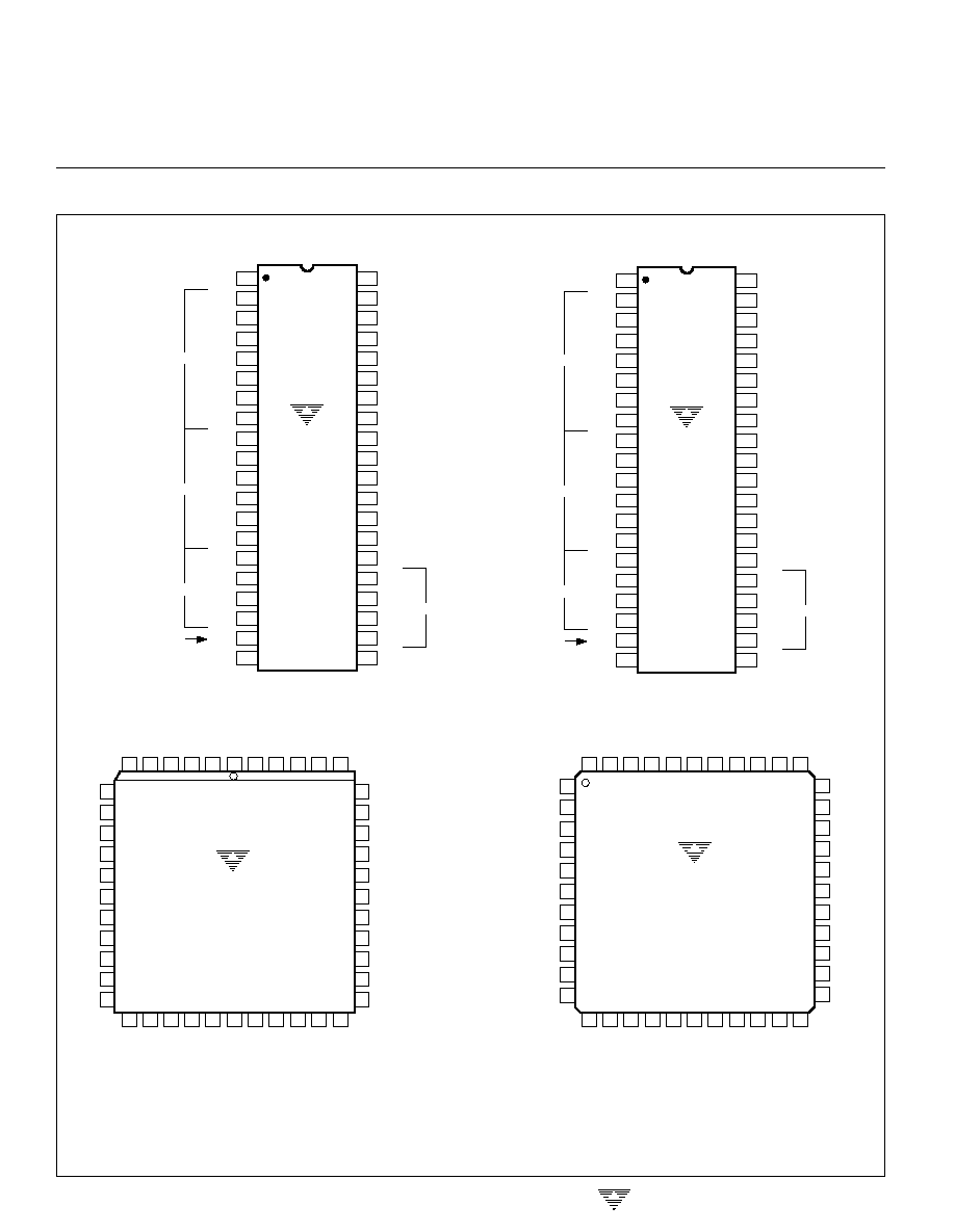
PIN CONFIGURATIONS
3-1/2 DIGIT ANALOG-TO-DIGITAL
CONVERTERS WITH HOLD
3-207
TELCOM SEMICONDUCTOR, INC.
7
6
5
4
3
1
2
8
PIN DESCRIPTION
40-Pin PDIP/
44-Pin
40-PinCerDIP
Plastic Quad
Pin Number
Flat Package
Normal
Pin Number
Symbol
Description
1
8
HLDR
Hold pin, Logic 1 holds present display reading.
2
9
D
1
Activates the D section of the units display.
3
10
C
1
Activates the C section of the units display.
4
11
B
1
Activates the B section of the units display.
5
12
A
1
Activates the A section of the units display.
6
13
F
1
Activates the F section of the units display.
7
14
G
1
Activates the G section of the units display.
8
15
E
1
Activates the E section of the units display.
9
16
D
2
Activates the D section of the tens display.
10
17
C
2
Activates the C section of the tens display.
11
18
B
2
Activates the B section of the tens display.
12
19
A
2
Activates the A section of the tens display.
13
20
F
2
Activates the F section of the tens display.
14
21
E
2
Activates the E section of the tens display.
15
22
D
3
Activates the D section of the hundreds display.
16
23
B
3
Activates the B section of the hundreds display.
17
24
F
3
Activates the F section of the hundreds display.
18
25
E
3
Activates the E section of the hundreds display.
19
26
AB
4
Activates both halves of the 1 in the thousands display.
20
27
POL
Activates the negative polarity display.
21
28
BP
LCD backplane drive output (TC7116/TC7116A).
GND
Digital ground (TC7117/TC7117A).
22
29
G
3
Activates the G section of the hundreds display.
23
30
A
3
Activates the A section of the hundreds display.
24
31
C
3
Activates the C section of the hundreds display.
25
32
G
2
Activates the G section of the tens display.
26
34
V
≠
Negative power supply voltage.
27
35
V
INT
Integrator output. Connection point for integration
capacitor. See Integration Capacitor section for
additional details.
28
36
V
BUFF
Integration resistor connection. Use a 47 k
resis tor for
200 mV full-scale range and a 470 k
resistor for 2V
full-scale range.
29
37
C
AZ
The size of the auto-zero capacitor influences system
noise. Use a 0.47
µ
F capacitor for 200 mV full scale and
a 0.047
µ
F capacitor for 2V full scale. See Auto-Zero
Capacitor paragraph for more details.
30
38
V
≠
IN
The analog LOW input is connected to this pin.
31
39
V
+
IN
The analog HIGH input is connected to this pin.
39
40
COMMON
This pin is primarily used to set the analog common-
mode COMMON voltage for battery operation or in
systems where the input signal is referenced to the
power supply. See Analog Common paragraph for more
details. It also acts as a reference voltage source.
TC7116
TC7116A
TC7117
TC7117A
3-1/2 DIGIT ANALOG-TO-DIGITAL
CONVERTERS WITH HOLD

3-208
TELCOM SEMICONDUCTOR, INC.
TC7116
TC7116A
TC7117
TC7117A
PIN DESCRIPTION (Cont.)
40-Pin CerDIP
44-Pin
40-Pin PDIP
Plastic Quad
Pin Number
Flat Package
Normal
Pin Number
Symbol
Description
33
41
C
≠
REF
See pin 34.
34
42
C
+
REF
A 0.1
µ
F capacitor is used in most applications. If a
large, common-mode voltage exists (e.g., the V
IN
≠
pin is
not at analog common), and a 200 mV scale is used, a 1
µ
F capacitor is recommended and will hold the roll-over
error to 0.5 count.
35
43
V
+
Positive power supply voltage.
36
44
V
+
REF
The analog input required to generate a full-scale output
(1999 counts). Place 100 mV between pins 32 and 36
for 199.9 mV full scale. Place 1V between pins 32 and
36 for 2V full scale. See paragraph on Reference
Voltage.
37
3
TEST
Lamp test. When pulled HIGH (to V
+
), all segments will
be turned on and the display should read ≠1888. It may
also be used as a negative supply for externally-
generated decimal points. See Test paragraph for more
details.
38
4
OSC
3
See pin 40.
39
6
OSC
2
See pin 40.
40
7
OSC
1
Pins 40, 39 and 38 make up the oscillator section. For
a 48 kHz clock (3 readings per sec), connect pin 40 to
the junction of a 100 k
resistor and a 100 pF capacitor.
The 100 k
resistor is tied to pin 39 and the 100 pF
capacitor is tied to pin 38.
3-1/2 DIGIT ANALOG-TO-DIGITAL
CONVERTERS WITH HOLD

3-209
TELCOM SEMICONDUCTOR, INC.
7
6
5
4
3
1
2
8
Reference Integrate Phase
The final phase is reference integrate, or deintegrate.
Input low is internally connected to analog common and
input high is connected across the previously charged
reference capacitor. Circuitry within the chip ensures that
the capacitor will be connected with the correct polarity to
cause the integrator output to return to zero. The time
required for the output to return to zero is proportional to
the input signal. The digital reading displayed is:
TC7116
TC7116A
TC7117
TC7117A
CREF
C REF
BUFF
CREF
≠
RINT
V
+
CAZ
AUTO-
ZERO
VINT
28
35
29
27
33
36
34
10 µA
31
A/Z
A/Z
INT
A/Z & DE (±)
32
30
INT
26
INTEGRATOR
V
+
≠3V
COMPARATOR
TO
DIGITAL
SECTION
DE (+)
DE
(≠)
DE
(+)
DE (≠)
V
+
A/Z
ANALOG
COMMON
+
V IN
+
V IN
≠
V
CINT
VREF
+
LOW
TEMP
DRIFT
ZENER
VREF
V
≠
+
≠
+
≠
+
+
≠
ANALOG SECTION
(All Pin designations refers to 40-Pin Dip)
Figure 3 shows the block diagram of the analog section
for the TC7116/TC7116A and TC7117/TC7117A. Each
measurement cycle is divided into three phases: (1) auto-
zero (A-Z), (2) signal integrate (INT), and (3) reference
integrate (REF) or deintegrate (DE).
Auto-Zero Phase
High and low inputs are disconnected from the pins
and internally shorted to analog common. The reference
capacitor is charged to the reference voltage. A feedback
loop is closed around the system to charge the auto-zero
capacitor (C
AZ
) to compensate for offset voltages in the
buffer amplifier, integrator, and comparator. Since the com-
parator is included in the loop, A-Z accuracy is limited only
by system noise. The offset referred to the input is less
than 10
µ
V.
Signal-Integrate Phase
The auto-zero loop is opened, the internal short is
removed, and the internal high and low inputs are con-
nected to the external pins. The converter then integrates
the differential voltages between V
+
IN
and V
≠
IN
for a fixed
time. This differential voltage can be within a wide com-
mon-mode range; 1V of either supply. However, if the input
signal has no return with respect to the converter power
supply, V
≠
IN
can be tied to analog common to establish the
correct common-mode voltage. At the end of this phase,
the polarity of the integrated signal is determined.
Figure 3. Analog Section of TC7116/TC7116A and TC7117/TC7117A
1000
◊
.
V
IN
V
REF
Reference
The positive reference voltage (V
+
REF
) is referred to
analog common.
Differential Input
This input can accept differential voltages anywhere
within the common-mode range of the input amplifier or,
specifically, from 1V below the positive supply to 1V above
the negative supply. In this range, the system has a CMRR
of 86 dB, typical. However, since the integrator also swings
with the common-mode voltage, care must be exercised to
ensure that the integrator output does not saturate. A
worst- case condition would be a large, positive common-
mode voltage with a near full-scale negative differential
input voltage. The negative-input signal drives the integra-
tor positive when most of its swing has been used up by the
positive common-mode voltage. For these critical applica-
tions, the integrator swing can be reduced to less than the
TC7116
TC7116A
TC7117
TC7117A
3-1/2 DIGIT ANALOG-TO-DIGITAL
CONVERTERS WITH HOLD
3-210
TELCOM SEMICONDUCTOR, INC.
TC7116
TC7116A
BP
TEST
37
21
V+
V+
GND
TO LCD
DECIMAL
POINT
TO LCD
BACK-
PLANE
4049
V+
REF
V+
1.2V
REF
COMMON
TC7116
TC7116A
TC7117
TC7117A
6.8 k
V+
TC9491CZM
20 k
Figure 4. Using an External Reference
recommended 2V full-scale swing with little loss of accu-
racy. The integrator output can swing within 0.3V of either
supply without loss of linearity.
Analog Common
This pin is included primarily to set the common-mode
voltage for battery operation (TC7116/TC7116A) or for any
system where the input signals are floating with respect to
the power supply. The analog common pin sets a voltage
approximately 2.8V more negative than the positive supply.
This is selected to give a minimum end-of-life battery voltage
of about 6V. However, analog common has some attributes
of a reference voltage. When the total supply voltage is large
enough to cause the zener to regulate (>7V), the analog
common voltage will have a low voltage coefficient (0.001%/
%), low output impedance (
15
), and a temperature coef-
ficient of less than 20 ppm/
∞
C, typically, and 50 ppm maxi-
mum. The TC7116/TC7117 temperature coefficients are
typically 80 ppm/
∞
C.
An external reference may be used, if necessary, as
shown in Figure 4.
Analog common is also used as V
≠
IN
return during auto-
zero and deintegrate. If V
≠
IN
is different from analog common,
a common-mode voltage exists in the system and is taken
care of by the excellent CMRR of the converter. However, in
some applications, V
≠
IN
will be set at a fixed, known voltage
(power supply common for instance). In this application,
analog common should be tied to the same point, thus
removing the common-mode voltage from the converter.
The same holds true for the reference voltage; if it can be
conveniently referenced to analog common, it should be.
This removes the common-mode voltage from the reference
system.
Within the IC, analog common is tied to an N-channel
FET that can sink 30 mA or more of current to hold the
voltage 3V below the positive supply (when a load is trying
to pull the analog common line positive). However, there is
only 10
µ
A of source current, so analog common may easily
be tied to a more negative voltage, thus overriding the
internal reference.
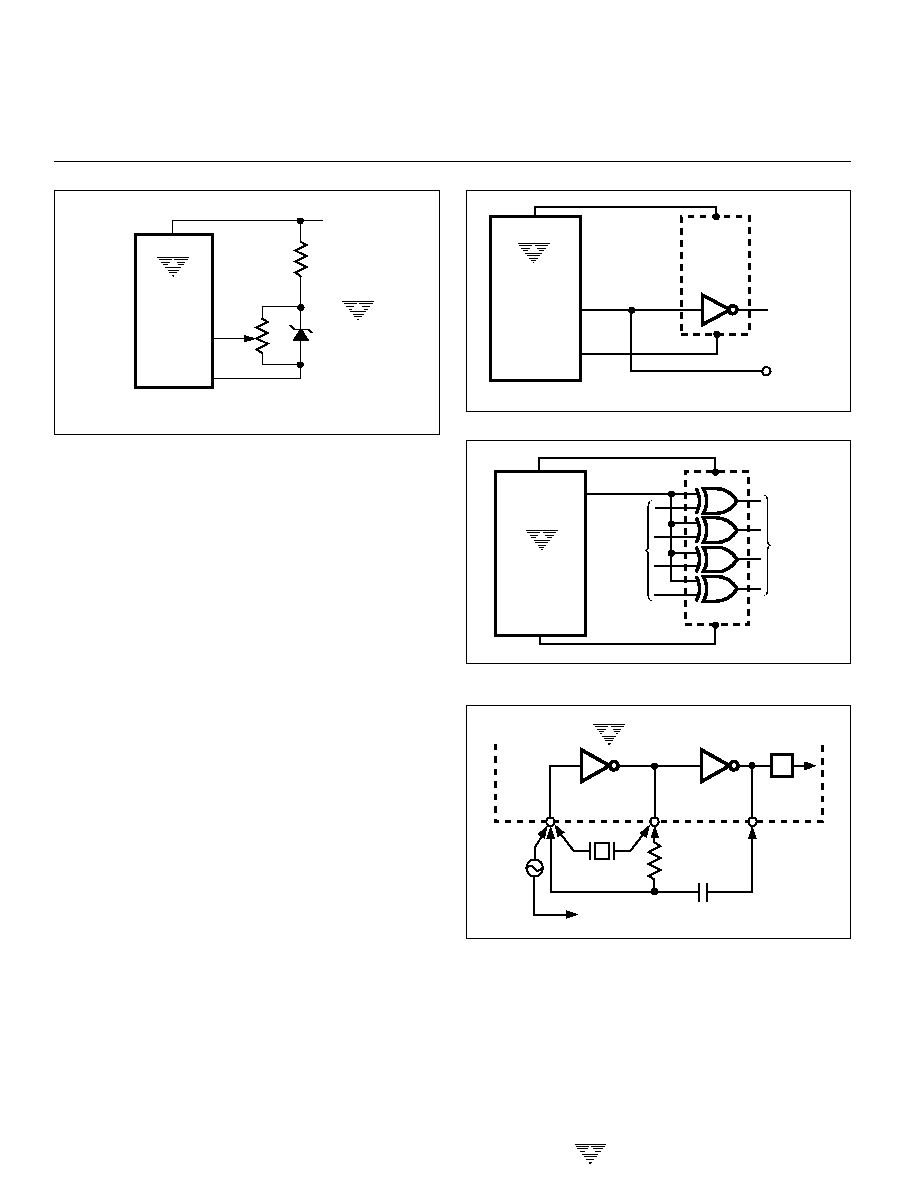
TEST
The TEST pin serves two functions. On the TC7117/
TC7117A, it is coupled to the internally-generated digital
supply through a 500
resistor. Thus, it can be used as a
Figure 7. Clock Circuits
TC7116/TC7116A
TC7117/TC7117A
TO
COUNTER
CRYSTAL
RC NETWORK
40
38
EXT
OSC
39
TO TEST PIN ON TC7116/TC7116A
TO GROUND PIN ON TC7117/TC7117A
Figure 6. Exclusive "OR" Gate for Decimal Point Drive
TC7116
TC7116A
DECIMAL
POINT
SELECT
V
+
V
+
TEST
GND
4030
TO LCD
DECIMAL
POINTS
BP
Figure 5. Simple Inverter for Fixed Decimal Point
3-1/2 DIGIT ANALOG-TO-DIGITAL
CONVERTERS WITH HOLD
TC7116
TC7116A
TC7117
TC7117A

3-211
TELCOM SEMICONDUCTOR, INC.
7
6
5
4
3
1
2
8
negative supply for externally-generated segment drivers,
such as decimal points or any other presentation the user
may want to include on the LCD. (Figures 5 and 6 show
such an application.) No more than a 1 mA load should be
applied.
The second function is a "lamp test." When TEST is
pulled HIGH (to V
+
), all segments will be turned ON and
the display should read ≠1888. The TEST pin will sink
about 10 mA under these conditions.
DIGITAL SECTION
Figures 8 and 9 show the digital section for TC7116/
TC7116A and TC7117/TC7117A, respectively. For the
TC7116/TC7116A (Figure 8), an internal digital ground is
generated from a 6V zener diode and a large P-channel
source follower. This supply is made stiff to absorb the
relative large capacitive currents when the backplane (BP)
voltage is switched. The BP frequency is the clock fre-
quency 800. For 3 readings per second, this is a 60-Hz
square wave with a nominal amplitude of 5V. The seg-
ments are driven at the same frequency and amplitude,
and are in-phase with BP when OFF, but out-of-phase
when ON. In all cases, negligible DC voltage exists across
the segments.
Figure 9 is the digital section of the TC7117/TC7117A.
It is identical to the TC7116/TC7116A, except that the
regulated supply and BP drive have been eliminated, and
the segment drive is typically 8 mA. The 1000's output (pin
19) sinks current from two LED segments, and has a 16-mA
drive capability. The TC7117/TC7117A are designed to
drive common anode LED displays.
In both devices, the polarity indication is ON for analog
inputs. If V
≠
IN
and V
+
IN
are reversed, this indication can be
reversed also, if desired.
Figure 8. TC7116/TC7116A Digital Section
TC7116
TC7116A
LCD PHASE DRIVER
THOUSANDS
HUNDREDS
TENS
UNITS
4
BACKPLANE
21
39
37
OSC
INTERNAL DIGITAL GROUND
V
+
V
≠
TEST
6.2V
500
26
35
TO SWITCH DRIVERS
FROM COMPARATOR OUTPUT
CLOCK
VTH = 1V
7-SEGMENT
DECODE
7-SEGMENT
DECODE
7-SEGMENT
DECODE
200
40
38
TYPICAL SEGMENT OUTPUT
INTERNAL DIGITAL GROUND
SEGMENT
OUTPUT
V
+
0.5 mA
2 mA
LATCH
2
OSC3
OSC1
˜
˜
HLDR
70 k
LOGIC CONTROL
1
3-1/2 DIGIT ANALOG-TO-DIGITAL
CONVERTERS WITH HOLD
TC7116
TC7116A
TC7117
TC7117A

3-212
TELCOM SEMICONDUCTOR, INC.
3-1/2 DIGIT ANALOG-TO-DIGITAL
CONVERTERS WITH HOLD
TC7116
TC7116A
TC7117
TC7117A
TC7117
TC7117A
THOUSANDS
HUNDREDS
TENS
UNITS
4
39
OSC
V
DIGITAL
GND
TEST
35
TO SWITCH DRIVERS
FROM COMPARATOR OUTPUT
CLOCK
7-SEGMENT
DECODE
7-SEGMENT
DECODE
7-SEGMENT
DECODE
40
38
2
OSC3
OSC1
˜
HLDR
CONTROL LOGIC
TYPICAL SEGMENT OUTPUT
DIGITAL GROUND
TO
SEGMENT
V
+
0.5 mA
8 mA
37
21
500
V
+
1
LATCH
~70 k
+
System Timing
The clocking method used for the TC7116/TC7116A
and TC7117/TC7117A is shown in Figure 9. Three clocking
methods may be used:
(1) An external oscillator connected to pin 40.
(2) A crystal between pins 39 and 40.
(3) An RC network using all three pins.
The oscillator frequency is
4 before it clocks the
decade counters. It is then further divided to form the three
convert-cycle phases: signal integrate (1000 counts), refer-
ence deintegrate (0 to 2000 counts), and auto-zero (1000 to
3000 counts). For signals less than full scale, auto-zero gets
the unused portion of reference deintegrate. This makes a
complete measure cycle of 4000 (16,000 clock pulses)
independent of input voltage. For 3 readings per second, an
oscillator frequency of 48 kHz would be used.
To achieve maximum rejection of 60-Hz pickup, the
signal-integrate cycle should be a multiple of 60 Hz. Oscil-
lator frequencies of 240 kHz, 120 kHz, 80 kHz, 60 kHz, 48
kHz, 40 kHz, etc. should be selected. For 50 Hz rejection,
oscillator frequencies of 200 kHz, 100 kHz, 66-2/3 kHz, 50
kHz, 40 kHz, etc. would be suitable. Note that 40 kHz (2.5
readings per second) will reject both 50 Hz and 60 Hz.
HOLD Reading Input
When HLDR is at a logic HIGH the latch will not be
updated. Analog-to-digital conversions will continue but will
not be updated until HLDR is returned to LOW. To continu-
ously update the display, connect to test (TC7116/TC7116A)
or ground (TC7117/TC7117A), or disconnect. This input is
CMOS compatible with 70 k
typical resistance to TEST
(TC7116/TC7116A) or ground (TC7117/TC7117A).
Figure 9. TC7117/TC7117A Digital Section
3-213
TELCOM SEMICONDUCTOR, INC.
7
6
5
4
3
1
2
8
3-1/2 DIGIT ANALOG-TO-DIGITAL
CONVERTERS WITH HOLD
TC7116
TC7116A
TC7117
TC7117A
COMPONENT VALUE SELECTION
Auto-Zero Capacitor
The size of the auto-zero capacitor has some influ-
ence on system noise. For 200 mV full scale, where noise
is very important, a 0.47
µ
F capacitor is recommended. On
the 2V scale, a 0.047
µ
F capacitor increases the speed of
recovery from overload and is adequate for noise on this
scale.
Reference Capacitor
A 0.1
µ
F capacitor is acceptable in most applications.
However, where a large common-mode voltage exists (i.e.,
the V
≠
IN
pin is not at analog common), and a 200-mV scale
is used, a larger value is required to prevent roll-over error.
Generally, 1
µ
F will hold the roll-over error to 0.5 count in
this instance.
Integrating Capacitor
The integrating capacitor should be selected to give the
maximum voltage swing that ensures tolerance build-up will
not saturate the integrator swing (approximately 0.3V from
either supply). In the TC7116/TC7116A or the TC7117/
TC7117A, when the analog common is used as a reference,
a nominal
±
2V full- scale integrator swing is acceptable. For
the TC7117/TC7117A, with
±
5V supplies and analog com-
mon tied to supply ground, a
±
3.5V to
±
4V swing is nominal.
For 3 readings per second (48 kHz clock), nominal values
for C
INT
are 0.22
µ
1F and 0.10
µ
F, respectively. If different
oscillator frequencies are used, these values should be
changed in inverse proportion to maintain the output swing.
The integrating capacitor must have low dielectric ab-
sorption to prevent roll-over errors. Polypropylene capaci-
tors are recommended for this application.
Integrating Resistor
Both the buffer amplifier and the integrator have a class
A output stage with 100
µ
A of quiescent current. They can
supply 20
µ
A of drive current with negligible nonlinearity.
The integrating resistor should be large enough to remain
in this very linear region over the input voltage range, but
small enough that undue leakage requirements are not
placed on the PC board. For 2V full scale, 470 k
is near
optimum and, similarly, 47 k
for 200 mV full scale.
Oscillator Components
For all frequency ranges, a 100-k
resistor is recom-
mended; the capacitor is selected from the equation:
For a 48 kHz clock (3 readings per second), C = 100 pF.
Figure 10. Negative Power Supply Generation With TC7660
V
REF
+
V
+
TC7117
TC7117A
36
10 µF
V
IN
+
V
IN
≠
COM
GND
32
31
30
21
10 µF
V
IN
V
≠
(≠5V)
5
3
8
2
4
+5V
35
TC7660
26
+
+
+
≠
TC04
LED
DRIVE
Reference Voltage
To generate full-scale output (2000 counts), the analog
input requirement is V
IN
= 2 V
REF
. Thus, for the 200 mV and
2V scale, V
REF
should equal 100 mV and 1V, respectively.
In many applications, where the ADC is connected to a
transducer, a scale factor exists between the input voltage
and the digital reading. For instance, in a measuring system
the designer might like to have a full-scale reading when the
voltage from the transducer is 700 mV. Instead of dividing
the input down to 200 mV, the designer should use the input
voltage directly and select V
REF
= 350 mV. Suitable values
for integrating resistor and capacitor would be 120 k
and
0.22
µ
F. This makes the system slightly quieter and also
avoids a divider network on the input. The TC7117/TC7117A,
with
±
5V supplies, can accept input signals up to
±
4V.
Another advantage of this system is when a digital reading
of zero is desired for V
IN
0. Temperature and weighing
systems with a variable tare are examples. This offset
reading can be conveniently generated by connecting the
voltage transducer between V
+
IN
and analog common, and
the variable (or fixed) offset voltage between analog com-
mon and V
≠
IN
.
TC7117/TC7117A POWER SUPPLIES
The TC7117/TC7117A are designed to operate from
±
5V supplies. However, if a negative supply is not available,
it can be generated with a TC7660 DC-to-DC converter and
two capacitors. Figure 10 shows this application.
In selected applications, a negative supply is not re-
quired. The conditions for using a single +5V supply are:
(1) The input signal can be referenced to the center of
the common-mode range of the converter.
(2) The signal is less than
±
1.5V.
(3) An external reference is used.
45
RC
f =
.
3-214
TELCOM SEMICONDUCTOR, INC.
3-1/2 DIGIT ANALOG-TO-DIGITAL
CONVERTERS WITH HOLD
TC7116
TC7116A
TC7117
TC7117A
TYPICAL APPLICATIONS
Figure 13. Circuit for Developing Underrange and Overrange
Signals from TC7116/TC7116A Outputs
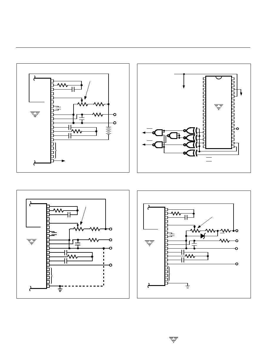
Figure 12. TC7117/TC7117A Internal Reference (200 mV Full Scale,
3 RPS, V
≠
IN
Tied to GND for Single-Ended Inputs.)
100 k
100 pF
0.47 µF
47 k
0.22 µF
TO DISPLAY
TO BACKPLANE
0.1 pF
21
1 k
22 k
9V
SET VREF= 100 mV
TC7116
TC7116A
0.01 µF
+
IN
1 M
≠
22
23
24
25
26
27
28
29
30
31
32
33
34
35
36
37
38
39
40
+
≠
21
20
40
35
26
TO
LOGIC
GND
≠
V
TO
LOGIC
VCC
+
V
CD4077
U/R
O/R
CD4023
OR 74C10
TC7116
TC7116A
O/R = OVERRANGE
U/R = UNDERRANGE
100 pF
0.47 µF
47 k
TO DISPLAY
0.1 pF
1 k
V
SET VREF= 100 mV
+
10 k
10 k
1.2V
0.01 µF
≠
IN
1 M
+
100 k
V
≠
0.22 µF
21
22
23
24
25
26
27
28
29
30
31
32
33
34
35
36
37
38
39
40
TC9491CZM
TC7117
TC7117A
100 k
100 pF
0.47 µF
47 k
0.22 µF
TO DISPLAY
0.1 pF
21
1 k
22 k
SET VREF = 100 mV
0.01 µF
+
IN
1 M
≠
22
23
24
25
26
27
28
29
30
31
32
33
34
35
36
37
38
39
40
≠5V
+5V
TC7117
TC7117A
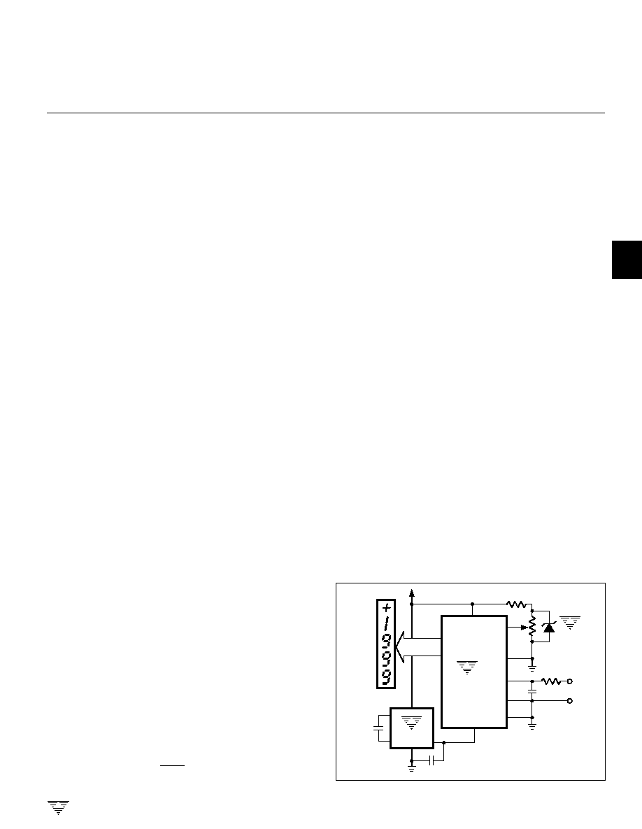
Figure 11. TC7116/TC7116A Using the Internal Reference
(200 mV Full Scale, 3 Readings Per Second (RPS)
Figure 14. TC7117/TC7117A With a 1.2V External Band-Gap
Reference (V
≠
IN
Tied to Common)

3-215
TELCOM SEMICONDUCTOR, INC.
7
6
5
4
3
1
2
8
3-1/2 DIGIT ANALOG-TO-DIGITAL
CONVERTERS WITH HOLD
TC7116
TC7116A
TC7117
TC7117A
APPLICATIONS INFORMATION
The TC7117/TC7117A sink the LED display current,
causing heat to build up in the IC package. If the internal
voltage reference is used, the changing chip temperature
can cause the display to change reading. By reducing the
LED common anode voltage, the TC7117/TC7117A pack-
age power dissipation is reduced.
Figure 17 is a curve-tracer display showing the relation-
ship between output current and output voltage for typical
TC7117CPL/TC7117ACPL devices. Since a typical LED
has 1.8V across it at 8 mA and its common anode is
connected to +5V, the TC7117/TC7117A output is at 3.2V
(Point A, Figure 17). Maximum power dissipation is 8.1 mA
◊
3.2V
◊
24 segments = 622 mW.
However, notice that once the TC7117/TC7117A's out-
put voltage is above 2V, the LED current is essentially
constant as output voltage increases. Reducing the output
voltage by 0.7V (Point B Figure 17) results in 7.7 mA of LED
current, only a 5% reduction. Maximum power dissipation is
now only 7.7 mA
◊
2.5V
◊
24 = 462 mW, a reduction of 26%.
An output voltage reduction of 1V (Point C) reduces LED
current by 10% (7.3 mA), but power dissipation by 38% (7.3
mA
◊
2.2V
◊
24 = 385 mW).
Reduced power dissipation is very easy to obtain.
Figure 18 shows two ways: Either a 5.1
, 1/4W resistor, or
a 1A diode placed in series with the display (but not in series
with the TC7117/TC7117A). The resistor reduces the
TC7117/TC7117A's output voltage (when all 24 segments
are ON) to Point C of Figure 17. When segments turn off, the
output voltage will increase. The diode, however, will result
in a relatively steady output voltage, around Point B.
In addition to limiting maximum power dissipation, the
resistor reduces change in power dissipation as the display
changes. The effect is caused by the fact that, as fewer
segments are ON, each ON output drops more voltage and
current. For the best case of six segments (a "111" display)
to worst case (a "1888" display), the resistor circuit will
change about 230 mW, while a circuit without the resistor will
change about 470 mW. Therefore, the resistor will reduce
the effect of display dissipation on reference voltage drift by
about 50%.
The change in LED brightness caused by the resistor is
almost unnoticeable as more segments turn off. If display
brightness remaining steady is very important to the de-
signer, a diode may be used instead of the resistor.
Figure 15. Recommended Component Values for 2V Full Scale
(TC7116/TC7116A and TC7117/TC7117A)
Figure 16. TC7117/TC7117A Operated from Single +5V Supply
(An External Reference Must Be Used in This
Application.)
100 k
100 pF
0.047 µF
470 k
0.22 µF
TO DISPLAY
0.1 µF
25 k
24 k
V
+
SET VREF = 1V
0.01 µF
+
IN
1M
≠
V
≠
21
22
23
24
25
26
27
28
29
30
31
32
33
34
35
36
37
38
39
40
TC7116
TC7116A
TC7117
TC7117A
100 pF
0.47 µF
47 k
TO DISPLAY
0.1 pF
1 k
V
SET VREF= 100 mV
+
10 k
10 k
1.2V
0.01 µF
≠
IN
1 M
+
100 k
0.22 µF
21
22
23
24
25
26
27
28
29
30
31
32
33
34
35
36
37
38
39
40
TC9491CZM
TC7117
TC7117A

3-216
TELCOM SEMICONDUCTOR, INC.
3-1/2 DIGIT ANALOG-TO-DIGITAL
CONVERTERS WITH HOLD
TC7116
TC7116A
TC7117
TC7117A
TP2
TP5
100
k
TP1
24 k
1 k
0.1
µF
TP3
0.01
µF
+
IN
≠
0.22
µF
DISPLAY
DISPLAY
100
pF
+5V
1 M
≠5V
150 k
0.47
µF
TC7117
TC7117A
40
TP
4
30
35
21
20
10
1
47
k
1N4001
1.5
, 1/4W
Figure 18. Diode or Resistor Limits Package Power Dissipation
Figure 17. TC7117/TC7117A Output Current vs Output Voltage