Äîêóìåíòàöèÿ è îïèñàíèÿ www.docs.chipfind.ru
1
PRELIMINARY INFORMATION
TCL1117-05 6/5/97
800mA LOW DROPOUT POSITIVE REGULATORS
ADJUSTABLE AND FIXED 2.85V, 3.30V, 5.00V
TCL1117
TCL1117-2.85
TCL1117-3.30
TCL1117-5.00
800mA LOW DROPOUT POSITIVE REGULATORS
ADJUSTABLE AND FIXED 2.85V, 3.30V, 5.00V
GENERAL DESCRIPTION
The TCL1117 is a low-dropout positive voltage regula-
tor (LDO) with 800mA output current capability. It is available
in fixed and adjustable output voltage versions, 2.85V (ac-
tive SCSI terminators), 3.30V and 5.00V. Output/reference
voltage accuracy is guaranteed to
±
1.0%. Over-current
protection is integrated onto the chip. Dropout is specified
at 1.2V maximum at full rated output current and less than
1.0V at low loads (<100mA). The SOT-223 package makes
the TCL1117 especially attractive for tight physical layouts.
For stability, a 10
µ
F output capacitor is required. The
TCL1117 is an NPN-based design which has significantly
lower unused quiescent current than similar PNP-based
regulators.
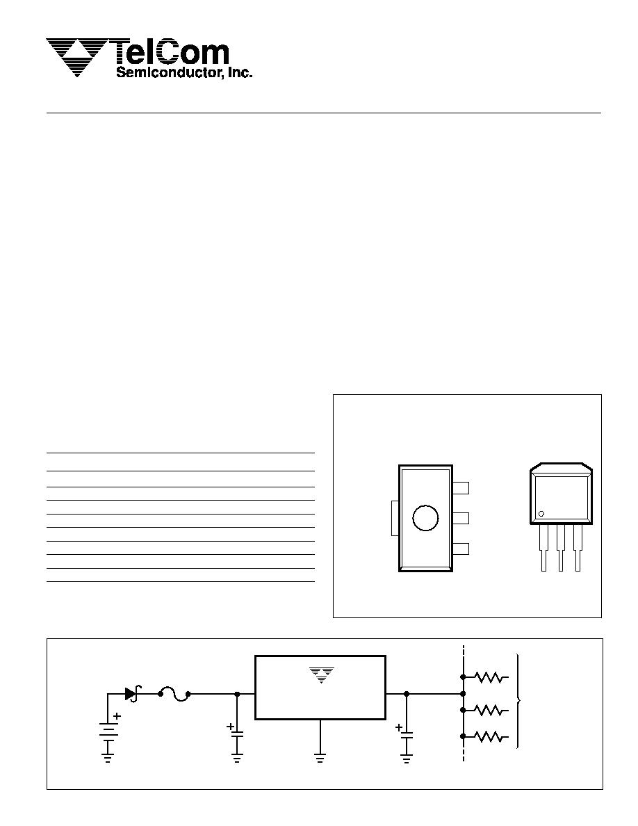
PIN CONFIGURATIONS
ADJ/GND
ADJ/GND
IN
OUT
OUT
IN
TAB IS V
OUT
FRONT VIEW
FRONT VIEW
1
1
2
3
3
2
TYPICAL APPLICATION
FEATURES
s
Space-saving SOT-223 Package
s
Pin Compatible with Older Adjustable 3 Terminal
Regulators
s
Adjustable or Fixed Voltages of 2.85V, 3.30V or 5.00V
s
High Output Current ..................................... 800mA
s
Low Dropout Voltage ............ 1.2V at I
OUT
= 800mA
s
Guaranteed Dropout Voltage at Multiple Current
Levels
s
Line Regulation (Max) ...................................... 0.2%
s
Load Regulation (Max) ..................................... 0.4%
APPLICATIONS
s
Active SCSI Terminators
s
High Efficiency Linear Regulators
s
Post Regulators for Switching Supplies
s
Battery Chargers
s
5V - 3.3V Linear Regulators
ORDERING INFORMATION
Part Number*
Package
Part Marking
TCL1117-ADJCDB
SOT-223-3
1117
TCL1117-2.85CDB
SOT-223-3
11172
TCL1117-3.30CDB
SOT-223-3
11173
TCL1117-5.00CDB
SOT-223-3
11175
TCL1117-ADJCEB
DDPAK-3
TCL1117-2.85CEB
DDPAK-3
TCL1117-3.30CEB
DDPAK-3
TCL1117-5.00CEB
DDPAK-3
*Ambient temperature range is determined by maximum operating
power dissipation and a maximum die temperature of 125
°
C (see Power
Dissipation and Thermal Design Section).
TCL1117
TCL1117-2.85
TCL1117-3.30
TCL1117-5.00
SOT-223
3-Lead Package
DDPAK-3
10
µ
F
IN
GND
OUT
TCL1117-5.00
4.75V to 5.25V
22
µ
F
110
18 to 27
LINES
110
110
Active Terminator for SCSI-2 Bus
TelCom Semiconductor reserves the right to make changes in the circuitry and specifications of its devices.
2
PRELIMINARY INFORMATION
TCL1117-05 6/5/97
TCL1117
TCL1117-2.85
TCL1117-3.30
TCL1117-5.00
800mA LOW DROPOUT POSITIVE REGULATORS
ADJUSTABLE AND FIXED 2.85V, 3.30V, 5.00V
ABSOLUTE MAXIMUM RATINGS*
Input Voltage
Operating Voltage:
TCL1117, TCL1117-3.30, TCL1117-5.00 ...... 15V
TCL1117-2.85 ................................................ 10V
Surge Voltage:
TCL1117, TCL1117-3.30, TCL1117-5.00 ...... 20V
Operating Junction Temperature ............... 0
°
C to +125
°
C
ELECTRICAL CHARACTERISTICS
Symbol
Parameter
Test Conditions
Min
Typ
Max Unit
Reference
TCL1117
I
OUT
= 10mA, (V
IN
V
OUT
) = 2V, T
J
= 25
°
C
1.238 1.250 1.262
V
Voltage
10
I
OUT
800mA, 1.4V
(V
IN
V
OUT
)
10V (Note 1) 1.225 1.250 1.270
Output Voltage
TCL1117-2.85
I
OUT
= 10mA, V
IN
= 4.85V, T
J
= 25
°
C
2.820 2.850 2.880
V
0
I
OUT
800mA, 4.25V
V
IN
10V (Note 1)
2.790 2.850 2.910
0
I
OUT
500mA, V
IN
= 3.95V (Note 1)
2.790 2.850 2.910
TCL1117-3.30
I
OUT
= 10mA, V
IN
= 5.3V, T
J
= 25
°
C
3.265 3.300 3.335
V
0
I
OUT
800mA, 4.75V
V
IN
10V (Note 1)
3.230 3.300 3.370
TCL1117-5.00
I
OUT
= 10mA, V
IN
= 7V, T
J
= 25
°
C
4.950 5.000 5.050
V
0
I
OUT
800mA, 6.50V
V
IN
12V (Note 1)
4.900 5.000 5.100
Line Regulation
TCL1117
I
OUT
= 10mA, 1.5V
V
IN
V
OUT
15V (Notes 1 & 2)
--
0.035
0.2
%
TCL1117-2.85
I
OUT
= 0mA, 4.25V
V
IN
10V (Notes 1 & 2)
--
1
6
mV
TCL1117-3.30
I
OUT
= 0mA, 4.75V
V
IN
15V (Notes 1 & 2)
--
1
7
TCL1117-5.00
I
OUT
= 0mA, 6.5V
V
IN
15V (Notes 1 & 2)
--
1
10
Load Regulation
TCL1117
(V
IN
V
OUT
) = 3V, 10mA,
I
OUT
800mA (Notes 1 & 2)
--
0.1
0.4
%
TCL1117-2.85
V
IN
= 4.25V, 0
I
OUT
800mA (Notes 1 & 2)
--
1
10
mV
TCL1117-3.30
V
IN
= 4.75V, 0
I
OUT
800mA (Notes 1 & 2)
--
1
12
TCL1117-5.00
V
IN
= 6.5V, 0
I
OUT
800mA (Notes 1 & 2)
--
1
15
Dropout Voltage
I
OUT
= 100mA, (Note 1 & 3)
--
1.00
1.10
V
I
OUT
= 500mA, (Note 1 & 3)
--
1.05
1.15
I
OUT
= 800mA, (Note 1 & 3)
--
1.10
1.20
Current Limit
(V
IN
V
OUT
) = 5V, T
J
= 25
°
C
800
950
1200
mA
Minimum Load
TCL1117
(V
IN
V
OUT
) = 15V (Note 1 & 4)
--
1.7
5
mA
Current
Quiescent
TCL1117-2.85
V
IN
10V (Note 1)
--
5
10
mA
Current
TCL1117-3.30
V
IN
15V (Note 1)
--
5
10
TCL1117-5.00
V
IN
15V (Note 1)
--
5
10
Thermal Regulation
T
A
= 25
°
C, 30msec Pulse
--
0.01
0.1
%W
Ripple Rejection
f
RIPPLE
= 120Hz (V
IN
V
OUT
) = 3V, V
RIPPLE
= 1Vp-p ( Note 1)
60
75
--
dB
Adjust Pin Current
(Note 1)
--
55
120
µ
A
Adjust Pin Current Change
10mA
I
OUT
800mA, 1.4V
(V
IN
V
OUT
)
10V (Note 1)
--
0.2
5
µ
A
Temperature Stability
--
0.5
--
%
Long Term Stability
T
A
= 125
°
C, 1000 Hrs.
--
0.3
--
%
RMS Output Noise
(% of V
OUT
)
,
10Hz
f
10kHz
--
0.003
--
%
Thermal Resistance
(Junction to Case, at Tab)
--
15
--
°
C/W
NOTES: 1. Specifications apply over the full operating temperature range.
2. See thermal regulation specification for changes in output voltage due to heating effects. Load regulation and line regulation are
measured at a constant junction temperature by low duty cycle pulse testing.
3. Dropout voltage is specified over the full output current range of the device. Dropout voltage is defined as the minimum input/output
differential measured at the specified output current. Test points and limits are also shown on the Dropout Voltage curve.
4. Minimum load current is defined as the minimum output current required to maintain regulation.
Storage Temperature ............................ 65
°
C to +150
°
C
Lead Temperature (Soldering 10 sec) .................... 300
°
C
*Stresses beyond those listed under "Absolute Maximum Ratings" may
cause permanent damage to the device. These are stress ratings only, and
functional operation of the device at these or any other conditions beyond
those indicated in the operational sections of the specifications is not
implied. Exposure to absolute maximum rating conditions for extended
periods may affect device reliability.
3
PRELIMINARY INFORMATION
TCL1117-05 6/5/97
800mA LOW DROPOUT POSITIVE REGULATORS
ADJUSTABLE AND FIXED 2.85V, 3.30V, 5.00V
TCL1117
TCL1117-2.85
TCL1117-3.30
TCL1117-5.00
APPLICATIONS
Overload Protection
The TCL1117 is protected against current (short-circuit)
and thermal overload conditions. Thermal protection is
triggered by a chip temperature exceeding 165
°
C. Current
overload is triggered at approximately 950mA.
Stability and Load Regulation
The TCL1117 requires a capacitor from V
OUT
to GND to
provide compensation feedback to the internal gain stage.
This is to ensure stability at the output terminal. Typically, a
10
µ
F tantalum or 50
µ
F aluminum electrolytic is sufficient.
NOTE: It is important that the ESR for this capacitor does not
exceed 0.5
.
The output capacitor does not have a theoretical upper
limit and increasing its value will increase stability.
C
OUT
= 100
µ
F or more is typical for high current regulator
designs. NOTE: See Protection Diodes for limitations. An-
other benefit of larger output capacitance is improved tran-
sient load response (large di/dt in the load).
Protection Diodes
Typically no protection diodes are necessary for the
TCL1117. Unlike older regulators, the ADJ pin is protected
internally from excessive currents. The ADJ pin can be
driven with voltage transients as high as
±
25V with respect
to the output without damage to the device.
Likewise, a diode between the input and output is not
typically required. If the input voltage collapses the internal
circuitry can absorb ~20A transient currents (<10
µ
sec)
without damage. This reverse current is much larger than
most power supply designs can generate. However, if the
output capacitor is VERY large (>1000
µ
F), instantaneous
currents can be high enough to damage the chip. In this
case, a high-current, fast-response diode is recommended.
(See Figure 1).
Output Voltage Adjust
Like most LDOs, the TCL1117 regulates the output by
comparing the output voltage, or a multiple thereof, to an
internally generated reference voltage. On the adjustable
version, the V
REF
is available externally as 1.25V (
±
1%)
between V
OUT
and ADJ (See Figure 2). The voltage divider
formed by R1 and R2 should be set to conduct 10mA
(minimum output load). The output voltage is given by the
following equation:
V
OUT
= V
REF
(
1+ R2
)
+ I
ADJ
R2
R1
On fixed voltage versions of the TCL1117, the voltage
divider is provided internally.
Load Regulation
The TCL1117 load regulation is limited by the resistance
of the wire connecting it to the load (R
p
, Figure 3). For the
adjustable version, the best load regulation is accomplished
when the top of the resistor divider (R1) is connected directly
to the output pin of the TCL1117, NOT to the high side of the
load (Figure 3). When so connected, R
p
is not multiplied by
the divider ratio. For the fixed output versions, the top of R1
is internally connected to the output and the ground pin can
be connected to the low side of the load as a negative side
sense if, so desired.
Figure 1.
Figure 2. Basic Adjustable Regulator
+
+
VOUT
CADJ
10
µ
F
COUT
150
µ
F
R2
R1
OUT
IN
TCL1117
D1
1N4002
(OPTIONAL)
ADJ
VIN
VOUT
VREF
IADJ
50
µ
A
R2
VOUT = VREF
(
1+ R2
)
+ IADJ R2
R1
R1
OUT
IN
TCL1117
ADJ
VIN
4
PRELIMINARY INFORMATION
TCL1117-05 6/5/97
TCL1117
TCL1117-2.85
TCL1117-3.30
TCL1117-5.00
800mA LOW DROPOUT POSITIVE REGULATORS
ADJUSTABLE AND FIXED 2.85V, 3.30V, 5.00V
Table 1.
Thermal
Copper Area
Resistance
Topside* Backside Board Area
(Junction-to-Ambient)
2500 Sq. mm
2500 Sq. mm
2500 Sq. mm
45
°
C/W
1000 Sq. mm
2500 Sq. mm
2500 Sq. mm
45
°
C/W
225 Sq. mm
2500 Sq. mm
2500 Sq. mm
53
°
C/W
100 Sq. mm
2500 Sq. mm
2500 Sq. mm
59
°
C/W
1000 Sq. mm
1000 Sq. mm
1000 Sq. mm
52
°
C/W
1000 Sq. mm
0
1000 Sq. mm
55
°
C/W
*Tab of device attached to topside copper
Soldering Methods
The recommended methods of soldering the SOT-223
package are: vapor phase re-flow and infrared re-flow with
component preheat within 65
°
C of the solder temperature.
Hand soldering and wave soldering methods are not recom-
mended since they can damage the part with excessive
thermal gradients across the surface area of the package.
Thermal shock to the package (>30
°
C per second) must be
minimized.
Ripple Rejection
Ripple Rejection curves were generated using an ad-
justable output TCL1117 with a bypass capacitor from ADJ
to ground. To obtain the performance shown in the curves,
the impedance of the bypass capacitor (at the ripple fre-
quency) should be less than R1. R1 is typically 100
to
200
. For example at 120Hz, with R1 = 100
, the adjust
capacitor should be at least 13
µ
F. Only 0.16
µ
F would be
required at 10kHz.
The output ripple increases as the ratio of the output
voltage to the reference voltage (V
OUT
/V
REF
) in fixed voltage
devices, and adjustable devices without an adjust pin ca-
pacitor. For example, at 5V, output ripple will increase by a
factor of 4 (5/1.25V). Ripple rejection will be reduced by 12db
from the value shown on the curve.
Power Dissipation and Thermal Design
As mentioned earlier, the TCL1117 has thermal over-
load protection which limits internal temperature to +165
°
C.
However, device functionality is only guaranteed to a maxi-
mum junction temperature of +125
°
C. Since internal power
dissipation can be >1 watt, careful thermal design is essen-
tial. The TCL1117 is supplied in a SOT-223 package which
is intended to be directly surface-mounted to the PC-board.
Because there is no dedicated heat sink, power dissipation
to ambient is performed largely by the PC board and its
copper material.
The power dissipation and junction temperature for the
TCL1117 in a SOT-223 are given by the following equations:
P
D
= (V
IN
V
OUT
) x (I
OUT
)
T
JUNCTION
= T
AMBIENT
+ (P
D
x
JA
)
NOTE: T
JUNCTION
must not exceed 125
°
C
The
JC
(junction to external tab) for the SOT-223 is
15
°
C/W. Depending upon heatsink parameters, the
CA
can
be as low as 30
°
C/W. Therefore, the total thermal resistance
(
JA
) is at least 45
°
C/W. Table 1 shows thermal resistance
measurements taken with the TCL1117 mounted on 1/16
inch 2-layer PCB with 1oz. copper foil. NOTE: The TAB pin
does not have to be soldered to all copper layers for effective
heat transfer. Use Table 1 only as a rough guide since
thermal interactions with adjacent components cannot be
predicted.
Figure 3. Connections for Best Load Regulation
CONNECT
R1 TO CASE
CONNECT
R2 TO LOAD
Rp
PARASITIC
LINE RESISTANCE
R2
R1
RL
OUT
IN
TCL1117
ADJ
VIN
5
PRELIMINARY INFORMATION
TCL1117-05 6/5/97
800mA LOW DROPOUT POSITIVE REGULATORS
ADJUSTABLE AND FIXED 2.85V, 3.30V, 5.00V
TCL1117
TCL1117-2.85
TCL1117-3.30
TCL1117-5.00
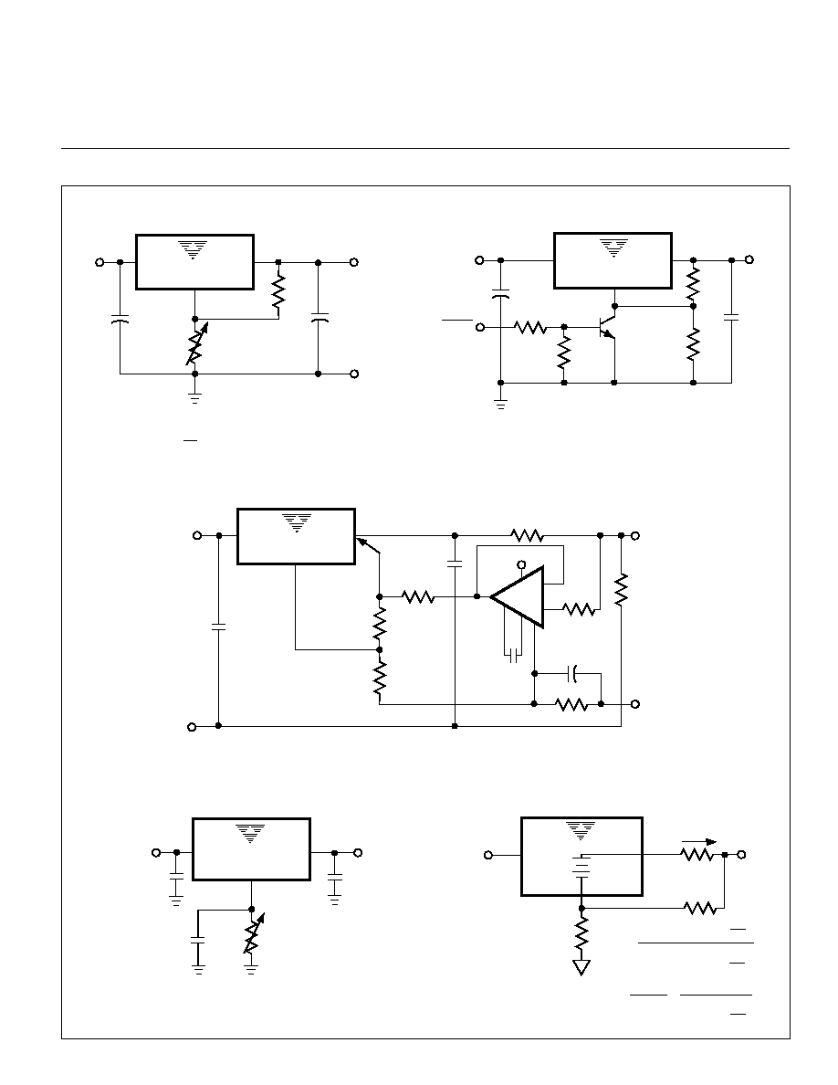
TYPICAL APPLICATIONS
R2
1k
C1*
10
µ
F
R1
121
121
25
1k
25
2
3
6
1
8
4
7
365
121
1%
365
1%
OUT
IN
1.2V-10V Adjustable Regulator
Remote Sensing
* NEEDED IF DEVICE IS FAR FROM FILTER CAPACITORS
** VOUT = 1.25V
(
1+ R2
)
ADJ
TCL1117
VIN
VOUT**
C2
100
µ
F
RETURN
RETURN
Rp
(MAX DROP 300mV)
OUT
IN
TCL1117
LM301A
ADJ
VIN
RL
OUTPUT
5V
VIN
10
µ
F
100
µ
F
5
µ
F
100pF
+
+
1k
1k
SHDN
5V
100
µ
F
2N3904
10
µ
F
OUT
IN
5V Regulator with Shutdown
ADJ
VIN
+
+
R1
+
+
+
TCL1117
+
1k
OUT
IN
Adjusting Output Voltage of Fixed Regulators
*OPTIONAL IMPROVES RIPPLE REJECTION
GND
TCL1117-5.00
10
µ
F*
100
µ
F
10
µ
F
5V TO 10V
+
VIN > 12V
VOUT
+
+
OUT
IF
RS
R1
IN
Battery Charger
ADJ
1.25V
TCL1117
VIN
R2
VOUT 1.25V
(
1+ R2
)
RS
(
1+ R2
)
R1
R1
R1
IF =
IF
VOUT
RS
(
1+ R2
)
=
1
Document Outline
- Return to Contents
- List of Figures
- 1.
- 2. Basic Adjustable Regulator
- 3. Connections for Best Load Regulation
- List of Tables
- Features
- Applications
- Ordering Information
- Typical Applications
- General Description
- Pin Configurations
- Absolute Maximum Ratings*
- Electrical Characteristics
- Applications
- Overload Protection
- Stability and Load Regulation
- Protection Diodes
- Output Voltage Adjust
- Load Regulation
- Power Dissipation and Thermal Design
- Soldering Methods
- Ripple Rejection
- Typical Applications
- Typical Characteristics
- Package Dimensions
- Sales Offices