 | –≠–ª–µ–∫—Ç—Ä–æ–Ω–Ω—ã–π –∫–æ–º–ø–æ–Ω–µ–Ω—Ç: BPW14NC | –°–∫–∞—á–∞—Ç—å:  PDF PDF  ZIP ZIP |
BPW14N
TELEFUNKEN Semiconductors
Rev. A2, 15-Jul-96
1 (6)
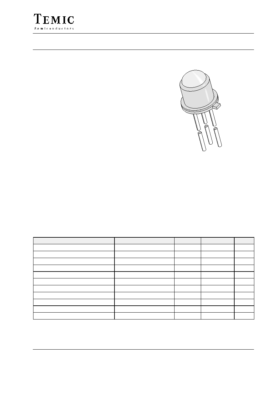
Silicon NPN Phototransistor
Description
BPW14N is a high speed silicon NPN epitaxial planar
phototransistor in a standard TO≠18 hermetically sealed
metal case.
Its glass lens, featuring a viewing angle of
±
12
∞ makes it
insensible to ambient straylight. A base terminal is avail-
able to enable biasing and sensitivity control.
Features
D Hermetically sealed case
D Lens window
D Narrow viewing angle
=
±
10
∞
D Exact central chip alignment
D Base terminal available
D High photo sensitivity
D Fast response times
D Suitable for visible and near infrared radiation
D Selected into sensitivity groups
94 8486
Applications
Detector in electronic control and drive circuits
Absolute Maximum Ratings
T
amb
= 25
_C
Parameter
Test Conditions
Symbol
Value
Unit
Collector Base Voltage
V
CBO
32
V
Collector Emitter Voltage
V
CEO
32
V
Emitter Base Voltage
V
EBO
5
V
Collector Current
I
C
50
mA
Peak Collector Current
t
p
/T = 0.5, t
p
x 10 ms
I
CM
100
mA
Total Power Dissipation
T
amb
x 25 ∞C
P
tot
310
mW
Junction Temperature
T
j
150
∞C
Storage Temperature Range
T
stg
≠55...+150
∞C
Soldering Temperature
t
x 5 s
T
sd
260
∞C
Thermal Resistance Junction/Ambient
R
thJA
400
K/W
Thermal Resistance Junction/Case
R
thJC
150
K/W

BPW14N
TELEFUNKEN Semiconductors
Rev. A2, 15-Jul-96
2 (6)
Basic Characteristics
T
amb
= 25
_C
Parameter
Test Conditions
Symbol
Min
Typ
Max
Unit
Collector Emitter Breakdown
Voltage
I
C
= 1 mA
V
(BR)CEO
32
V
Collector Dark Current
V
CE
= 20 V, E = 0
I
CEO
1
100
nA
Collector Emitter Capacitance
V
CE
= 5 V, f = 1 MHz, E=0
C
CEO
5.7
pF
Collector Base Capacitance
V
CB
= 5 V, f = 1 MHz, E=0
C
CBO
6.5
pF
Angle of Half Sensitivity
±
10
deg
Wavelength of Peak Sensitivity
l
p
780
nm
Range of Spectral Bandwidth
l
0.5
520...950
nm
Collector Emitter Saturation
Voltage
I
C
= 1 mA, I
B
= 100
mA
V
CEsat
0.3
V
Turn≠On Time
V
S
=5V, I
C
=5mA, R
L
=100
W
t
on
3.2
ms
Turn≠Off Time
V
S
=5V, I
C
=5mA, R
L
=100
W
t
off
2.7
ms
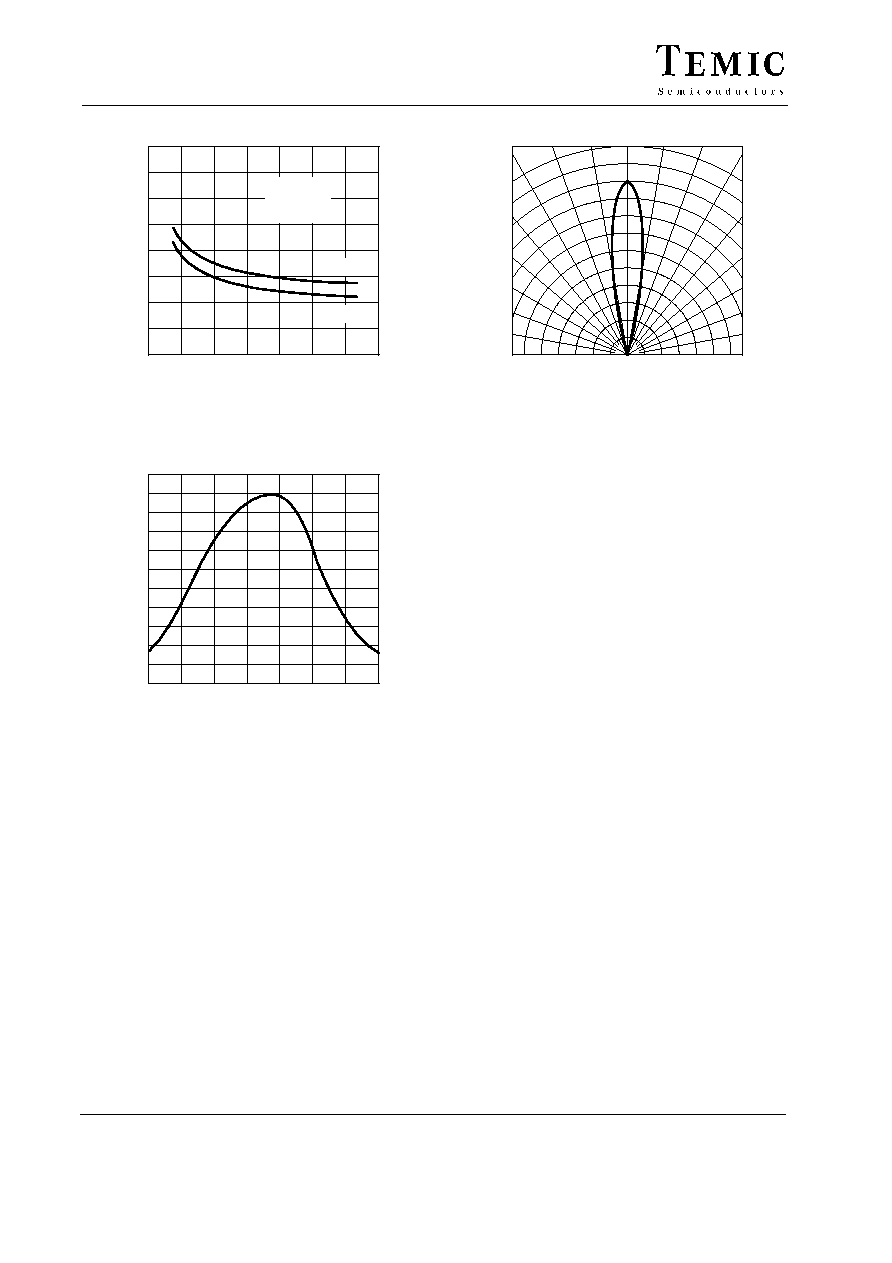
Cut≠Off Frequency
V
S
=5V, I
C
=5mA, R
L
=100
W
f
c
170
kHz
Type Dedicated Characteristics
T
amb
= 25
_C
Parameter
Test Conditions
Type
Symbol
Min
Typ
Max
Unit
Collector Light Current
E
e
=1mW/cm
2
,
l
BPW14NB
I
ca
1.0
1.5
2.0
mA
g
e
,
l=950nm, V
CE
=5V
BPW14NC
I
ca
1.7
3.0
mA

BPW14N
TELEFUNKEN Semiconductors
Rev. A2, 15-Jul-96
3 (6)
Typical Characteristics (T
amb
= 25
_C unless otherwise specified)
0
25
50
75
100
0
200
400
800
150
94 8329
600
125
T
amb
≠ Ambient Temperature (
∞
C )
P
≠
T
otal Power Dissipation ( mW
)
tot
R
thJC
R
thJA
Figure 1. Total Power Dissipation vs. Ambient Temperature
94 8330
20
I ≠ Collector Dark Current ( nA
)
CEO
T
amb
≠ Ambient Temperature (
∞
C )
10
0
10
1
10
2
10
3
10
4
10
6
10
5
150
50
100
V
CE
=20V
Figure 2. Collector Dark Current vs. Ambient Temperature
94 8331
0
50
100
150
T
amb
≠ Ambient Temperature (
∞
C )
0
0.5
1.0
1.5
2.0
3.5
I ≠ Relative Collector Current
ca rel
2.5
3.0
V
CE
=5V
E
e
=1mW/cm
2
l=950nm
Figure 3. Relative Collector Current vs. Ambient Temperature
0.01
0.1
1
0.01
0.1
1
10
I ≠ Collector Light Current ( mA
)
ca
E
e
≠ Irradiance ( mW / cm
2
)
10
94 8339
V
CE
=5V
l=950nm
BPW 14 NB
BPW 14 NC
Figure 4. Collector Light Current vs. Irradiance
0.1
1
10
0.1
1
10
I ≠ Collector Light Current ( mA
)
ca
V
CE
≠ Collector Emitter Voltage ( V )
100
94 8340
E
e
=1 mW/cm
2
0.5 mW/cm
2
0.2 mW/cm
2
0.1 mW/cm
2
l=950nm
BPW 14 NB
Figure 5. Collector Light Current vs. Collector Emitter Voltage
0.1
1
10
0
4
8
12
16
20
C ≠ Collector Emitter Capacitance ( pF )
CEO
V
CE
≠ Collector Emitter Voltage ( V )
100
94 8335
f=1MHz
Figure 6. Collector Emitter Capacitance vs.
Collector Emitter Voltage
BPW14N
TELEFUNKEN Semiconductors
Rev. A2, 15-Jul-96
4 (6)
0
2
4
6
12
0
2
8
14
94 8336
t / t ≠
T
urn on /
T
urn
of
f
T
ime ( s )
of
f
I
C
≠ Collector Current ( mA )
m
on
6
4
10
8
V
CE
=5V
R
L
=100
W
l=950nm
t
off
t
on
Figure 7. Turn On/Turn Off Time vs. Collector Current
400
600
1000
0
0.2
0.4
0.6
0.8
1.0
S ( ) ≠ Relative Spectral Sensitivity
rel
l ≠ Wavelength ( nm )
94 8337
l
800
Figure 8. Relative Spectral Sensitivity vs. Wavelength
0.4
0.2
0
0.2
0.4
S ≠ Relative Sensitivity
rel
0.6
94 8351
0.6
0.9
0.8
0
∞
30
∞
10
∞
20
∞
40
∞
50
∞
60
∞
70
∞
80
∞
0.7
1.0
Figure 9. Relative Radiant Sensitivity vs.
Angular Displacement
BPW14N
TELEFUNKEN Semiconductors
Rev. A2, 15-Jul-96
5 (6)
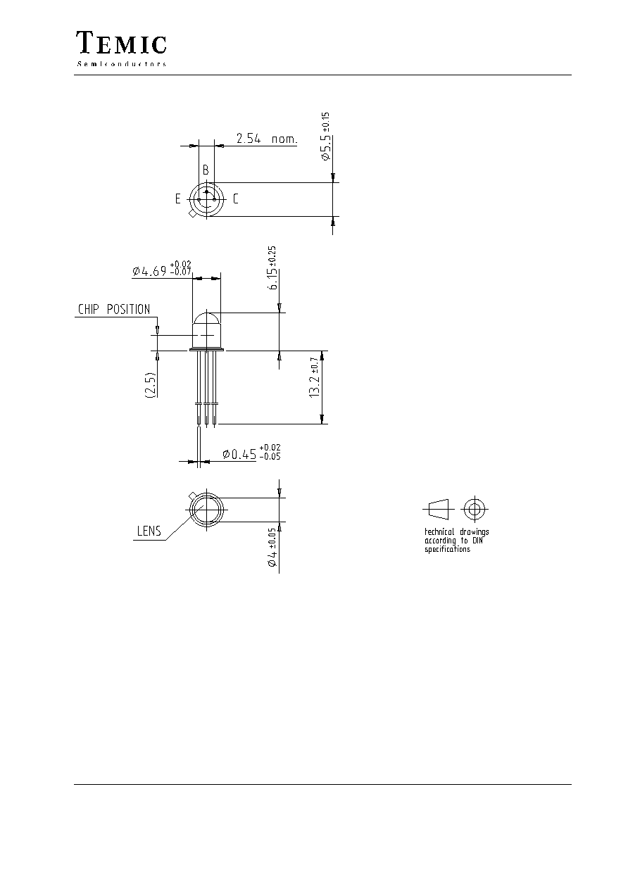
Dimensions in mm
96 12180