 | –≠–ª–µ–∫—Ç—Ä–æ–Ω–Ω—ã–π –∫–æ–º–ø–æ–Ω–µ–Ω—Ç: DG183BP | –°–∫–∞—á–∞—Ç—å:  PDF PDF  ZIP ZIP |
*Common to Substrate and Case
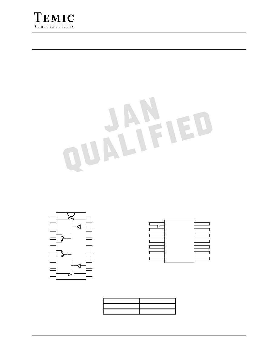
Refer to JAN38510 Information, Military Section
D
1
S
1
NC
Dual-In-Line
IN
1
D
3
V≠
S
3
V
R
S
4
V
L
D
4
V+
NC
IN
2
D
2
S
2
1
2
3
4
5
6
7
8
16
15
14
13
12
11
10
9
Top View
Flat
Package
S
4
S
3
D
4
D
3
D
2
D
1
S
2
S
1
IN
2
IN
1
V+
V≠*
V
L
V
R
1
2
3
4
5
6
7
14
13
12
11
10
9
8
Top View
DG183/184/185
Siliconix
S-52895--Rev. D, 16-Jun-97
1
High-Speed Drivers with Dual DPST JFET Switches
Features
Benefits
Applications
D Constant On-Resistance Over
Entire Analog Range
D Low Leakage
D Low Crosstalk
D Break-Before-Make Switching
D Rad Hardness
D Low Distortion
D Eliminates Large Signal Errors
D High Precision
D Improved Channel Isolation
D Eliminates Inadvertent Shorting
Between Channels
D Fault Protection
D Audio Switching
D Precision Switching
D Video Switching
D Video Routing
D Sample/Hold
D Aerospace
Description
The DG183/184/185 are precision dual double-pole,
single-throw (DPST) analog switches designed to provide
accurate switching of video and audio signals. This series
is ideally suited for applications requiring a constant
on-resistance over the entire analog range.
The major difference in the devices is the on-resistance
(DG183--10
W, DG184--30 W, DG185--75 W). Reduced
errors are achieved through low leakage current (I
D(on)
< 2 nA). Applications which benefit from the flat JFET
on-resistance include audio switching, video switching, and
data acquisition.
To achieve fast and accurate switch performance, each
device comprises four n-channel JFET transistors and a
TTL compatible bipolar driver. In the on state, each switch
conducts current equally well in either direction. In the off
condition, the switches will block up to 20 V peak-to-peak,
with feedthrough of less than ≠60 dB at 10 MHz.
Functional Block Diagram and Pin Configuration
Truth Table
Logic
Switch
0
OFF
1
ON
Logic "0"
v 0.8 V
Logic 0
v 0.8 V
Logic "1"
w 2 0 V
Logic "1"
w 2.0 V
Updates to this data sheet may be obtained via facsimile by calling Siliconix FaxBack, 1-408-970-5600. Please request FaxBack document #70032.

DG183/184/185
2
Siliconix
S-52895--Rev. D, 16-Jun-97
Ordering Information
Temp Range
Package
Part Number
≠25to 85
_C
16-Pin Sidebraze
DG183BP
≠25 to 85
_C
16-Pin Sidebraze
DG184BP
DG183AP/883
16-Pin Sidebraze
DG184AP/883,
JM38510/11103BEA
≠55 to 125
_C
DG185AP/883,
JM38510/11104BEA
14-Pin Flat Pack
JM38510/11103BXA
14-Pin Flat Pack
JM38510/11104BXA
Absolute Maximum Ratings
V+ to V≠
36 V
. . . . . . . . . . . . . . . . . . . . . . . . . . . . . . . . . . . . . . . . . . . . .
V+ to V
D
33
V
. . . . . . . . . . . . . . . . . . . . . . . . . . . . . . . . . . . . . . . . . . . . .
V
D
to V≠
33 V
. . . . . . . . . . . . . . . . . . . . . . . . . . . . . . . . . . . . . . . . . . . . .
V
D
to V
D
"22 V
. . . . . . . . . . . . . . . . . . . . . . . . . . . . . . . . . . . . . . . . . .
V
L
to V≠
36 V
. . . . . . . . . . . . . . . . . . . . . . . . . . . . . . . . . . . . . . . . . . . . .
V
L
to V
IN
8
V
. . . . . . . . . . . . . . . . . . . . . . . . . . . . . . . . . . . . . . . . . . . . .
V
L
to V
R
8
V
. . . . . . . . . . . . . . . . . . . . . . . . . . . . . . . . . . . . . . . . . . . . . .
V
IN
to V
R
8 V
. . . . . . . . . . . . . . . . . . . . . . . . . . . . . . . . . . . . . . . . . . . . . .
V
R
to V≠
27 V
. . . . . . . . . . . . . . . . . . . . . . . . . . . . . . . . . . . . . . . . . . . . . .
V
R
to V
IN
2 V
. . . . . . . . . . . . . . . . . . . . . . . . . . . . . . . . . . . . . . . . . . . . . .
Current (S or D) DG183
200 mA
. . . . . . . . . . . . . . . . . . . . . . . . . . . . . . .
Current (S or D) DG184, DG185
30 mA
. . . . . . . . . . . . . . . . . . . . . . . . .
Current (All Other Pins)
30 mA
. . . . . . . . . . . . . . . . . . . . . . . . . . . . . . . .
Storage Temperature
≠65 to 150
_C
. . . . . . . . . . . . . . . . . . . . . . . . . . . . .
Power Dissipation
a
16-Pin Sidebraze
b
900 mW
. . . . . . . . . . . . . . . . . . . . . . . . . . . . . . . . . . . .
14-Pin Flat Pack
c
900 mW
. . . . . . . . . . . . . . . . . . . . . . . . . . . . . . . . . . . .
Notes:
a.
All leads welded or soldered to PC Board.
b.
Derate 12 mW/
_C above 75_C
c.
Derate 10 mW/
_C above 75_C
Schematic Diagram (Typical Channel)
Figure 1.
V
R
V
L
V+
S
IN
D
V≠

DG183/184/185
Siliconix
S-52895--Rev. D, 16-Jun-97
3
Specifications
a
for DG183
Test Conditions
Unless Otherwise Specified
V+ = 15 V V = 15 V V = 5 V
A Suffix
≠55 to 125
_C
B Suffix
≠25 to 85
_C
Parameter
Symbol
V+ = 15 V, V≠ = ≠15 V, V
L
= 5 V
V
R
= 0 V, V
IN
= 0.8 V or 2 V
f
Temp
b
Typ
c
Min
d
Max
d
Min
d
Max
d
Unit
Analog Switch
Analog Signal Range
e
V
ANALOG
Full
≠7.5
15
≠7.5
15
V
Drain-Source
On-Resistance
r
DS(on)
I
S
= ≠10 mA, V
D
= ≠7.5 V
Room
Full
7.5
10
20
15
25
W
Source Off
L k
C
I
S(off)
V
S
=
"10 V, V
D
=
#10 V
V+ = 10 V, V≠ = ≠20 V
Room
Hot
0.05
10
1000
15
300
Leakage Current
I
S(off)
V
S
=
"7.5 V, V
D
=
#7.5 V
Room
Hot
0.05
10
1000
15
300
Drain Off
L k
C
I
D(off)
V
S
=
"10 V, V
D
=
#10 V
V+ = 10 V, V≠ = ≠20 V
Room
Hot
0.04
10
1000
15
300
nA
Leakage Current
I
D(off)
V
S
=
"7.5 V, V
D
=
#7.5 V
Room
Hot
0.03
10
1000
15
300
Channel On
Leakage Current
I
D(on)
V
D
= V
S
=
"7.5 V
Room
Hot
≠0.1
≠2
≠200
≠10
≠200
Saturation Drain Current
I
DSS
2 ms Pulse Duration
Room
300
mA
Digital Input
Input Current with
Input Voltage High
I
INH
V
IN
= 5 V
Room
Hot
<0.01
10
20
10
20
mA
Input Current with
Input Voltage Low
I
INL
V
IN
= 0 V
Full
≠30
≠250
≠250
mA
Dynamic Characteristics
Turn-On Time
t
on
See Switching Time Test Circuit
Room
240
400
600
ns
Turn-Off Time
t
off
See Switching Time Test Circuit
Room
140
200
220
ns
Source-Off Capacitance
C
S(off)
V
S
= ≠5 V, I
D
= 0
Room
21
Drain-Off Capacitance
C
D(off)
f = 1 MHz
V
D
= ≠5 V, I
S
= 0
Room
17
pF
Channel-On Capacitance
C
D(on)
V
D
= V
S
= 0 V
Room
17
Off Isolation
OIRR
f = 1 MHz, R
L
= 75
W
Room
>55
dB
Power Supplies
Positive Supply Current
I+
Room
0.6
1.5
1.5
Negative Supply Current
I≠
V
IN
= 0 V or 5 V
Room
≠2.7
≠5
≠5
mA
Logic Supply Current
I
L
V
IN
= 0 V, or 5 V
Room
3.1
4.5
4.5
mA
Reference Supply Current
I
R
Room
≠1
≠2
≠2
Notes:
a.
Refer to PROCESS OPTION FLOWCHART .
b.
Room = 25
_C, Full = as determined by the operating temperature suffix.
c.
Typical values are for DESIGN AID ONLY, not guaranteed nor subject to production testing.
d.
The algebraic convention whereby the most negative value is a minimum and the most positive a maximum, is used in this data sheet.
e.
Guaranteed by design, not subject to production test.
f.
V
IN
= input voltage to perform proper function.

DG183/184/185
4
Siliconix
S-52895--Rev. D, 16-Jun-97
Specifications
a
for DG184
Test Conditions
Unless Otherwise Specified
V+ = 15 V V = 15 V V = 5 V
A Suffix
≠55 to 125
_C
B Suffix
≠25 to 85
_C
Parameter
Symbol
V+ = 15 V, V≠ = ≠15 V, V
L
= 5 V
V
R
= 0 V, V
IN
= 0.8 V or 2 V
f
Temp
b
Typ
c
Min
d
Max
d
Min
d
Max
d
Unit
Analog Switch
Analog Signal Range
e
V
ANALOG
Full
≠7.5
15
≠7.5
15
V
Drain-Source
On-Resistance
r
DS(on)
I
S
= ≠10 mA, V
D
= ≠7.5 V
Room
Full
22
30
60
50
75
W
Source Off
L k
C
I
S(off)
V
S
=
"10 V, V
D
=
#10 V
V+ = 10 V, V≠ = ≠20 V
Room
Hot
0.06
1
100
5
100
Leakage Current
I
S(off)
V
S
=
"7.5 V, V
D
=
#7.5 V
Room
Hot
0.05
1
100
5
100
Drain Off
L k
C
I
D(off)
V
S
=
"10 V, V
D
=
#10 V
V+ = 10 V, V≠ = ≠20 V
Room
Hot
0.4
1
100
5
100
nA
Leakage Current
I
D(off)
V
S
=
"7.5 V, V
D
=
#7.5 V
Room
Hot
0.3
1
100
5
100
Channel On
Leakage Current
I
D(on)
V
D
= V
S
=
"7.5 V
Room
Hot
≠0.02
≠2
≠200
≠10
≠200
Digital Input
Input Current with
Input Voltage High
I
INH
V
IN
= 5 V
Room
Hot
<0.01
10
20
10
20
mA
Input Current with
Input Voltage Low
I
INL
V
IN
= 0 V
Full
≠30
≠250
≠250
mA
Dynamic Characteristics
Turn-On Time
t
on
See Switching Time Test Circuit
Room
85
150
180
ns
Turn-Off Time
t
off
See Switching Time Test Circuit
Room
95
130
150
ns
Source-Off Capacitance
C
S(off)
V
S
= ≠5 V, I
D
= 0
Room
9
Drain-Off Capacitance
C
D(off)
f = 1 MHz
V
D
= ≠5 V, I
S
= 0
Room
6
pF
Channel-On Capacitance
C
D(on)
V
D
= V
S
= 0 V
Room
14
Off Isolation
OIRR
f = 1 MHz, R
L
= 75
W
Room
>50
dB
Power Supplies
Positive Supply Current
I+
Room
0.6
3
3
Negative Supply Current
I≠
V
IN
= 0 V, or 5 V
Room
≠2.7
≠5.5
≠5.5
mA
Logic Supply Current
I
L
V
IN
= 0 V, or 5 V
Room
3.1
4.5
4.5
mA
Reference Supply Current
I
R
Room
≠1
≠2
≠2
Notes:
a.
Refer to PROCESS OPTION FLOWCHART .
b.
Room = 25
_C, Full = as determined by the operating temperature suffix.
c.
Typical values are for DESIGN AID ONLY, not guaranteed nor subject to production testing.
d.
The algebraic convention whereby the most negative value is a minimum and the most positive a maximum, is used in this data sheet.
e.
Guaranteed by design, not subject to production test.
f.
V
IN
= input voltage to perform proper function.

DG183/184/185
Siliconix
S-52895--Rev. D, 16-Jun-97
5
Specifications
a
for DG185
Test Conditions
Unless Otherwise Specified
V
15 V V
15 V V
5 V
A Suffix
≠55 to 125
_C
B Suffix
≠25 to 85
_C
Parameter
Symbol
V+ = 15 V, V≠ = ≠15 V, V
L
= 5 V
V
R
= 0 V, V
IN
= 0.8 V or 2 V
f
Temp
b
Typ
c
Min
d
Max
d
Min
d
Max
d
Unit
Analog Switch
Analog Signal Range
e
V
ANALOG
Full
≠10
15
≠10
15
V
Drain-Source
On-Resistance
r
DS(on)
I
S
= ≠10 mA, V
D
= ≠7.5 V
Room
Full
35
75
150
100
150
W
Source Off
L k
C
I
S(off)
V
S
=
"10 V, V
D
=
#10 V
V+ = 10 V, V≠ = ≠20 V
Room
Hot
0.05
1
100
5
100
Leakage Current
I
S(off)
V
S
=
"10 V, V
D
=
#10 V
Room
Hot
0.07
1
100
5
100
Drain Off
L k
C
I
D(off)
V
S
=
"10 V, V
D
=
#10 V
V+ = 10 V, V≠ = ≠20 V
Room
Hot
0.4
1
100
5
100
nA
Leakage Current
I
D(off)
V
S
=
"10 V, V
D
=
#10 V
Room
Hot
0.3
1
100
5
100
Channel On
Leakage Current
I
D(on)
V
D
= V
S
=
"10 V
Room
Hot
≠0.03
≠2
≠200
≠10
≠200
Digital Input
Input Current with
Input Voltage High
I
INH
V
IN
= 5 V
Room
Hot
<0.01
10
20
10
20
mA
Input Current with
Input Voltage Low
I
INL
V
IN
= 0 V
Full
≠30
≠250
≠250
mA
Dynamic Characteristics
Turn-On Time
t
on
See Switching Time Test Circuit
Room
120
250
300
ns
Turn-Off Time
t
off
See Switching Time Test Circuit
Room
100
130
150
ns
Source-Off Capacitance
C
S(off)
V
S
= ≠5 V, I
D
= 0
Room
9
Drain-Off Capacitance
C
D(off)
f = 1 MHz
V
D
= ≠5 V, I
S
= 0
Room
6
pF
Channel-On Capacitance
C
D(on)
V
D
= V
S
= 0 V
Room
14
Off Isolation
OIRR
f = 1 MHz, R
L
= 75
W
Room
>50
dB
Power Supplies
Positive Supply Current
I+
Room
0.6
3
3
Negative Supply Current
I≠
Room
≠2.7
≠5.5
≠5.5
Logic Supply Current
I
L
V
IN
= 0 V, or 5 V
Room
3.1
4.5
4.5
mA
Reference Supply Cur-
rent
I
R
Room
≠1
≠2
≠2
Notes:
a.
Refer to PROCESS OPTION FLOWCHART .
b.
Room = 25
_C, Full = as determined by the operating temperature suffix.
c.
Typical values are for DESIGN AID ONLY, not guaranteed nor subject to production testing.
d.
The algebraic convention whereby the most negative value is a minimum and the most positive a maximum, is used in this data sheet.
e.
Guaranteed by design, not subject to production test.
f.
V
IN
= input voltage to perform proper function.