 | –≠–ª–µ–∫—Ç—Ä–æ–Ω–Ω—ã–π –∫–æ–º–ø–æ–Ω–µ–Ω—Ç: DG201HSDQ | –°–∫–∞—á–∞—Ç—å:  PDF PDF  ZIP ZIP |

1
2
3
4
5
6
7
8
16
15
14
13
12
11
10
9
Top View
IN
1
IN
2
D
1
D
2
S
1
S
2
V≠
V+
GND
NC
S
4
S
3
D
4
D
3
IN
4
IN
3
Top View
S
1
S
2
V≠
V+
NC
NC
GND
NC
S
4
S
3
LCC
NC
IN
3
D
3
D
4
IN
4
NC
IN
2
D
2
D
1
IN
1
Key
9
10
11
12
13
4
5
6
7
8
1
2
3
19
20
14
15
16
17
18
Dual-In-Line, SOIC and TSSOP
DG201HS
Siliconix
E-77071--Rev. E, 01-Sep-97
1
High-Speed Quad SPST CMOS Analog Switch
Features
Benefits
Applications
D Fast Switching--t
ON
: 38 ns
D Low On-Resistance: 25 W
D Low Leakage: 100 pA
D Low Charge Injection
D TTL/CMOS Logic Compatible
D Single Supply Compatibility
D High Current Rating: ≠30 mA
D Faster Throughput
D Higher Accuracy
D Reduced Pedestal Error
D Upgrades Existing Designs
D Simple Interfacing
D Replaces HI201HS, ADG201HS
D Space Savings (TSSOP)
D Data Acquisition
D Hi-Rel Systems
D Sample-and-Hold Circuits
D Communication Systems
D Automatic Test Equipment
D Integrator Reset Circuits
D Choppers
D Gain Switching
D Avionics
Description
The DG201HS is an improved monolithic device
containing four independent analog switches. It is
designed to provide high speed, low error switching of
analog signals. Combining low on-resistance (25
W) with
high speed (t
ON
: 38 ns), the DG201HS is ideally suited for
high speed data acquisition requirements.
To achieve high voltage ratings and superior switching
performance, the DG201HS is built on a proprietary
high-voltage silicon-gate process. An epitaxial layer
prevents latchup.
Each switch conducts equally well in both directions
when on, and blocks input voltages to the supply values,
when off.
Functional Block Diagram and Pin Configuration
Truth Table
Logic
Switch
0
ON
1
OFF
Logic "0"
v 0.8 V
L
i "1"
2 4 V
g
Logic "1"
w 2.4 V
Updates to this data sheet may be obtained via facsimile by calling Siliconix FaxBack, 1-408-970-5600. Please request FaxBack document #70038.

DG201HS
2
Siliconix
E-77071--Rev. E, 01-Sep-97
Ordering Information
Temp Range
Package
Part Number
16-Pin Plastic DIP
DG201HSDJ
≠40 to 85
_C
16-Pin Narrow SOIC
DG201HSDY
16-Pin TSSOP
DG201HSDQ
≠55 to 125
_C
16-Pin CerDIP
DG201HSAK/883
≠55 to 125
_C
LCC-20
DG201HSAZ/883
Absolute Maximum Ratings
V+ to V≠
44 V
. . . . . . . . . . . . . . . . . . . . . . . . . . . . . . . . . . . . . . . . . . .
GND to V≠
25 V
. . . . . . . . . . . . . . . . . . . . . . . . . . . . . . . . . . . . . . . . . .
Digital Inputs
a
V
S
, V
D
(V≠) ≠4 V to (V+) +4 V
. . . . . . . . . . . . . . . . . .
or 30 mA, whichever occurs first
Continuous Current (Any Terminal)
30 mA
. . . . . . . . . . . . . . . . . . . . .
Current, S or D (Pulsed 1 ms, 10% duty cycle)
100 mA
. . . . . . . . . . . .
Storage Temperature
(A Suffix)
≠65 to 150
_C
. . . . . . . . . . . . .
(D Suffix)
≠65 to 125
_C
. . . . . . . . . . . . .
Power Dissipation (Package)b
16-Pin Plastic DIP
c
470 mW
. . . . . . . . . . . . . . . . . . . . . . . . . . . . . . . .
16-Pin CerDIP
d
900 mW
. . . . . . . . . . . . . . . . . . . . . . . . . . . . . . . . . . .
16-Pin Narrow Body SOIC and TSSOP
e
600 mW
. . . . . . . . . . . . . . . .
LCC-20
d
900 mW
. . . . . . . . . . . . . . . . . . . . . . . . . . . . . . . . . . . . . . . . .
Notes:
a.
Signals on S
X
, D
X
, or IN
X
exceeding V+ or V≠ will be clamped
by internal diodes. Limit forward diode current to maximum
current ratings.
b.
All leads welded or soldered to PC board.
c.
Derate 6 mW/
_C above 75_C.
d.
Derate 12 mW/
_C above 75_C.
e.
Derate 7.6 mW/
_C above 75_C.
Schematic Diagram (Typical Channel)
Figure 1.
GND
V≠
D
X
S
X
V+
5 V
Reg
V+
IN
X
V≠
Level
Shift/
Drive

DG201HS
Siliconix
E-77071--Rev. E, 01-Sep-97
3
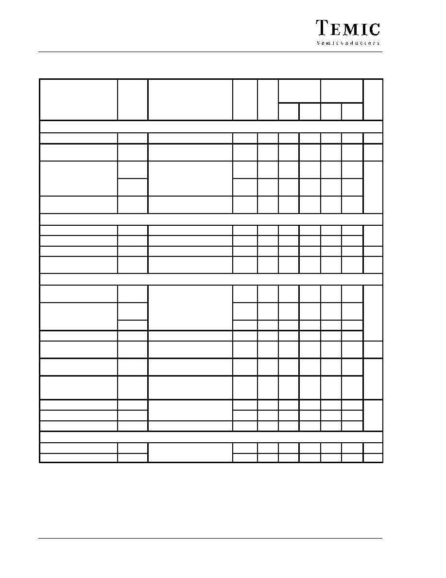
Specifications
a
Conditions Unless
Otherwise Specified
V
15 V V
15 V
A Suffix
≠55 to 125
_C
D Suffix
≠40 to 85
_C
Parameter
Symbol
V+ = 15 V, V≠ = ≠15 V
V
IN
= 3 V, 0.8 V
f
Temp
b
Typ
c
Min
d
Max
d
Min
d
Max
d
Unit
Analog Switch
Analog Signal Range
e
V
ANALOG
Full
V≠
V+
V≠
V+
V
Drain-Source On-Resistance
r
DS(on)
I
S
= ≠10 mA, V
D
=
"8.5 V
V+ = 13.5 V, V≠ = ≠13.5 V
Room
Full
25
50
75
50
75
W
r
DS(on)
Match
Room
3
%
Switch Off Leakage Current
I
S(off)
V+ = 16.5 V, V≠ = ≠16.5 V
V
D =
"15.5 V
Room
Full
0.1
≠1
≠60
1
60
≠1
≠20
1
20
Switch Off Leakage Current
I
D(off)
V
D =
"15.5 V
V
S
=
#15.5 V
Room
Full
0.1
≠1
≠60
1
60
≠1
≠20
1
20
nA
Channel On Leakage Current
I
D(on)
V+ = 16.5 V, V≠ = ≠16.5 V
V
S
= V
D
=
#15.5 V
Room
Full
0.1
≠1
≠60
1
60
≠1
≠20
1
20
Digital Control
Input, High Voltage
V
INH
Full
2.4
2.4
V
Input, Low Voltage
V
INL
Full
0.8
0.8
V
Input Capacitance
C
in
Full
5
pF
Input Current
I
INL
or
I
INH
V
IN
under test = 0.8 V, 3 V
Full
≠1
1
≠1
1
mA
Dynamic Characteristics
Turn-On Time
t
ON
R
L
= 1 k
W, C
L
= 35 pF
Room
Full
48
60
75
60
75
Turn-Off Time
t
OFF1
R
L
= 1 k
W, C
L
= 35 pF
V
S
=
"10 V, V
INH
= 3 V
See Figure 3
Room
Full
30
50
70
50
70
ns
t
OFF2
Room
150
Output Settling Time to 0.1%
t
s
Room
180
Charge Injection
Q
C
L
= 1 nF, V
S
= 0 V
V
gen
= 0 V, R
gen
= 0
W
Room
≠5
pC
OFF Isloation
OIRR
R
L
= 1 k
W, C
L
= 10 pF
f = 100 kHz
Room
85
dB
Crosstalk
(Channel-to-Channel)
X
TALK
Any Other Channel Switches
R
L
= 1 k
W, C
L
= 10 pF
f = 100 kHz
Room
100
dB
Source Off Capacitance
C
S(off)
Room
8
Drain Off Capacitance
C
D(off)
V
S
V
D
= 0 V f = 1 MHz
Room
8
pF
Channel On Capacitance
C
D(on)
V
S
, V
D
= 0 V, f = 1 MHz
Room
30
pF
Drain-to-Source Capacitance
C
DS(off)
Room
0.5
Power Supplies
Positive Supply Current
I+
V+ = 15 V V = 15 V
Room
Full
4.5
10
10
mA
Negative Supply Current
I≠
V+ = 15 V, V≠ = ≠15 V
V
IN
= 0 or 5 V
Room
Full
3.5
≠6
≠6
mA
Power Consumption
c
P
C
Full
240
240
mW
DG201HS
4
Siliconix
E-77071--Rev. E, 01-Sep-97
Specifications
a
for Single Supply
Conditions Unless
Otherwise Specified
V+ = 10.8 V to 16.5 V
A Suffix
≠55 to 125
_C
D Suffix
≠40 to 85
_C
Parameter
Symbol
V+ = 10.8 V to 16.5 V
V≠ = GND = 0 V
V
IN
= 3 V, 0.8 V
f
Temp
b
Typ
c
Min
d
Max
d
Min
d
Max
d
Unit
Analog Switch
Analog Signal Range
e
V
ANALOG
Full
0
V+
0
V+
V
Drain-Source On-Resistance
r
DS(on)
I
S
= ≠10 mA, V
D
= 8.5 V
V+ = 10.8 V
Room
Full
65
90
120
90
120
W
Switch Off Leakage Current
I
S(off)
V+ = 16.5 V, V
S
= 0.5 V, 10 V
V
10 V 0 5 V
Room
Full
0.1
≠1
≠60
1
60
≠1
≠20
1
20
Switch Off Leakage Current
I
D(off)
,
S
,
V
D
= 10 V, 0.5 V
Room
Full
0.1
≠1
≠60
1
60
≠1
≠20
1
20
nA
Channel On Leakage Current
I
D(on)
+
I
S(on)
V+ = 16.5 V, V
D
=
0.5 V, 10 V
Room
Full
0.1
≠1
≠60
1
60
≠1
≠20
1
20
Digital Control
Input, High Voltage
V
INH
Full
2.4
2.4
V
Input, Low Voltage
V
INL
Full
0.8
0.8
V
Input Capacitance
C
in
Full
5
pF
Input Current
I
INL
or
I
INH
V+ = 16.5 V
V
IN
under test = 0.8 V, 3 V
Full
≠1
1
≠1
1
mA
Dynamic Characteristics
Turn-On Time
t
ON
R
1 k
W C
35 F V
2 V
Room
Full
50
70
50
70
Turn-Off Time
t
OFF1
R
L
= 1 k
W, C
L
= 35 pF, V
S
= 2 V
V= 10.8 V, See Figure 2
Room
Full
50
70
50
70
ns
t
OFF2
Room
150
Output Settling Time to 0.1%
t
s
Room
180
Charge Injection
Q
C
L
= 1 nF, V
S
= 0 V
V
gen
= 0 V, R
gen
= 0
W
Room
10
pC
Off Isloation
OIRR
R
L
= 1 k
W, C
L
= 10 pF
f = 100 kHz
Room
85
dB
Crosstalk
(Channel-to-Channel)
X
TALK
Any Other Channel Switches
R
L
= 1 k
W, C
L
= 10 pF
f = 100 kHz
Room
100
dB
Source Off Capacitance
C
S(off)
f = 1 MHz
Room
10
Drain Off Capacitance
C
D(off)
f = 1 MHz
Room
10
pF
Channel On Capacitance
C
D(on)
V
ANALOG
= 0 V
Room
30
Power Supplies
Positive Supply Current
I+
V+ = 15 V V
IN
= 0 or 5 V
Full
10
10
mA
Power Consumption
c
P
C
V+ = 15 V, V
IN
= 0 or 5 V
Full
150
150
mW
Notes:
a.
Refer to PROCESS OPTION FLOWCHART.
b.
Room = 25
_C, Full = as determined by the operating temperature suffix.
c.
Typical values are for DESIGN AID ONLY, not guaranteed nor subject to production testing.
d.
The algebraic convention whereby the most negative value is a minimum and the most positive a maximum, is used in this data sheet.
e.
Guaranteed by design, not subject to production test.
f.
V
IN
= input voltage to perform proper function.

DG201HS
Siliconix
E-77071--Rev. E, 01-Sep-97
5
Typical Characteristics
≠20 ≠16 ≠12 ≠8
≠4
0
4
8
12
16
20
0
10
20
30
40
50
60
70
"5 V
r
DS(on)
vs. V
D
and Power Supply Voltages
V
D
≠ Drain Voltage (V)
"10 V
"15 V
"20 V
0
10
20
30
40
50
≠15
≠10
≠5
0
5
10
15
r
DS(on)
vs. V
D
and Temperature
V
D
≠ Drain Voltage (V)
125_C
85
_C
25
_C
≠55
_C
0
_C
V+ = 15 V
V≠ = ≠15 V
r
DS(on)
≠ Drain-Source On-Resistance (
)
W
r
DS(on)
≠ Drain-Source On-Resistance (
)
W
0
2
4
6
8
10
12
14
16
0
20
40
60
80
100
120
140
160
180
r
DS(on)
vs. V
D
and Single Power Supply Voltages
V
D
≠ Drain Voltage (V)
V+ = 5 V
7 V
10 V
12 V
15 V
≠60 ≠40 ≠20
0
20
40
60
80
100 120 140
10 pA
100 pA
1 nA
10 nA
I
D(on)
Leakage
Leakage Currents vs. Temperature
Temperature (
_C)
I
S(off),
I
D(off)
0
0.5
1
1.5
2
2.5
V
IN
()
V
Input Switching Threshold vs. Supply Voltage
Positive/Negative Supplies (V)
"4 "6 "8 "10 "12 "14 "16 "18 "20
30
35
40
45
50
55
"4 "6 "8 "10 "12 "14 "16 "18 "20
Switching Time vs. Power Supply Voltage
Supply Voltage (V)
Switching T
ime
(ns)
r
DS(on)
≠ Drain-Source On-Resistance (
)
W
t
ON
t
OFF