 | –≠–ª–µ–∫—Ç—Ä–æ–Ω–Ω—ã–π –∫–æ–º–ø–æ–Ω–µ–Ω—Ç: DG418DJ | –°–∫–∞—á–∞—Ç—å:  PDF PDF  ZIP ZIP |

1
Dual-In-Line and SOIC
S
D
NC
V≠
GND
IN
V+
V
L
2
3
4
8
7
6
5
Top View
1
Dual-In-Line and SOIC
D
S
2
S
1
V≠
GND
IN
V+
V
L
2
3
4
8
7
6
5
Top View
DG417
DG419
DG417/418/419
Siliconix
S-52880--Rev. D, 28-Apr-97
1
Precision CMOS Analog Switches
Features
Benefits
Applications
D "15-V Analog Signal Range
D On-Resistance--r
DS(on)
: 20
W
D Fast Switching Action--t
ON
: 100 ns
D Ultra Low Power Requirements--P
D
:35 nW
D TTL and CMOS Compatible
D MiniDIP and SOIC Packaging
D 44-V Supply Max Rating
D Wide Dynamic Range
D Low Signal Errors and Distortion
D Break-Before-Make
Switching Action
D Simple Interfacing
D Reduced Board Space
D Improved Reliability
D Precision Test Equipment
D Precision Instrumentation
D Battery Powered Systems
D Sample-and-Hold Circuits
D Military Radios
D Guidance and Control
Systems
D Hard Disk Drives
Description
The DG417/418/419 monolithic CMOS analog switches
were designed to provide high performance switching of
analog signals. Combining low power, low leakages, high
speed, low on-resistance and small physical size, the
DG417 series is ideally suited for portable and battery
powered industrial and military applications requiring high
performance and efficient use of board space.
To achieve high-voltage ratings and superior switching
performance, the DG417 series is built on Siliconix's high
voltage silicon gate (HVSG) process. Break-before-make is
guaranteed for the DG419, which is an SPDT configuration.
An epitaxial layer prevents latchup.
Each switch conducts equally well in both directions
when on, and blocks up to the power supply level when
off.
The DG417 and DG418 respond to opposite control logic
levels as shown in the Truth Table.
Functional Block Diagram and Pin Configuration
Truth Table
Logic
DG417
DG418
0
ON
OFF
1
OFF
ON
Logic "0" =
v 0.8 V, Logic "1" = w 2.4 V
Truth Table--DG419
Logic
SW
1
SW
2
0
ON
OFF
1
OFF
ON
Logic "0" =
v 0.8 V, Logic "1" = w 2.4 V
Updates to this data sheet may be obtained via facsimile by calling Siliconix FaxBack, 1-408-970-5600. Please request FaxBack document #70051.

DG417/418/419
2
Siliconix
S-52880--Rev. D, 28-Apr-97
Ordering Information
Temp Range
Package
Part Number
DG417/418
8-Pin Plastic MiniDIP
DG417DJ
≠40 to 85
_C
8-Pin Plastic MiniDIP
DG418DJ
≠40 to 85
_C
8-Pin Narrow SOIC
DG417DY
8-Pin Narrow SOIC
DG418DY
≠55 to 125
_C
8-Pin CerDIP
DG417AK, DG417AK/883
≠55 to 125
_C
8-Pin CerDIP
DG418AK, DG418AK/883
DG419
≠40 to 85
_C
8-Pin Plastic MiniDIP
DG419DJ
≠40 to 85
_C
8-Pin Narrow SOIC
DG419DY
≠55 to 125
_C
8-Pin CerDIP
DG419AK, DG419AK/883
Absolute Maximum Ratings
Voltages Referenced to V≠
V+
44 V
. . . . . . . . . . . . . . . . . . . . . . . . . . . . . . . . . . . . . . . . . . . . . . . . . .
GND
25 V
. . . . . . . . . . . . . . . . . . . . . . . . . . . . . . . . . . . . . . . . . . . . . . . . .
V
L
(GND ≠0.3 V) to (V+) + 0.3 V
. . . . . . . . . . . . . . . . . . . . . . . . . . . . . .
Digital Inputs
a
V
S
, V
D
(V≠) ≠2 V to (V+) + 2 V
. . . . . . . . . . . . . . . . . .
or 30 mA, whichever occurs first
Current, (Any Terminal) Continuous
30 mA
. . . . . . . . . . . . . . . . . . . . . .
Current (S or D) Pulsed 1 ms, 10% duty cycle
100 mA
. . . . . . . . . . . . .
Storage Temperature
(AK Suffix)
≠65 to 150
_C
. . . . . . . . . . . . . .
(DJ, DY Suffix)
≠65 to 125
_C
. . . . . . . . . . .
Power Dissipation (Package)
b
8-Pin Plastic MiniDIP
c
400 mW
. . . . . . . . . . . . . . . . . . . . . . . . . . . . . . . .
8-Pin Narrow SOIC
d
400 mW
. . . . . . . . . . . . . . . . . . . . . . . . . . . . . . . . .
8-Pin CerDIP
e
600 mW
. . . . . . . . . . . . . . . . . . . . . . . . . . . . . . . . . . . . . .
Notes:
a.
Signals on S
X
, D
X
, or IN
X
exceeding V+ or V≠ will be clamped by
internal diodes. Limit forward diode current to maximum current
ratings.
b.
All leads welded or soldered to PC Board.
c.
Derate 6 mW/
_C above 75_C
d.
Derate 6.5 mW/
_C above 25_C
e.
Derate 12 mW/
_C above 75_C
Schematic Diagram (Typical Channel)
Figure 1.
Level
Shift/
Drive
V
IN
V
L
S
V+
GND
V-
D
V-
V+

DG417/418/419
Siliconix
S-52880--Rev. D, 28-Apr-97
3
Specifications
a
Test Conditions
Unless Otherwise Specified
A Suffix
≠55 to 125
_C
D Suffix
≠40 to 85
_C
Parameter
Symbol
V+ = 15 V, V≠ = ≠15 V
V
L
= 5 V, V
IN
= 2.4 V, 0.8 V
f
Temp
b
Typ
c
Min
d
Max
d
Min
d
Max
d
Unit
Analog Switch
Analog Signal Range
e
V
ANALOG
Full
≠15
15
≠15
15
V
Drain-Source
On-Resistance
r
DS(on)
I
S
= ≠10 mA, V
D
=
"12.5 V
V+ = 13.5 V, V≠ = ≠13.5 V
Room
Full
20
35
45
35
45
W
I
S(off)
V+
16 5 V V
16 5 V
Room
Full
≠0.1
≠0.25
≠20
0.25
20
≠0.25
≠5
0.25
5
Switch Off
Leakage Current
I
D(off)
V+ = 16.5 V, V≠ = ≠16.5 V
V
D
=
#15.5 V
V
S
=
"15.5 V
DG417
DG418
Room
Full
≠0.1
≠0.25
≠20
0.25
20
≠0.25
≠5
0.25
5
I
D(off)
V
S
"15.5 V
DG419
Room
Full
≠0.1
≠0.75
≠60
0.75
60
≠0.75
≠12
0.75
12
nA
Channel On
L k
C
I
D(on)
V+ = 16.5 V, V≠ = ≠16.5 V
V
V
15 5 V
DG417
DG418
Room
Full
≠0.4
≠0.4
≠40
0.4
40
≠0.4
≠10
0.4
10
Leakage Current
I
D(on)
,
V
S
= V
D
=
"15.5 V
DG419
Room
Full
≠0.4
≠0.75
≠60
0.75
60
≠0.75
≠12
0.75
12
Digital Control
Input Current
V
IN
Low
I
IL
Full
0.005
≠0.5
0.5
≠0.5
0.5
mA
Input Current
V
IN
High
I
IH
Full
0.005
≠0.5
0.5
≠0.5
0.5
mA
Dynamic Characteristics
Turn-On Time
t
ON
R
L
= 300
W
, C
L
= 35 pF
V
S
=
"10 V
DG417
DG418
Room
Full
100
175
250
175
250
Turn-Off Time
t
OFF
S
See Switching Time
Test Circuit
DG417
DG418
Room
Full
60
145
210
145
210
Transition Time
t
TRANS
R
L
= 300
W
, C
L
= 35 pF
V
S1
=
"10 V
V
S2
=
#10 V
DG419
Room
Full
175
250
175
250
ns
Break-Before-Make
Time Delay
t
D
R
L
= 300
W
, C
L
= 35 pF
V
S1
= V
S2
=
"10 V
DG419
Room
13
5
5
Charge Injection
Q
C
L
= 10 nF, V
gen
= 0 V, R
gen
= 0
W
Room
60
pC
Source Off
Capacitance
C
S(off)
f = 1 MHz V
S
= 0 V
Room
8
Drain Off Capacitance
C
D(off)
f = 1 MHz, V
S
= 0 V
DG417
DG418
Room
8
pF
Channel On
Capacitance
C
D(on)
f = 1 MHz, V
S
= 0 V
DG417
DG418
Room
30
p
Capacitance
,
S
DG419
Room
35
Power Supplies
Positive Supply
Current
I+
Room
Full
0.001
1
5
1
5
Negative Supply
Current
I≠
V+ = 16.5 V, V≠ = ≠16.5 V
Room
Full
≠0.001
≠1
≠5
≠1
≠5
A
Logic Supply Current
I
L
V+ = 16.5 V, V≠ = ≠16.5 V
V
IN
= 0 or 5 V
Room
Full
0.001
1
5
1
5
mA
Ground Current
I
GND
Room
Full
≠0.000
1
≠1
≠5
≠1
≠5

DG417/418/419
4
Siliconix
S-52880--Rev. D, 28-Apr-97
Specifications
a
for Unipolar Supplies
Test Conditions
Unless Otherwise Specified
V+
12 V V
0 V
A Suffix
≠55 to 125
_C
D Suffix
≠40 to 85
_C
Parameter
Symbol
V+ = 12 V, V≠ = 0 V
V
L
= 5 V, V
IN
= 2.4 V, 0.8 V
f
Temp
b
Typ
c
Min
d
Max
d
Min
d
Max
d
Unit
Analog Switch
Analog Signal Range
e
V
ANALOG
Full
0
12
0
12
V
Drain-Source
On-Resistance
r
DS(on)
I
S
= ≠10 mA, V
D
= 3.8 V
V+ = 10.8 V
Room
40
W
Dynamic Characteristics
Turn-On Time
t
ON
R
L
= 300
W
, C
L
= 35 pF, V
S
= 8 V
S
S i hi
Ti
T
Ci
i
Room
110
Turn-Off Time
t
OFF
L
,
L
p ,
S
See Switching Time Test Circuit
Room
40
ns
Break-Before-Make
Time Delay
t
D
R
L
= 300
W
, C
L
= 35 pF
DG419
Room
60
ns
Charge Injection
Q
C
L
= 10 nF, V
gen
= 0 V, R
gen
= 0
W
Room
5
pC
Power Supplies
Positive Supply
Current
I+
Room
0.001
Negative Supply
Current
I≠
V+ = 13.2 V, V
L
= 5.25 V
V
IN
= 0 or 5 V
Room
≠0.001
mA
Logic Supply Current
I
L
IN
Room
0.001
Ground Current
I
GND
Room
≠0.001
Notes:
a.
Refer to PROCESS OPTION FLOWCHART.
b.
Room = 25
_C, Full = as determined by the operating temperature suffix.
c.
Typical values are for DESIGN AID ONLY, not guaranteed nor subject to production testing.
d.
The algebraic convention whereby the most negative value is a minimum and the most positive a maximum, is used in this data sheet.
e.
Guaranteed by design, not subject to production test.
f.
V
IN
= input voltage to perform proper function.
DG417/418/419
Siliconix
S-52880--Rev. D, 28-Apr-97
5
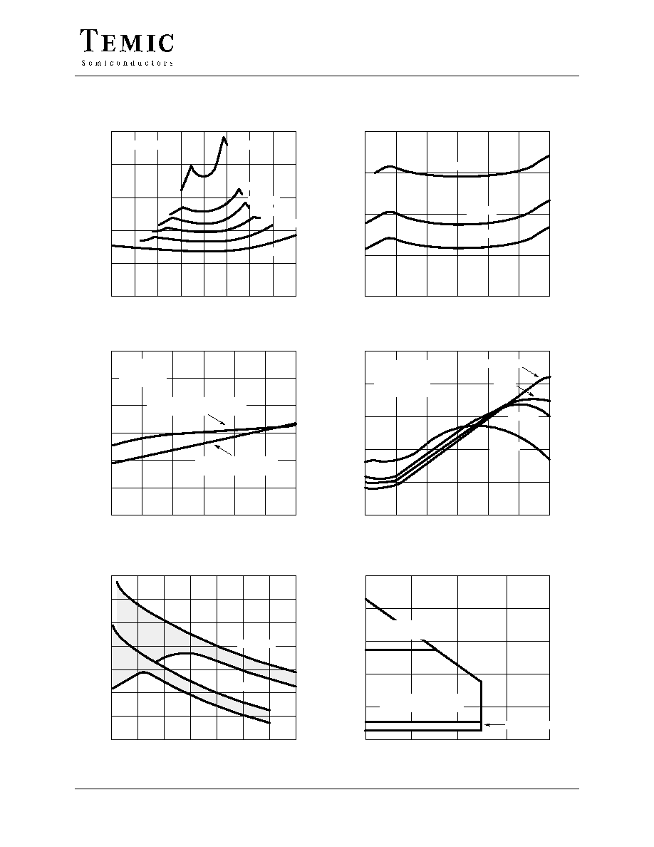
Typical Characteristics
r
DS(on)
r
DS(on)
vs. V
D
and Supply Voltage
50
40
30
0
≠20
≠15
20
20
10
≠10
≠5
5
15
10
0
I
D
= ≠10 mA
"10 V
"15 V
"20 V
"12 V
"8 V
"5 V
r
DS(on)
()
W
r
DS(on)
vs. Temperature
40
30
0
≠15
≠10
15
20
≠5
0
5
10
10
25
_C
≠55
_C
T
A
= 125
_C
Leakage Currents vs. Analog Voltage
I (pA)
30
20
≠30
≠15
≠10
15
10
0
≠5
0
5
10
≠10
≠20
V+ = 15 V
V≠ = ≠15 V
V
L
= 5 V
DG417/418: I
D(off)
, I
S(off)
DG419: I
S(off)
DG417/418: I
D(on)
DG419: I
D(off)
, I
D(on)
Drain Charge Injection
Q (pC)
200
150
100
≠50
≠15
≠10
15
50
0
≠5
0
5
10
100 pF
500 pF
1 nF
V+ = 16.5 V
V≠ = ≠16.5 V
V
L
= 5 V
V
IN
= 0 V
C
L
= 10 nF
(V)
IN
V
Input Switching Threshold vs. Supply Voltages
3.5
3.0
2.5
0
5
10
40
2.0
1.5
1.0
0.5
15
20
25
30
35
(V+)
≠5
≠10
0
≠15
≠10
≠5
0
0
(V≠)
V
L
= 5 V
V
L
= 7 V
Operating Voltage Range
Negative Supply V≠ (V)
V+ (V)
……………………
……………………
……………………
……………………
……………………
……………………
……………………
……………………
……………………
50
40
30
0
0
20
10
≠10
≠20
≠30
≠40
2
42
5 V CMOS
Compatible
TTL Compatible
V
IN
= 0.8 V, 2.4 V
F = Voltages Used for Production Testing
F
F
CMOS Compatible
V
D
≠ Drain Voltage (V)
V
D
or V
S
≠ Drain or Source Voltage (V)
V
D
≠ Drain Voltage (V)
V
S
≠ Source Voltage (V)
()
W