 | –≠–ª–µ–∫—Ç—Ä–æ–Ω–Ω—ã–π –∫–æ–º–ø–æ–Ω–µ–Ω—Ç: DG542 | –°–∫–∞—á–∞—Ç—å:  PDF PDF  ZIP ZIP |

PLCC
14
15
16
17
18
8
7
6
5
4
1
2
3
19
20
11
10
9
13
12
Top View
S
1
GND
V≠
S
2
GND
V+
S
4
GND
GND
S
3
GND
GND
4
D
3
D
3
IN
D
1
IN
1
4
IN
D
2
IN
2
V≠
GND
D
4
S
3
Dual-In-Line
D
3
GND
GND
GND
S
4
GND
S
2
V+
GND
IN
1
IN
3
IN
2
S
1
IN
4
D
1
D
2
1
2
3
4
5
6
7
8
20
19
18
17
16
15
14
13
Top View
9
12
10
11
DG540
DG540
DG540/541/542
Siliconix
S-53694--Rev. E, 28-May-97
1
Wideband/Video "T" Switches
Features
Benefits
Applications
D Wide Bandwidth: 500 MHz
D Low Crosstalk: ≠85 dB
D High Off-Isolation: ≠80 dB @ 5 MHz
D "T" Switch Configuration
D TTL Logic Compatible
D Fast Switching--t
ON
: 45 ns
D Low r
DS(on)
: 30
W
D Flat Frequency Response
D High Color Fidelity
D Low Insertion Loss
D Improved System Performance
D Reduced Board Space
D Reduced Power Consumption
D Improved Data Throughput
D RF and Video Switching
D RGB Switching
D Local and Wide Area Networks
D Video Routing
D Fast Data Acquisition
D ATE
D Radar/FLR Systems
D Video Multiplexing
Description
The DG540/541/542 are high performance monolithic
wideband/video switches designed for switching RF, video
and digital signals. By utilizing a "T" switch configuration
on each channel, these devices achieve exceptionally low
crosstalk and high off-isolation. The crosstalk and
off-isolation of the DG540 are further improved by the
introduction of extra GND pins between signal pins.
To achieve TTL compatibility, low channel capacitances
and fast switching times, the DG540 family is built on the
Siliconix proprietary D/CMOS process. Each switch
conducts equally well in both directions when on.
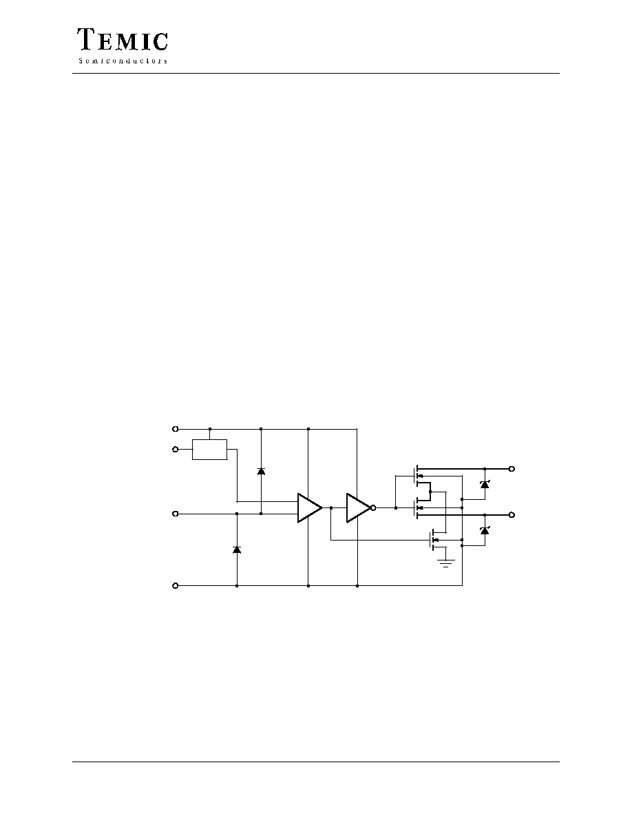
Functional Block Diagrams and Pin Configurations
Truth Table
Logic
Switch
0
OFF
1
ON
Logic "0"
v 0.8 V
Logic "1"
w 2 V
Logic 1
w 2 V
Updates to this data sheet may be obtained via facsimile by calling Siliconix FaxBack, 1-408-970-5600. Please request FaxBack document #70055.

DG540/541/542
2
Siliconix
S-53694--Rev. E, 28-May-97
Functional Block Diagrams and Pin Configurations (Cont'd)
1
2
3
4
5
6
7
8
16
15
14
13
12
11
10
9
Top View
IN
1
IN
2
D
1
D
2
S
1
S
2
V≠
V+
GND
GND
S
4
S
3
D
4
D
3
IN
4
IN
3
DG541
Dual In Line and SOIC
DG542
1
2
3
4
5
6
7
8
16
15
14
13
12
11
10
9
Top View
IN
1
IN
2
D
1
D
2
GND
GND
S
1
S
2
V≠
V+
S
4
S
3
GND
GND
D
4
D
3
Dual-In-Line and SOIC
Truth Table - DG541
Logic
Switch
0
OFF
1
ON
Logic "0"
v 0.8 V
Logic "1"
w 2 V
Truth Table - DG542
Logic
SW
1
, SW
2
SW
3
, SW
4
0
OFF
ON
1
ON
OFF
Logic "0"
v 0.8 V
Logic "1"
w 2 V
Ordering Information
Temp Range
Package
Part Number
DG540
≠40to 85
_C
20-Pin Plastic DIP
DG540DJ
≠40 to 85
_C
20-Pin PLCC
DG540DN
≠55 to 125
_C
20-Pin Sidebraze
DG540AP
≠55 to 125
_C
20-Pin Sidebraze
DG540AP/883
DG541
≠40 to 85
_C
16-Pin Plastic DIP
DG541DJ
≠40 to 85
_C
16-Pin Narrow SOIC
DG541DY
≠55 to 125
_C
16-Pin Sidebraze
DG541AP
≠55 to 125
_C
16-Pin Sidebraze
DG541AP/883
DG542
≠40 to 85
_C
16-Pin Plastic DIP
DG542DJ
≠40 to 85
_C
16-Pin Narrow SOIC
DG542DY
≠55 to 125
_C
16-Pin Sidebraze
DG542AP
≠55 to 125
_C
16-Pin Sidebraze
DG542AP/883
DG540/541/542
Siliconix
S-53694--Rev. E, 28-May-97
3
Absolute Maximum Ratings
V+ to V≠
≠0.3 V to 21 V
. . . . . . . . . . . . . . . . . . . . . . . . . . . . . . . . . . . . .
V+ to GND
≠0.3 V to 21 V
. . . . . . . . . . . . . . . . . . . . . . . . . . . . . . . . . . . .
V≠ to GND
≠19 V to +0.3 V
. . . . . . . . . . . . . . . . . . . . . . . . . . . . . . . . . . .
Digital Inputs
(V≠) ≠0.3 V to (V+) +0.3 V
. . . . . . . . . . . . . . . . . . . . . . . .
or 20 mA, whichever occurs first
V
S
, V
D
(V≠) ≠0.3 V to (V≠) +14 V
. . . . . . . . . . . . . . . . . . . . . . . . . . . . .
or 20 mA, whichever occurs first
Continuous Current (Any Terminal)
20 mA
. . . . . . . . . . . . . . . . . . . . . .
Current, S or D (Pulsed 1 ms, 10% duty cycle max)
40 mA
. . . . . . . . . .
Storage Temperature
(AP Suffix)
≠65 to 150
_C
. . . . . . . . . . . . . .
(DJ, DN, DY Suffixes)
≠65 to 125
_C
. . . . .
Power Dissipation (Package)a
16-Pin Plastic DIP
b
470 mW
. . . . . . . . . . . . . . . . . . . . . . . . . . . . . . . . . .
20-Pin Plastic DIP
c
800 mW
. . . . . . . . . . . . . . . . . . . . . . . . . . . . . . . . . .
16-Pin Narrow Body SOIC
d
640 mW
. . . . . . . . . . . . . . . . . . . . . . . . . . .
20-Pin PLCC
d
800 mW
. . . . . . . . . . . . . . . . . . . . . . . . . . . . . . . . . . . . . .
16-, 20-Pin Sidebraze DIP
e
900 mW
. . . . . . . . . . . . . . . . . . . . . . . . . . . .
Notes:
a.
All leads welded or soldered to PC Board.
b.
Derate 6.5 mW/
_C above 25_C
c.
Derate 7 mW/
_C above 25_C
d.
Derate 10 mW/
_C above 75_C
e.
Derate 12 mW/
_C above 75_C
Schematic Diagram (Typical Channel)
Figure 1.
V+
IN
V≠
GND
≠
+
S
D
V
REF
DG540/541/542
4
Siliconix
S-53694--Rev. E, 28-May-97
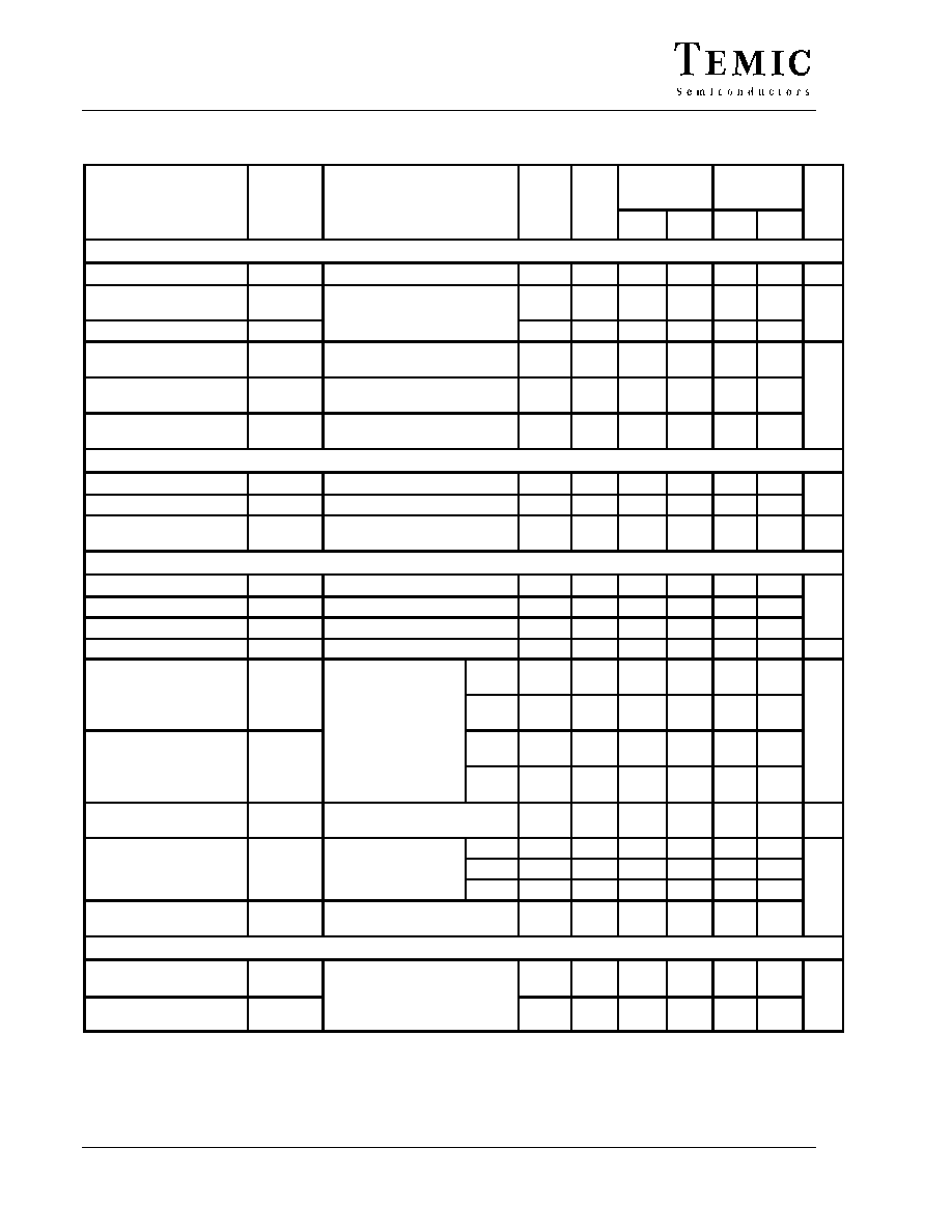
Specifications
a
Test Conditions
Unless Specified
V+
15 V V
3 V
A Suffix
≠55 to 125
_C
D Suffixes
≠40 to 85
_C
Parameter
Symbol
V+ = 15 V, V≠ = ≠3 V
V
INH
= 2 V, V
INL
= 0.8 V
f
Temp
b
Typ
c
Min
d
Max
d
Min
d
Max
d
Unit
Analog Switch
Analog Signal Range
V
ANALOG
V≠ = ≠5 V, V+ = 12 V
Full
≠5
5
≠5
5
V
Drain-Source
On-Resistance
r
DS(on)
I
S
= ≠10 mA, V
D
= 0 V
Room
Full
30
60
100
60
75
W
r
DS(on)
Match
Dr
DS(on)
S
,
D
Room
2
6
6
Source Off
Leakage Current
I
S(off)
V
S
= 0 V, V
D
= 10 V
Room
Full
≠0.05
≠10
≠500
10
500
≠10
≠100
10
100
Drain Off
Leakage Current
I
D(off)
V
S
= 10 V, V
D
= 0 V
Room
Full
≠0.05
≠10
≠500
10
500
≠10
≠100
10
100
nA
Channel On
Leakage Current
I
D(on)
V
S
= V
D
= 0 V
Room
Full
≠0.05
≠10
≠1000
10
1000
≠10
≠100
10
100
Digital Control
Input Voltage High
V
INH
Full
2
2
V
Input Voltage Low
V
INL
Full
0.8
0.8
V
Input Current
I
IN
V
IN
= GND or V+
Room
Full
0.05
≠1
≠20
1
20
≠1
≠20
1
20
mA
Dynamic Characteristics
On State Input Capacitance
e
C
S(on)
V
S
= V
D
= 0 V
Room
14
20
20
Off State Input Capacitance
e
C
S(off)
V
S
= 0 V
Room
2
4
4
pF
Off State Output Capacitance
e
C
D(off)
V
D
= 0 V
Room
2
4
4
Bandwidth
BW
R
L
= 50
W, See Figure 5
Room
500
MHz
Turn On Time
t
ON
W
DG540
DG541
Room
Full
45
70
130
70
130
Turn On Time
t
ON
R
L
= 1 k
W
C
L
= 35 pF
DG542
Room
Full
55
100
160
100
160
ns
Turn Off Time
t
OFF
L
p
50% to 90%
See Figure 2
DG540
DG541
Room
Full
20
50
85
50
85
ns
Turn Off Time
t
OFF
DG542
Room
Full
25
60
85
60
85
Charge Injection
Q
C
L
= 1000 pF, V
S
= 0 V
See Figure 3
Room
≠25
pC
R
IN
= 75
W
R
75
W
DG540
Room
≠80
Off Isolation
OIRR
R
L
= 75
W
f = 5 MHz
DG541
Room
≠60
f = 5 MHz
See Figure 4
DG542
Room
≠75
dB
All Hostile Crosstalk
X
TALK(AH)
R
IN
= 10
W, R
L
= 75
W
f = 5 MHz, See Figure 6
Room
≠85
Power Supplies
Positive Supply Current
I+
All Channels On or Off
Room
Full
3.5
6
9
6
9
mA
Negative Supply Current
I≠
All Channels On or Off
Room
Full
≠3.2
≠6
≠9
≠6
≠9
mA
Notes:
a.
Refer to PROCESS OPTION FLOWCHART.
b.
Room = 25
_C, Full = as determined by the operating temperature suffix.
c.
Typical values are for DESIGN AID ONLY, not guaranteed nor subject to production testing.
d.
The algebraic convention whereby the most negative value is a minimum and the most positive a maximum, is used in this data sheet.
e.
Guaranteed by design, not subject to production test.
f.
V
IN
= input voltage to perform proper function.
DG540/541/542
Siliconix
S-53694--Rev. E, 28-May-97
5
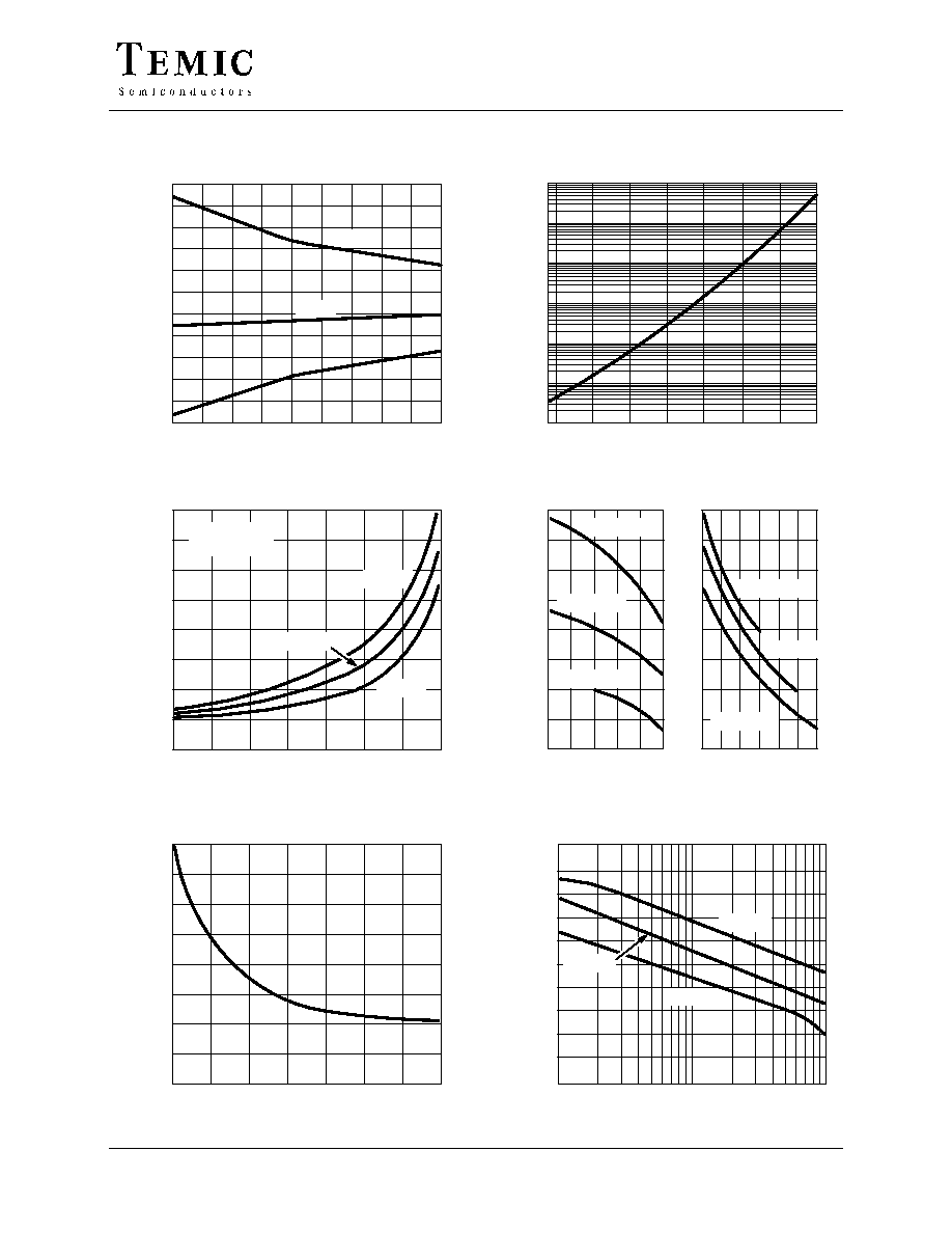
Typical Characteristics
Supply Curent vs. Temperature
I
D(off)
, I
S(off)
vs. Temperature
r
DS(on)
vs. Drain Voltage
V+ Constant
V≠ Constant
Temperature (
_C)
Temperature (
_C)
V
D
≠ Drain Voltage (V)
V≠ ≠ Negative Supply (V)
V+ ≠ Positive Supply (V)
I (mA)
6
5
4
3
2
1
0
≠1
≠2
≠3
≠4
≠5
≠55
≠35 ≠15
5
25
45
65
85
105 125
I
GND
0
≠55
125
100 nA
10 nA
1 nA
100 pA
10 pA
1 pA
0.1 pA
≠25
25
50
75
100
160
140
120
100
80
60
40
20
0
≠3
≠1
1
3
5
7
9
11
V+ = 15 V
V≠ = ≠3 V
125
_C
≠55
_C
42
40
38
36
34
32
30
20
18
10 11 12 13 14 15 16
42
40
38
36
34
32
30
20
18
≠5 ≠4 ≠3
≠2 ≠1
0
V+ = 12 V
V+ = 15 V
V≠ = ≠5 V
V≠ = ≠1 V
V+ = 10 V
I≠
I+
≠ Leakage
I
, I
S(of
f)
D(of
f)
r
DS(on)
≠ Drain-Source On-Resistance (
r
DS(on)
≠ Drain-Source On-Resistance (
25
_C
V≠ = ≠3 V
)
W
)
W
On Capacitance
Off Isolation
V
D
≠ Drain Voltage (V)
f ≠ Frequency (MHz)
C (pF)
ISO (dB)
22
20
18
16
14
12
10
8
6
0
2
4
6
8
10
12
14
1
10
100
≠110
≠100
≠90
≠80
≠70
≠60
≠50
≠40
≠30
≠20
≠10
DG541
DG540
DG542