 | –≠–ª–µ–∫—Ç—Ä–æ–Ω–Ω—ã–π –∫–æ–º–ø–æ–Ω–µ–Ω—Ç: E5530 | –°–∫–∞—á–∞—Ç—å:  PDF PDF  ZIP ZIP |

e5530
Rev. A3, 17-Sep-98
1 (5)
128-Bit IDIC
Æ
for Radio Frequency Identification
Description
The e5530 is part of a closed coupled identification
system. It receives power from an RF transmitter which
is coupled inductively to the IDIC
Æ
. The frequency is
typically 100 to 450 kHz. Receiving RF, the IDIC
Æ
responds with a data stream by damping the incoming RF
via an internal load. This damping-in-turn can be detected
by the interrogator. The identifying data are stored in a
128 bit PROM on the e5530, realized as an array of laser-
programmable fuses. The logic block diagram for the
e5530 is shown in figure 2. The data are output bit-
serially as a code of length 128, 96, 64 or 32 bits. The
chips are factory-programmed with a unique code.
Features
D Low power, low voltage CMOS
D Rectifier, voltage limiter, clock extraction
on-chip (no battery)
D Small size
D Factory laser programmable ROM
D Operating temperature range ≠40 to +125
∞
C
D Radio Frequency (RF): 100 to 450 kHz
D Transmission options
Code length: 128, 96, 64, 32 bits
Bitrate [bit/s]:
RF/8,RF/16, RF/32, RF/40,
RF/50, RF/64, RF/80, RF/100,
RF/128, RF/256
Modulation:
FSK, PSK, BIPH, Manchester
BIPH-FSK
Application
RF transmitter
and
interrogator
e5530
RF
95 10318
IDIC
Æ
Figure 1. Application
R7
R6
R5
R4
R3
R2
R1
R0
Row decoder
C15
C14
C13
C12
C1
1
C10
C9
C8
C7
C6
C5
C4
C3
C2
C1
C0
Column decoder
A2
A1
A0
A6
A5
A4
A3
Counter
Modulator
FSK
PSK
BIPH
Manchester
Bitrate
Data
Load
Clock
extractor
Rectifier
Mod
Clk
Analog front end
Coil
Coil
V
DD
V
SS
128 bit PROM
95 10155
Figure 2. Block diagram
IDIC
Æ
stands for IDentification Integrated Circuit and is a trademark of TEMIC.

e5530
Rev. A3, 17-Sep-98
2 (5)
Ordering Information
Extended Type Number
Package
Checksum
Header
IP Code
SPQ
(Minimum
Volume)
Minimum
Order Volume
e5530H-232-DOW
e5530H-232-DIT
e5530H-232-S8
DOW
DIT
SO8
no
checksum
E6
fixed and
unique code
10 kpcs
10 kpcs
1120
10 kpcs
10 kpcs
1120
e5530H-zzz-DOW *
e5530H-zzz-DIT *
e5530H-zzz-S8 *
DOW
DIT
SO8
defined by customer
> 600 kpcs p.a.
> 600 kpcs p.a.
> 400 kpcs p.a.
*
1) Definition of customized part number basing on orders for first year volume (300 kpcs)
2) Definition of header, ID code, checksum etc. according to customers data base
3) 8.000 US$ initial cost for metal mask
4) Lead time 5 month
5) Low volume customized application can be covered by TK5550F≠PP programming.
With identical features of TK5530H≠zzz≠pPP possible
Chip Dimensions
e5530
1.17 mm
1.62 mm
13368
Coil 1
Coil 2
0.447 mm
0.175 mm
Pad: 150
m x 150 m (Metal: 99% Al, 1% Si)
Padwindow: 138
m x 138 m
Figure 3. Chip size
Pads
Name
Pad Window
Function
¡¡¡¡
¡¡¡¡
Coil1
¡¡¡¡¡¡
¡¡¡¡¡¡
138
138 mm
2
¡¡¡¡¡¡¡¡
¡¡¡¡¡¡¡¡
1st coil pad
¡¡¡¡
¡¡¡¡
Coil2
¡¡¡¡¡¡
¡¡¡¡¡¡
138
138 mm
2
¡¡¡¡¡¡¡¡
¡¡¡¡¡¡¡¡
2nd coil pad
Coil 1
Coil 2
1
2
3
4
8
7
6
5
13367
e5530
Note:
Pins 2 to 7 have to be open. They are
not specified for applications
Figure 4. Pinning SO8
Functional Description
Read Operation
Once the IC detects the incoming RF, the IC repetively
reads out the code data as long as the RF signal is applied.
The transition from the last bit to bit 1 of the next
sequence occurs without interruption. Data is transmitted
by alternating damping of the incoming RF via a load.
Different kinds of modulation and bitrates are optionally
available.
Rectifier
For internal power supply, an on-chip bridge rectifier is
used which consists of two diodes and two n-channel
transistors. A Zener diode, which protects the circuit
against overvoltage on the coil inputs, and a smoothing
capacitor for the internal supply are also provided.
Damping Load
Incoming RF will be damped by the power consumption
of the IC itself and by an internal load, which is controlled
by the modulator. The loads are p-channel transistors
connected between V
DD
and the coil inputs. The layout
includes metal mask options for the load circuit:
single-side, double-side and alternate-side modulation.
Modulator
One of four methods of modulation can be selected by
fuses. The timing diagram is shown in figure 5.
FSK
Logical "1" and "0" are distinguished via different
frequencies of damping. The frequency for "1" is the RF
divided by 10, a "0" divides by 8.

e5530
Rev. A3, 17-Sep-98
3 (5)
PSK
A logical "1" causes (at the end of the bit period) a 180
∞
phase shift on the carrier frequency, while a logical "0"
causes no phase shift. The carrier frequency is RF/2.
BIPH
Logical "1" produces a signal which is the same as the bit-
clock and a logical "0" produces a signal of twice the
bitclock period.
Manchester
A logical "1" causes a positive edge in the middle of a bit
period, while a logical "0" causes negative edge.
A combination of BIPH- and FSK-modulation is also
optionally available. The available combinations be-
tween the modulation types and the bitrates are shown in
table "Transmission Options".
DataClk
Data
PSK
FSK
Biph
Man
1
1
1
1
0
0
0
95 10278
Figure 5. Timing diagram for modulation options
Absolute Maximum Ratings
Parameters
Symbol
Value
Unit
Maximum current into Coil1 and Coil2
I
coil
10
mA
Maximum power dissipation (dice)
P
tot
100
mW
*
Maximum ambient air temperature with voltage applied
T
amb
≠40 to +125
∞
C
Storage temperature
T
stg
≠65 to +150
∞
C
*
Free-air condition. Time of application: 1 s
Stresses above those listed under `Absolute Maximum Ratings' may cause permanent damage to the device.
Functional operation of the device at these conditions is not imlied.
e5530
Rev. A3, 17-Sep-98
4 (5)
Operating Characteristics
T
amb
= 25
∞
C, reference terminal is V
DD
, operating voltage V
DD
≠ V
SS
= 3 V dc, unless otherwise specified
Parameters
Test Conditions / Pins
Symbol
Min.
Typ. *
Max.
Unit
Operating voltage
Condition for logic test
V
SS
≠1.5
≠5.0
V
Operating temperature
T
amb
≠40
125
∞
C
Input frequency (RF)
f
CLK
100
450
kHz
Operating current
f
CLK
= 125 kHz,
V
SS
= ≠2 V
I
CC
3
mA
Clamp voltage
I = 4 mA
V
CL
6.7
10
V
*
Typical parameters represent the statistical mean values
Transmission Options
Modulation
Carrier Frequency (CF)
Bitrate [bit/s]
FSK
RF/8, RF/10
RF/32, RF/40, RF/50, RF/64, RF/80,
RF/100, RF/128
PSK
RF/2
CF/4, 8, 16, 32
BIPH
RF/8, RF/16, RF/32, RF/64, RF/100,
RF/128
Manchester
RF/8, RF/16, RF/32, RF/64, RF/100,
RF/128
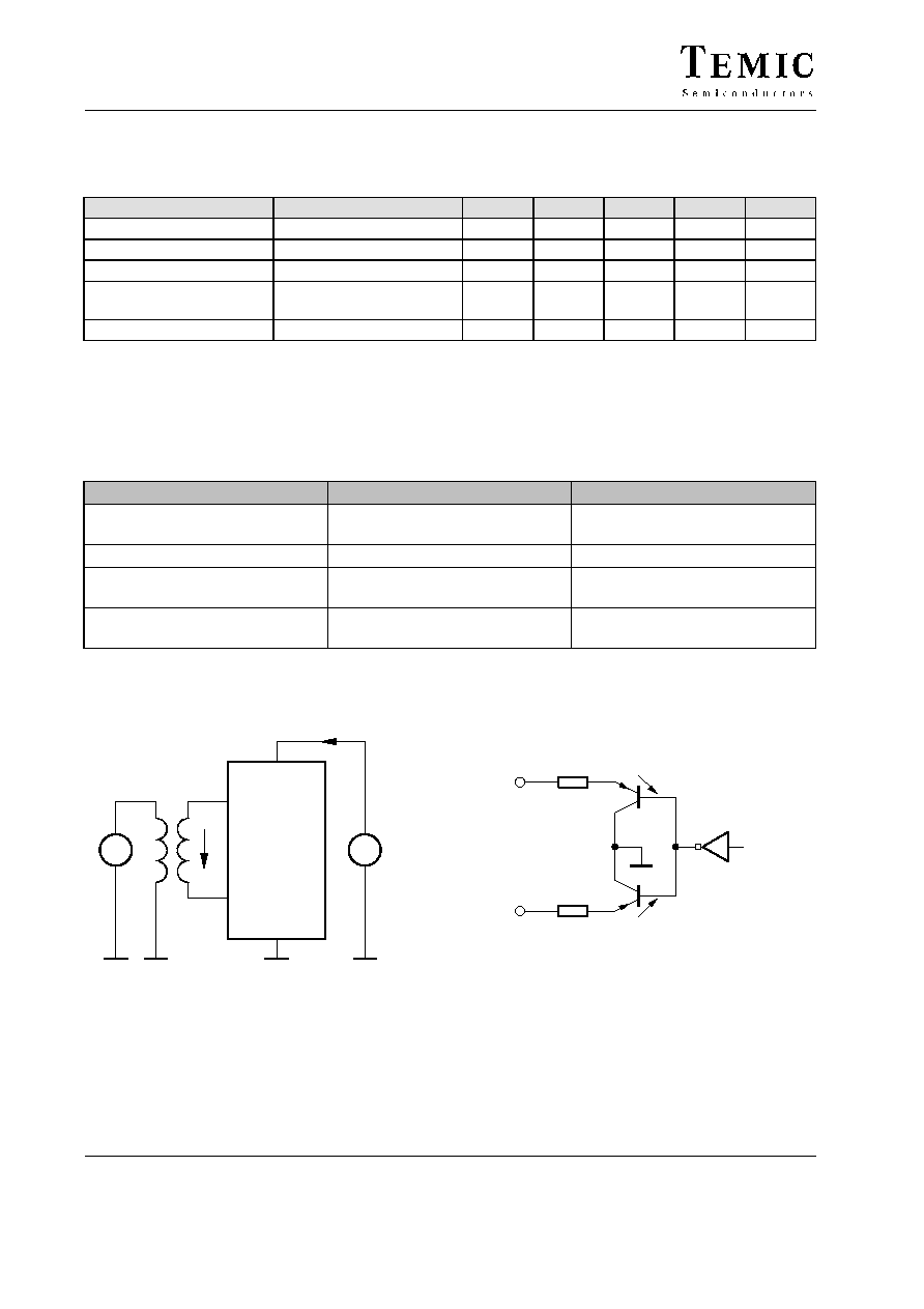
~
Coil 1
Coil 2
V
DD
V
SS
=
2 V
I
DD
V
pp Coil
1.5 V
96 12303
Figure 6. Measurement setup for I
DD
Coil 1
Mod
96 12304
Coil 2
100
W
~ 2 V
~ 2 V
100
W
Figure 7. Simplified damping circuit

e5530
Rev. A3, 17-Sep-98
5 (5)
Application Example
I
125 kHz
Coil1 (Pin 8)
Coil2 (Pin 1)
2.2 nF
To read
amplifier
e5530
390 pF
4.05 mH
From
oscillator
Energy
Data
f
res
+
1
2
p LC
+ 125 kHz
13369
AC
740
mH
Input capacitance
5 pF static, 4 pF dynamic
(SO8)
Figure 8. Typical application circuit
Package Information
13034
technical drawings
according to DIN
specifications
Package SO8
Dimensions in mm
5.00
4.85
0.4
1.27
3.81
1.4
0.25
0.10
5.2
4.8
3.7
3.8
6.15
5.85
0.2
8
5
1
4
We reserve the right to make changes to improve technical design and may do so without further notice.
Parameters can vary in different applications. All operating parameters must be validated for each customer
application by the customer. Should the buyer use TEMIC products for any unintended or unauthorized
application, the buyer shall indemnify TEMIC against all claims, costs, damages, and expenses, arising out of,
directly or indirectly, any claim of personal damage, injury or death associated with such unintended or
unauthorized use.
TEMIC Semiconductor GmbH, P.O.B. 3535, D-74025 Heilbronn, Germany
Telephone: 49 ( 0 ) 7131 67 2594, Fax number: 49 ( 0 ) 7131 67 2423