
SUP/SUB75N06-08
Siliconix
S-47969--Rev. D, 08-Jul-96
1
N-Channel Enhancement-Mode Transistors
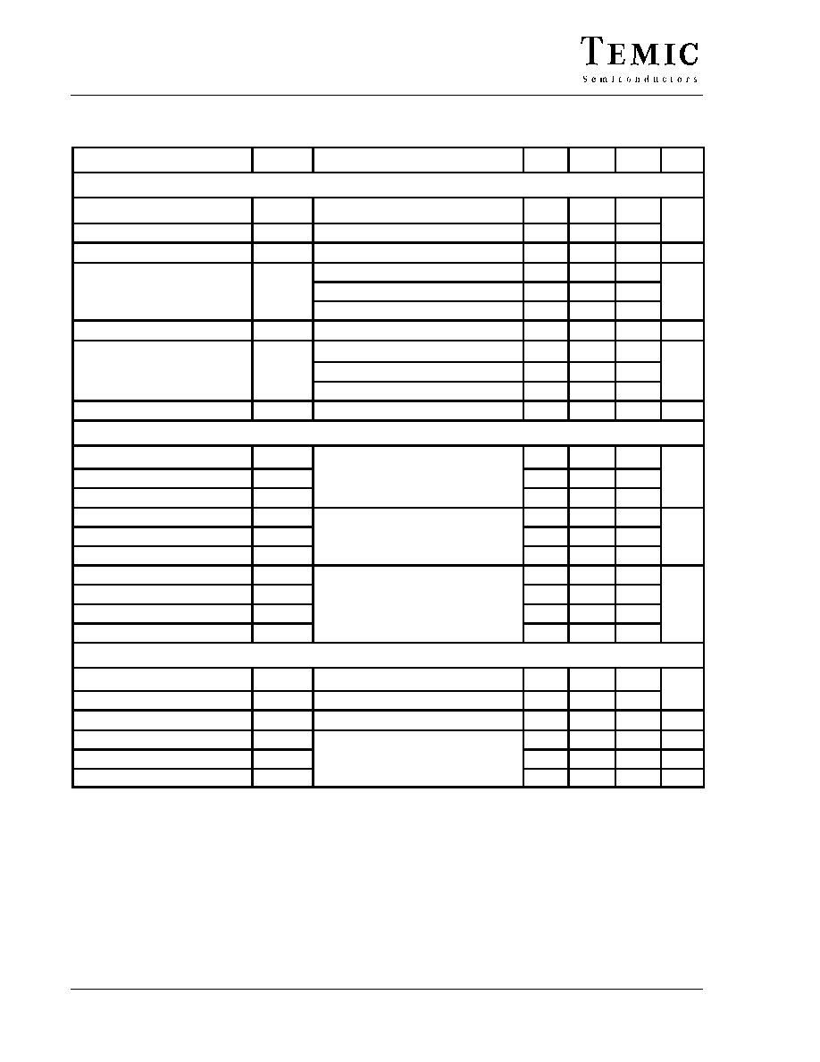
Product Summary
V
(BR)DSS
(V)
r
DS(on)
(
W)
I
D
(A)
60
0.008
75
a
D
G
S
N-Channel MOSFET
TO-220AB
Top View
G D S
DRAIN connected to TAB
TO-263
S
D
G
Top View
SUP75N06-08
SUB75N06-08
Absolute Maximum Ratings (
T
C
= 25
_C Unless Otherwise Noted
)
Parameter
Symbol
Limit
Unit
Gate-Source Voltage
V
GS
"20
V
Continuous Drain Current
(T
175
_C)
T
C
= 25
_C
I
D
75
a
(T
J
= 175
_C)
T
C
= 125
_C
I
D
55
A
Pulsed Drain Current
I
DM
240
A
Avalanche Current
I
AR
60
Repetitive Avalanche Energy
b
L = 0.1 mH
E
AR
280
mJ
Power Dissipation
T
C
= 25
_C (TO-220AB and TO-263)
P
D
187
c
W
Power Dissipation
T
A
= 25
_C (TO-263)
d
P
D
3.7
W
Operating Junction and Storage Temperature Range
T
J
, T
stg
≠55 to 175
_C
Thermal Resistance Ratings
Parameter
Symbol
Limit
Unit
Junction to Ambient
PCB Mount (TO-263)
d
R
thJA
40
Junction-to-Ambient
Free Air (TO-220AB)
R
thJA
62.5
_C/W
Junction-to-Case
R
thJC
0.8
Notes
a.
Package limited.
b.
Duty cycle
v 1%.
c.
See SOA curve for voltage derating.
d.
When mounted on 1" square PCB (FR-4 material).
Updates to this data sheet may be obtained via facsimile by calling Siliconix FaxBack, 1-408-970-5600. Please request FaxBack document # 70283.
A SPICE Model data sheet is available for this product (FaxBack document #70527).
SUP/SUB75N06-08
2
Siliconix
S-47969--Rev. D, 08-Jul-96
Specifications (T
J
= 25
_C Unless Otherwise Noted)
Parameter
Symbol
Test Condition
Min
Typ
Max
Unit
Static
Drain Source Breakdown Voltage
V
(BR)DSS
V
GS
= 0 V, I
D
= 250
mA
60
V
Gate Threshold Voltage
V
GS(th)
V
DS
= V
GS
, I
D
= 250
mA
2.0
3.0
4.0
V
Gate-Body Leakage
I
GSS
V
DS
= 0 V, V
GS
=
"20 V
"100
nA
V
DS
= 60 V, V
GS
= 0 V
1
Zero Gate Voltage Drain Current
I
DSS
V
DS
= 60 V
,
V
GS
= 0 V, T
J
= 125
_C
50
mA
V
DS
= 60 V, V
GS
= 0 V, T
J
= 175
_C
150
On-State Drain Current
b
I
D(on)
V
DS
= 5 V, V
GS
= 10 V
120
A
b
V
GS
= 10 V, I
D
= 30 A
0.007
0.008
W
Drain-Source On-State Resistance
b
r
DS(on)
V
GS
= 10 V, I
D
= 30 A, T
J
= 125
_C
0.012
W
V
GS
= 10 V, I
D
= 30 A, T
J
= 175
_C
0.016
Forward Transconductance
b
g
fs
V
DS
= 15 V, I
D
= 30 A
30
S
Dynamic
a
Input Capacitance
C
iss
4800
Output Capacitance
C
oss
V
GS
= 0 V, V
DS
= 25 V, f = 1 MHz
910
pF
Reverse Transfer Capacitance
C
rss
270
Total Gate Charge
c
Q
g
85
120
Gate-Source Charge
c
Q
gs
V
DS
= 30 V
,
V
GS
= 10 V, I
D
= 75 A
28
nC
Gate-Drain Charge
c
Q
gd
26
Turn-On Delay Time
c
t
d(on)
W
20
40
Rise Time
c
t
r
V
DD
= 30 V, R
L
= 0.47
W
I
75 A V
10 V R
2 5
W
95
200
ns
Turn-Off Delay Time
c
t
d(off)
DD
,
L
I
D
^ 75 A, V
GEN
= 10 V, R
G
= 2.5
W
65
120
ns
Fall Time
c
t
f
20
60
Source Drain Diode Ratings and Characteristics (T
C
= 25_C)
a
Continuous Current
I
S
75
A
Pulsed Current
I
SM
240
A
Forward Voltage
b
V
SD
I
F
= 75 A , V
GS
= 0 V
1.0
1.3
V
Reverse Recovery Time
t
rr
67
120
ns
Peak Reverse Recovery Current
I
RM(REC)
I
F
= 75 A, di/dt = 100 A/
ms
6
8
A
Reverse Recovery Charge
Q
rr
0.2
0.48
mC
Notes
a.
Guaranteed by design, not subject to production testing.
b.
Pulse test: pulse width
v
300
msec, duty cycle v
2%.
c.
Independent of operating temperature.
SUP/SUB75N06-08
Siliconix
S-47969--Rev. D, 08-Jul-96
3
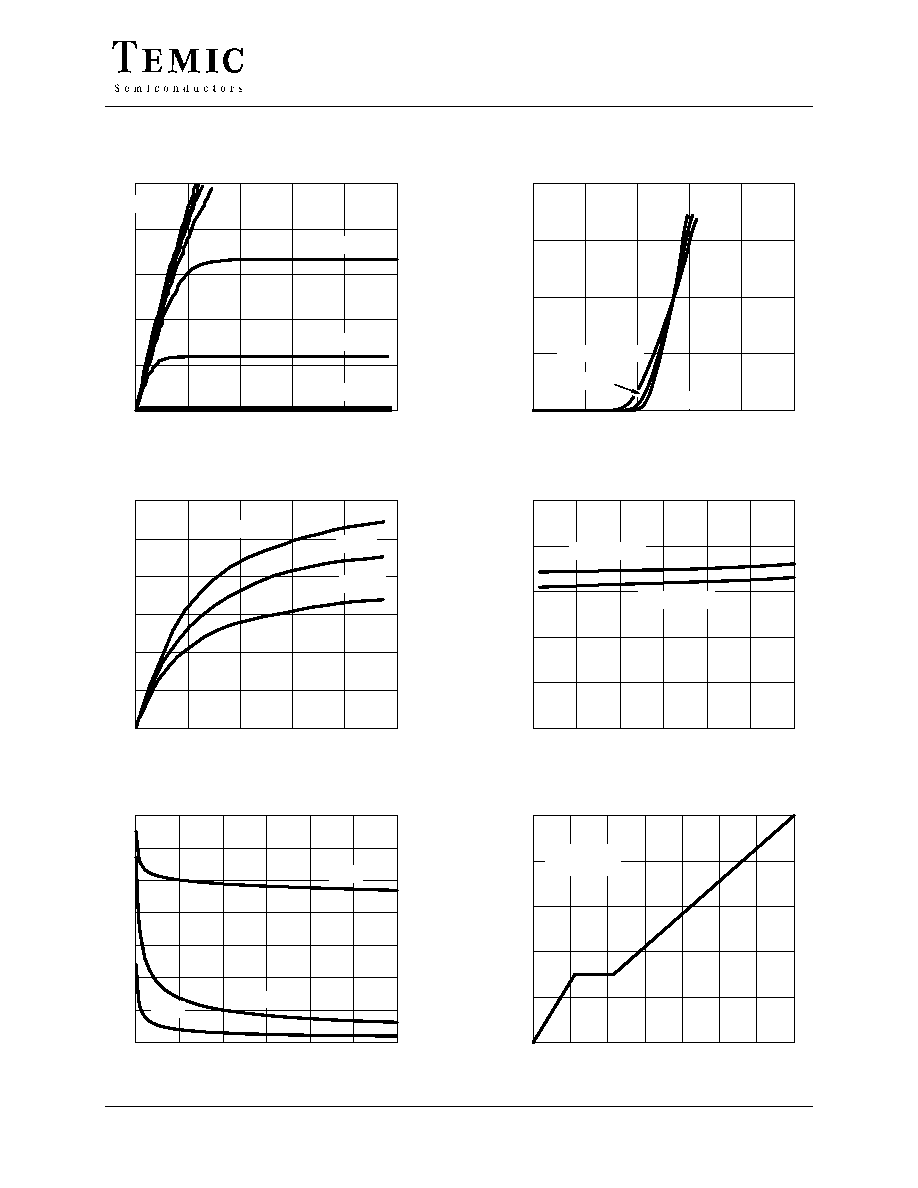
Typical Characteristics (25
_C Unless Otherwise Noted)
Output Characteristics
Transfer Characteristics
Capacitance
Gate Charge
Transconductance
On-Resistance vs. Drain Current
V
DS
≠ Drain-to-Source Voltage (V)
≠ Drain Current (A)
I
D
V
GS
≠ Gate-to-Source Voltage (V)
≠ Drain Current (A)
I
D
≠ Gate-to-Source
V
oltage (V)
≠ On-Resistance (
Q
g
≠ Total Gate Charge (nC)
I
D
≠ Drain Current (A)
V
DS
≠ Drain-to-Source Voltage (V)
C ≠ Capacitance (pF)
r
DS(on)
W
)
V
GS
V
GS
≠ Gate-to-Source Voltage (V)
≠ T
ransconductance
(S)
g
fs
0
50
100
150
200
250
0
2
4
6
8
10
0
1000
2000
3000
4000
5000
6000
7000
0
10
20
30
40
50
60
0
4
8
12
16
20
0
25
50
75
100
125
150
175
0
20
40
60
80
100
120
0
20
40
60
80
100
0
0.002
0.004
0.006
0.008
0.010
0
20
40
60
80
100
120
0
50
100
150
200
0
2
4
6
8
10
25
_C
≠55
_C
5 V
T
C
= 125
_C
V
DS
= 30 V
I
D
= 75 A
V
GS
= 10, 9, 8 V
6 V
7 V
V
GS
= 10 V
V
GS
= 20 V
C
iss
C
oss
C
rss
T
C
= ≠55
_C
25
_C
125
_C
4 V
SUP/SUB75N06-08
4
Siliconix
S-47969--Rev. D, 08-Jul-96
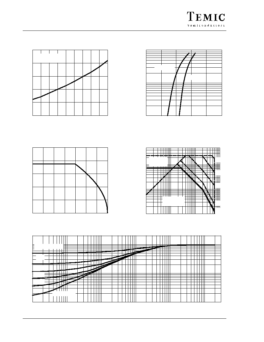
Typical Characteristics (25
_C Unless Otherwise Noted)
On-Resistance vs. Junction Temperature
Source-Drain Diode Forward Voltage
(Normalized)
≠ On-Resistance (
T
J
≠ Junction Temperature (
_C)
V
SD
≠ Source-to-Drain Voltage (V)
r
DS(on)
W
)
≠ Source Current (A)
I
S
0
0.5
1.0
1.5
2.0
2.5
≠50
≠25
0
25
50
75
100
125
150
175
100
10
1
0.3
0.6
0.9
1.2
1.5
V
GS
= 10 V
I
D
= 30 A
T
J
= 25
_C
T
J
= 150
_C
Thermal Ratings
Normalized Thermal Transient Impedance, Junction-to-Case
Square Wave Pulse Duration (sec)
2
1
0.1
0.01
10
≠5
10
≠4
10
≠3
10
≠2
10
≠1
1
Normalized Ef
fective
T
ransient
Thermal Impedance
3
Safe Operating Area
Maximum Avalanche and Drain Current
vs. Case Temperature
T
C
≠ Case Temperature (
_C)
V
DS
≠ Drain-to-Source Voltage (V)
≠ Drain Current (A)
I
D
≠ Drain Current (A)
I
D
100
500
10
1
0
20
40
60
80
100
0
25
50
75
100
125
150
175
0.2
0.1
0.05
0.02
Single Pulse
Duty Cycle = 0.5
10 ms
100 ms
1 ms
10 ms
100 ms
dc
T
C
= 25
_C
Single Pulse
Limited
by r
DS(on)
0.1
1
10
100