 | –≠–ª–µ–∫—Ç—Ä–æ–Ω–Ω—ã–π –∫–æ–º–ø–æ–Ω–µ–Ω—Ç: TDA4455 | –°–∫–∞—á–∞—Ç—å:  PDF PDF  ZIP ZIP |

TELEFUNKEN Semiconductors
TDA4455
Preliminary Information
Rev. A1: 08.05.1995
1 (12)
Multistandard VIF Amplifier and PLL Demodulator
Application
Monolithic integrated circuit for vision IF signal processing in multistandard TV and VTR sets.
Description
This multistandard video IF processing circuit with PLL
picture carrier regeneration gives a high performance of
linear video demodulation.
With two IF inputs (Pins 1≠2 and Pins 17≠18), it is
possible to select between two signal sources. The input
selector switch (Pin 16) works independent from the
standard switch (Pin 11).
The IF signal is internally fed via a 3-stage controlled
wideband amplifier to the video demodulator and the
phase detector. The phase detector compares the phase of
IF signal (0
∞
) with the output signal of the VCO (90
∞
) and
sets the VCO frequency accordingly. A lock detector
switches the PLL loop filter according to the state of the
PLL (locked-PLL slow, unlocked-PLL fast).
A second output of the VCO (0
∞
) provides the reference
carrier for the video demodulator. The polarity of the
demodulator can be inverted by the standard switch
(Pin 11), so that negative or positive modulated IF signals
are always available with the same polarity at the demo-
dulator output. The demodulated video signal is filtered,
amplified and fed via an interference limiter to the video
output (Pin 7).
The standard switch also determines the clamp level of
the video amplifier and the required IF-AGC mode. In the
standard B/G mode the sync peak value is the criterion for
a fast charge and discharge. In the standard L mode on the
other hand, fast AGC action is achieved by charging at
peak white level and discharging by the averaged video
signal (time constant on Pin 8). The response level for
discharge has a hysteresis. In the D2MAC mode a similar
function is applied to achieve the AGC, but with different
threshold levels.
An overload detector prevents the PLL becoming
unlocked by large IF input signals.
To achieve a delayed tuner-AGC action, the current out-
put (Pin 4) can be adjusted with a resistor at Pin 3.
Features
D Suitable for standard B/G, L and D2MAC, processes
negative and positive modulated IF-signals with equal
polarity of the output signal
D Two IF-inputs, for switching between two signal
sources (e.g., two tuners and two SAW-filters)
D High performance video demodulator with PLL
picture carrier regeneration
D Extended video bandwidth (12 MHz) for the demodu-
lation of amplitude modulated MAC-signals
D Standard B/G: AGC acting on the sync peak pulse
D Standard L: fast AGC acting on peak white level with
average value controlled capacitor discharge and
reference hysteresis
D D2MAC: fast AGC acting on peak level with
controlled capacitor discharge
D Output for delayed tuner-AGC, take over point
adjustable
D High input sensitivity
D Ultra white and ultra black limiting
D Supply voltage range 6.8 to 13 V
D Low power consumption
D ESD protection
Package Options
Case: 18-pin DIL plastic
TELEFUNKEN Semiconductors
TDA4455
Preliminary Information
Rev. A1: 08.05.1995
2 (12)
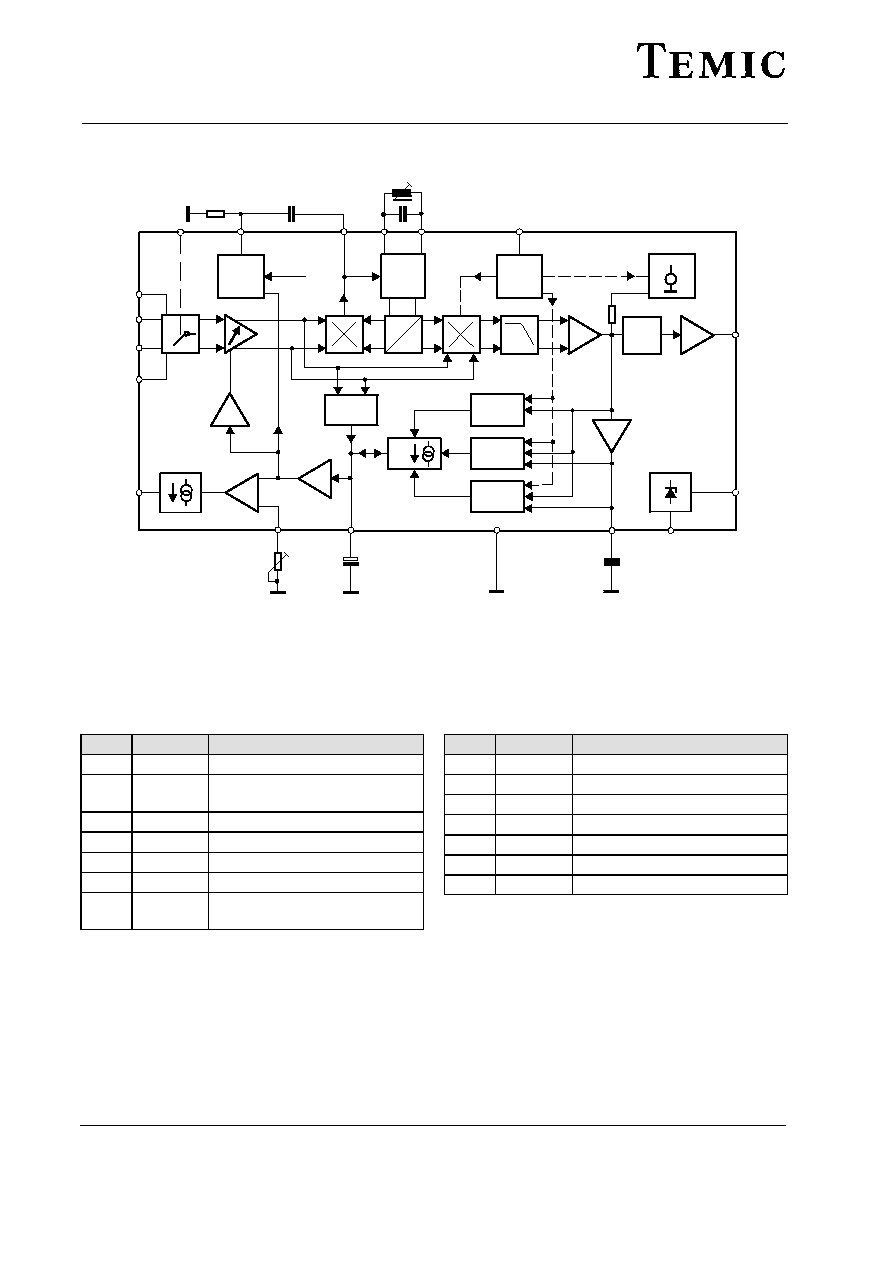
Block Diagram
90
∞
0
∞
Interference
rejection
Video
VCO
R
O
Video
output
7
Lock
detector
B/G
L
D2MAC
V
S
15
B/G
D2MAC
L
3
6
IF AGC
5
8
14
Average
(only L, D2MAC)
13
12
10
9
16
Loop filter
VCO Tank
11 Standard switch
Input
selector
switch
=
+
17
18
1
2
IF Input 1
4
Tuner AGC
93 7502
Tuner AGC
take over
Int. Ref
IF Input 2
Overload
detector
+/≠
Pin Description
Pin
Symbol
Function
1, 2
IF input 1
3
Tuner AGC adjustment (turn
over point)
4
Delayed tuner AGC current
5, 14
Ground
6
IF AGC time constant
7
Video output
8
Video averaging for standard L
and D2MAC
Pin
Symbol
Function
9, 10
VCO circuit
11
Standard switch
12
PLL loop filter
13
PLL time constant switch
15
Supply voltage
16
Input selector switch
17, 18
IF input 2

TELEFUNKEN Semiconductors
TDA4455
Preliminary Information
Rev. A1: 08.05.1995
3 (12)
Absolute Maximum Ratings
reference point Pin 4, unless otherwise specified
Parameters
Symbol
Value
Unit
¡¡¡¡¡¡¡¡¡¡¡¡¡¡¡¡¡
¡¡¡¡¡¡¡¡¡¡¡¡¡¡¡¡¡
Supply voltage
¡¡¡¡¡
¡¡¡¡¡
V
s
¡¡¡¡¡¡¡¡
¡¡¡¡¡¡¡¡
6.8 to 13.0
¡¡¡¡¡
¡¡¡¡¡
V
¡¡¡¡¡¡¡¡¡¡¡¡¡¡¡¡¡
¡¡¡¡¡¡¡¡¡¡¡¡¡¡¡¡¡
Supply current
¡¡¡¡¡
¡¡¡¡¡
I
S
¡¡¡¡¡¡¡¡
¡¡¡¡¡¡¡¡
60
¡¡¡¡¡
¡¡¡¡¡
mA
¡¡¡¡¡¡¡¡¡¡¡¡¡¡¡¡¡
¡¡¡¡¡¡¡¡¡¡¡¡¡¡¡¡¡
Output current
¡¡¡¡¡
¡¡¡¡¡
I
out
¡¡¡¡¡¡¡¡
¡¡¡¡¡¡¡¡
5.0
¡¡¡¡¡
¡¡¡¡¡
mA
¡¡¡¡¡¡¡¡¡¡¡¡¡¡¡¡¡
Maximum power dissipation
¡¡¡¡¡
P
¡¡¡¡¡¡¡¡
720
¡¡¡¡¡
mW
¡¡¡¡¡¡¡¡¡¡¡¡¡¡¡¡¡
¡¡¡¡¡¡¡¡¡¡¡¡¡¡¡¡¡
Junction temperature
¡¡¡¡¡
¡¡¡¡¡
T
j
¡¡¡¡¡¡¡¡
¡¡¡¡¡¡¡¡
+125
¡¡¡¡¡
¡¡¡¡¡
∞
C
¡¡¡¡¡¡¡¡¡¡¡¡¡¡¡¡¡
¡¡¡¡¡¡¡¡¡¡¡¡¡¡¡¡¡
Ambient temperature
¡¡¡¡¡
¡¡¡¡¡
T
amb
¡¡¡¡¡¡¡¡
¡¡¡¡¡¡¡¡
≠25 to +85
¡¡¡¡¡
¡¡¡¡¡
∞
C
¡¡¡¡¡¡¡¡¡¡¡¡¡¡¡¡¡
¡¡¡¡¡¡¡¡¡¡¡¡¡¡¡¡¡
Storage temperature
¡¡¡¡¡
¡¡¡¡¡
T
stg
¡¡¡¡¡¡¡¡
¡¡¡¡¡¡¡¡
≠25 to +125
¡¡¡¡¡
¡¡¡¡¡
∞
C
Thermal Resistance
Parameters
Symbol
Value
Unit
¡¡¡¡¡¡¡¡¡¡¡¡¡¡¡¡¡
Junction ambient (when soldered to PCB)
¡¡¡¡¡
R
thJA
¡¡¡¡¡¡¡¡
60
¡¡¡¡¡
K/W
External Voltage
Pin
Voltage range *)
¡¡¡¡¡¡¡¡¡
¡¡¡¡¡¡¡¡¡
1, 2
¡¡¡¡¡¡¡¡¡¡¡¡¡¡¡¡¡¡¡¡¡¡¡¡¡
¡¡¡¡¡¡¡¡¡¡¡¡¡¡¡¡¡¡¡¡¡¡¡¡¡
0
v Vpin v min (V
s
, 8 V)
¡¡¡¡¡¡¡¡¡
¡¡¡¡¡¡¡¡¡
3
¡¡¡¡¡¡¡¡¡¡¡¡¡¡¡¡¡¡¡¡¡¡¡¡¡
¡¡¡¡¡¡¡¡¡¡¡¡¡¡¡¡¡¡¡¡¡¡¡¡¡
0
v Vpin v V
s
¡¡¡¡¡¡¡¡¡
¡¡¡¡¡¡¡¡¡
4
¡¡¡¡¡¡¡¡¡¡¡¡¡¡¡¡¡¡¡¡¡¡¡¡¡
¡¡¡¡¡¡¡¡¡¡¡¡¡¡¡¡¡¡¡¡¡¡¡¡¡
0
v Vpin v min (V
s
, 10 V)
¡¡¡¡¡¡¡¡¡
¡¡¡¡¡¡¡¡¡
6
¡¡¡¡¡¡¡¡¡¡¡¡¡¡¡¡¡¡¡¡¡¡¡¡¡
¡¡¡¡¡¡¡¡¡¡¡¡¡¡¡¡¡¡¡¡¡¡¡¡¡
0
v Vpin v min (V
s
, 10 V)
¡¡¡¡¡¡¡¡¡
¡¡¡¡¡¡¡¡¡
7
¡¡¡¡¡¡¡¡¡¡¡¡¡¡¡¡¡¡¡¡¡¡¡¡¡
¡¡¡¡¡¡¡¡¡¡¡¡¡¡¡¡¡¡¡¡¡¡¡¡¡
0
v Vpin v 6 V
¡¡¡¡¡¡¡¡¡
¡¡¡¡¡¡¡¡¡
8
¡¡¡¡¡¡¡¡¡¡¡¡¡¡¡¡¡¡¡¡¡¡¡¡¡
¡¡¡¡¡¡¡¡¡¡¡¡¡¡¡¡¡¡¡¡¡¡¡¡¡
0
v Vpin v min (V
s
, 8 V)
¡¡¡¡¡¡¡¡¡
¡¡¡¡¡¡¡¡¡
9, 10
¡¡¡¡¡¡¡¡¡¡¡¡¡¡¡¡¡¡¡¡¡¡¡¡¡
¡¡¡¡¡¡¡¡¡¡¡¡¡¡¡¡¡¡¡¡¡¡¡¡¡
0
v Vpin v V
s
¡¡¡¡¡¡¡¡¡
¡
¡¡¡¡¡¡¡
¡
11
¡¡¡¡¡¡¡¡¡¡¡¡¡¡¡¡¡¡¡¡¡¡¡¡¡
¡¡¡¡¡¡¡¡¡¡¡¡¡¡¡¡¡¡¡¡¡¡¡¡
¡
0
v Vpin v V
s
¡¡¡¡¡¡¡¡¡
¡¡¡¡¡¡¡¡¡
12
¡¡¡¡¡¡¡¡¡¡¡¡¡¡¡¡¡¡¡¡¡¡¡¡¡
¡¡¡¡¡¡¡¡¡¡¡¡¡¡¡¡¡¡¡¡¡¡¡¡¡
0
v Vpin v min (V
s
, 7.5 V)
¡¡¡¡¡¡¡¡¡
¡¡¡¡¡¡¡¡¡
13
¡¡¡¡¡¡¡¡¡¡¡¡¡¡¡¡¡¡¡¡¡¡¡¡¡
¡¡¡¡¡¡¡¡¡¡¡¡¡¡¡¡¡¡¡¡¡¡¡¡¡
0
v Vpin v V
s
¡¡¡¡¡¡¡¡¡
¡¡¡¡¡¡¡¡¡
15
¡¡¡¡¡¡¡¡¡¡¡¡¡¡¡¡¡¡¡¡¡¡¡¡¡
¡¡¡¡¡¡¡¡¡¡¡¡¡¡¡¡¡¡¡¡¡¡¡¡¡
6.8 V
v Vpin v V
s
¡¡¡¡¡¡¡¡¡
¡¡¡¡¡¡¡¡¡
16
¡¡¡¡¡¡¡¡¡¡¡¡¡¡¡¡¡¡¡¡¡¡¡¡¡
¡¡¡¡¡¡¡¡¡¡¡¡¡¡¡¡¡¡¡¡¡¡¡¡¡
0
v Vpin v V
s
¡¡¡¡¡¡¡¡¡
¡¡¡¡¡¡¡¡¡
17, 18
¡¡¡¡¡¡¡¡¡¡¡¡¡¡¡¡¡¡¡¡¡¡¡¡¡
¡¡¡¡¡¡¡¡¡¡¡¡¡¡¡¡¡¡¡¡¡¡¡¡¡
0
v Vpin v min (V
s
, 8 V)
*)
min(V
s
, xV): the lesser of the two values is the lower limit

TELEFUNKEN Semiconductors
TDA4455
Preliminary Information
Rev. A1: 08.05.1995
4 (12)
Electrical Characteristics
Vs = 8 V, T
amb
= 25
∞
C, reference point Pin 5, unless otherwise specified
Parameters
Test Conditions / Pins
Symbol
Min.
Typ.
Max.
Unit
¡¡¡¡¡¡¡¡¡¡¡¡¡¡¡¡¡¡¡¡¡¡¡¡¡¡¡¡¡¡¡¡
¡¡¡¡¡¡¡¡¡¡¡¡¡¡¡¡¡¡¡¡¡¡¡¡¡¡¡¡¡¡¡¡
DC-supply
Pin 15
¡¡¡¡¡¡¡¡¡
¡¡¡¡¡¡¡¡¡
Supply voltage
¡¡¡¡¡¡¡¡¡
¡¡¡¡¡¡¡¡¡
¡¡¡¡
¡¡¡¡
V
s
¡¡¡¡
¡¡¡¡
6.8
¡¡¡¡
¡¡¡¡
8.0
¡¡¡¡
¡¡¡¡
13.0
¡¡¡¡
¡¡¡¡
V
¡¡¡¡¡¡¡¡¡
¡¡¡¡¡¡¡¡¡
Supply current
¡¡¡¡¡¡¡¡¡
¡¡¡¡¡¡¡¡¡
¡¡¡¡
¡¡¡¡
I
s
¡¡¡¡
¡¡¡¡
¡¡¡¡
¡¡¡¡
50
¡¡¡¡
¡¡¡¡
60
¡¡¡¡
¡¡¡¡
mA
¡¡¡¡¡¡¡¡¡¡¡¡¡¡¡¡¡¡¡¡¡¡¡¡¡¡¡¡¡¡¡¡
¡¡¡¡¡¡¡¡¡¡¡¡¡¡¡¡¡¡¡¡¡¡¡¡¡¡¡¡¡¡¡¡
IF-amplifier
Pins 1≠2 or Pins 17≠18
¡¡¡¡¡¡¡¡¡
¡¡¡¡¡¡¡¡¡
Input sensitivity
¡¡¡¡¡¡¡¡¡
¡¡¡¡¡¡¡¡¡
sync peak value, B/G
¡¡¡¡
¡¡¡¡
V
in
¡¡¡¡
¡¡¡¡
¡¡¡¡
¡¡¡¡
80
¡¡¡¡
¡¡¡¡
120
¡¡¡¡
¡¡¡¡
µ
V
eff
¡¡¡¡¡¡¡¡¡
¡¡¡¡¡¡¡¡¡
Input impedance
¡¡¡¡¡¡¡¡¡
¡¡¡¡¡¡¡¡¡
¡¡¡¡
¡¡¡¡
R
in
¡¡¡¡
¡¡¡¡
¡¡¡¡
¡¡¡¡
1.2
¡¡¡¡
¡¡¡¡
¡¡¡¡
¡¡¡¡
k
W
¡¡¡¡¡¡¡¡¡
¡¡¡¡¡¡¡¡¡
Input capacitance
¡¡¡¡¡¡¡¡¡
¡¡¡¡¡¡¡¡¡
¡¡¡¡
¡¡¡¡
C
in
¡¡¡¡
¡¡¡¡
¡¡¡¡
¡¡¡¡
2
¡¡¡¡
¡¡¡¡
¡¡¡¡
¡¡¡¡
pF
¡¡¡¡¡¡¡¡¡¡¡¡¡¡¡¡¡¡¡¡¡¡¡¡¡¡¡¡¡¡¡¡
¡¡¡¡¡¡¡¡¡¡¡¡¡¡¡¡¡¡¡¡¡¡¡¡¡¡¡¡¡¡¡¡
IF-AGC
Pins 6 and 8
¡¡¡¡¡¡¡¡¡
¡¡¡¡¡¡¡¡¡
IF gain control range
¡¡¡¡¡¡¡¡¡
¡¡¡¡¡¡¡¡¡
¡¡¡¡
¡¡¡¡
G
v
¡¡¡¡
¡¡¡¡
60
¡¡¡¡
¡¡¡¡
66
¡¡¡¡
¡¡¡¡
¡¡¡¡
¡¡¡¡
dB
¡¡¡¡¡¡¡¡¡
¡¡¡¡¡¡¡¡¡
Response time, standard L
¡¡¡¡¡¡¡¡¡
¡¡¡¡¡¡¡¡¡
Note 1
¡¡¡¡
¡¡¡¡
t
AGC
¡¡¡¡
¡¡¡¡
¡¡¡¡
¡¡¡¡
¡¡¡¡
¡¡¡¡
10
¡¡¡¡
¡¡¡¡
µ
sec
¡¡¡¡¡¡¡¡¡
¡¡¡¡¡¡¡¡¡
AGC capacitor
¡¡¡¡¡¡¡¡¡
¡¡¡¡¡¡¡¡¡
¡¡¡¡
¡¡¡¡
C
6
¡¡¡¡
¡¡¡¡
¡¡¡¡
¡¡¡¡
4,7
¡¡¡¡
¡¡¡¡
¡¡¡¡
¡¡¡¡
µ
F
¡¡¡¡¡¡¡¡¡
¡¡¡¡¡¡¡¡¡
Average capacitor
¡¡¡¡¡¡¡¡¡
¡¡¡¡¡¡¡¡¡
¡¡¡¡
¡¡¡¡
C
8
¡¡¡¡
¡¡¡¡
¡¡¡¡
¡¡¡¡
68
¡¡¡¡
¡¡¡¡
¡¡¡¡
¡¡¡¡
nF
¡¡¡¡¡¡¡¡¡¡¡¡¡¡¡¡¡¡¡¡¡¡¡¡¡¡¡¡¡¡¡¡
¡¡¡¡¡¡¡¡¡¡¡¡¡¡¡¡¡¡¡¡¡¡¡¡¡¡¡¡¡¡¡¡
Tuner-AGC
Pins 3 and 4
¡¡¡¡¡¡¡¡¡
¡¡¡¡¡¡¡¡¡
Available tuner-AGC
current
¡¡¡¡¡¡¡¡¡
¡¡¡¡¡¡¡¡¡
¡¡¡¡
¡¡¡¡
I
4
¡¡¡¡
¡¡¡¡
¡¡¡¡
¡¡¡¡
4
¡¡¡¡
¡¡¡¡
¡¡¡¡
¡¡¡¡
mA
¡¡¡¡¡¡¡¡¡
¡¡¡¡¡¡¡¡¡
Automatic turn over point
¡¡¡¡¡¡¡¡¡
¡¡¡¡¡¡¡¡¡
¡¡¡¡
¡¡¡¡
G
v,tun
¡¡¡¡
¡¡¡¡
¡¡¡¡
¡¡¡¡
65
¡¡¡¡
¡¡¡¡
¡¡¡¡
¡¡¡¡
dB
¡¡¡¡¡¡¡¡¡¡¡¡¡¡¡¡¡¡¡¡¡¡¡¡¡¡¡¡¡¡¡¡
¡¡¡¡¡¡¡¡¡¡¡¡¡¡¡¡¡¡¡¡¡¡¡¡¡¡¡¡¡¡¡¡
PLL
Pins 9≠10, 12, 13
see note 2
¡¡¡¡¡¡¡¡¡
¡¡¡¡¡¡¡¡¡
PLL capture range
¡¡¡¡¡¡¡¡¡
¡¡¡¡¡¡¡¡¡
¡¡¡¡
¡¡¡¡
Df
cap
¡¡¡¡
¡¡¡¡
¡¡¡¡
¡¡¡¡
±
1.5
¡¡¡¡
¡¡¡¡
¡¡¡¡
¡¡¡¡
MHz
¡¡¡¡¡¡¡¡¡
¡¡¡¡¡¡¡¡¡
VCO-tuning range
¡¡¡¡¡¡¡¡¡
¡¡¡¡¡¡¡¡¡
¡¡¡¡
¡¡¡¡
Df
vco
¡¡¡¡
¡¡¡¡
¡¡¡¡
¡¡¡¡
3.0
¡¡¡¡
¡¡¡¡
¡¡¡¡
¡¡¡¡
MHz
¡¡¡¡¡¡¡¡¡
¡¡¡¡¡¡¡¡¡
VCO-tuning sensitivity
¡¡¡¡¡¡¡¡¡
¡¡¡¡¡¡¡¡¡
¡¡¡¡
¡¡¡¡
Df / Du
¡¡¡¡
¡¡¡¡
3.0
¡¡¡¡
¡¡¡¡
4.5
¡¡¡¡
¡¡¡¡
¡¡¡¡
¡¡¡¡
kHz/mV
¡¡¡¡¡¡¡¡¡¡¡¡¡¡¡¡¡¡¡¡¡¡¡¡¡¡¡¡¡¡¡¡
¡¡¡¡¡¡¡¡¡¡¡¡¡¡¡¡¡¡¡¡¡¡¡¡¡¡¡¡¡¡¡¡
Video demodulator output
Pin 7
see note 3
¡¡¡¡¡¡¡¡¡
¡
¡¡¡¡¡¡¡
¡
¡¡¡¡¡¡¡¡¡
Composite video output
signal standard B/G
¡¡¡¡¡¡¡¡¡
¡
¡¡¡¡¡¡¡
¡
¡¡¡¡¡¡¡¡¡
Note 4
¡¡¡¡
¡
¡¡
¡
¡¡¡¡
V
out
¡¡¡¡
¡
¡¡
¡
¡¡¡¡
1.8
¡¡¡¡
¡
¡¡
¡
¡¡¡¡
2.0
¡¡¡¡
¡
¡¡
¡
¡¡¡¡
2.2
¡¡¡¡
¡
¡¡
¡
¡¡¡¡
V
pp
¡¡¡¡¡¡¡¡¡
¡
¡¡¡¡¡¡¡
¡
¡¡¡¡¡¡¡¡¡
Video output signal
standard L
¡¡¡¡¡¡¡¡¡
¡
¡¡¡¡¡¡¡
¡
¡¡¡¡¡¡¡¡¡
Note 5
¡¡¡¡
¡
¡¡
¡
¡¡¡¡
V
out
¡¡¡¡
¡
¡¡
¡
¡¡¡¡
1.2
¡¡¡¡
¡
¡¡
¡
¡¡¡¡
1.4
¡¡¡¡
¡
¡¡
¡
¡¡¡¡
1.6
¡¡¡¡
¡
¡¡
¡
¡¡¡¡
V
pp
¡¡¡¡¡¡¡¡¡
¡¡¡¡¡¡¡¡¡
Difference of the video
signals
¡¡¡¡¡¡¡¡¡
¡¡¡¡¡¡¡¡¡
Standard B/G and L
¡¡¡¡
¡¡¡¡
DV
out
¡¡¡¡
¡¡¡¡
¡¡¡¡
¡¡¡¡
¡¡¡¡
¡¡¡¡
10
¡¡¡¡
¡¡¡¡
%
¡¡¡¡¡¡¡¡¡
¡
¡¡¡¡¡¡¡
¡
¡¡¡¡¡¡¡¡¡
Ultra white level,
standard B/G
¡¡¡¡¡¡¡¡¡
¡
¡¡¡¡¡¡¡
¡
¡¡¡¡¡¡¡¡¡
Zero carrier level
¡¡¡¡
¡
¡¡
¡
¡¡¡¡
V
7
¡¡¡¡
¡
¡¡
¡
¡¡¡¡
¡¡¡¡
¡
¡¡
¡
¡¡¡¡
4.2
¡¡¡¡
¡
¡¡
¡
¡¡¡¡
¡¡¡¡
¡
¡¡
¡
¡¡¡¡
V
¡¡¡¡¡¡¡¡¡
¡¡¡¡¡¡¡¡¡
Ultra black level, Stand. L
¡¡¡¡¡¡¡¡¡
¡¡¡¡¡¡¡¡¡
Zero carrier level
¡¡¡¡
¡¡¡¡
V
7
¡¡¡¡
¡¡¡¡
¡¡¡¡
¡¡¡¡
1.9
¡¡¡¡
¡¡¡¡
¡¡¡¡
¡¡¡¡
V
¡¡¡¡¡¡¡¡¡
¡
¡¡¡¡¡¡¡
¡
¡¡¡¡¡¡¡¡¡
Supply voltage influence
on the ultra black level
(B /G)
¡¡¡¡¡¡¡¡¡
¡
¡¡¡¡¡¡¡
¡
¡¡¡¡¡¡¡¡¡
¡¡¡¡
¡
¡¡
¡
¡¡¡¡
DV/
V
¡¡¡¡
¡
¡¡
¡
¡¡¡¡
¡¡¡¡
¡
¡¡
¡
¡¡¡¡
0.5
¡¡¡¡
¡
¡¡
¡
¡¡¡¡
¡¡¡¡
¡
¡¡
¡
¡¡¡¡
%/V
¡¡¡¡¡¡¡¡¡
¡
¡¡¡¡¡¡¡
¡
¡¡¡¡¡¡¡¡¡
Supply voltage influence
on the ultra black level (L)
¡¡¡¡¡¡¡¡¡
¡
¡¡¡¡¡¡¡
¡
¡¡¡¡¡¡¡¡¡
¡¡¡¡
¡
¡¡
¡
¡¡¡¡
DV/
V
¡¡¡¡
¡
¡¡
¡
¡¡¡¡
¡¡¡¡
¡
¡¡
¡
¡¡¡¡
0.5
¡¡¡¡
¡
¡¡
¡
¡¡¡¡
¡¡¡¡
¡
¡¡
¡
¡¡¡¡
%/V
¡¡¡¡¡¡¡¡¡
¡¡¡¡¡¡¡¡¡
Video bandwidth (≠3 dB)
¡¡¡¡¡¡¡¡¡
¡¡¡¡¡¡¡¡¡
¡¡¡¡
¡¡¡¡
B
¡¡¡¡
¡¡¡¡
12
¡¡¡¡
¡¡¡¡
¡¡¡¡
¡¡¡¡
¡¡¡¡
¡¡¡¡
MHz
¡¡¡¡¡¡¡¡¡
¡¡¡¡¡¡¡¡¡
Video frequency response
over the AGC range
¡¡¡¡¡¡¡¡¡
¡¡¡¡¡¡¡¡¡
¡¡¡¡
¡¡¡¡
DB
¡¡¡¡
¡¡¡¡
¡¡¡¡
¡¡¡¡
¡¡¡¡
¡¡¡¡
2.0
¡¡¡¡
¡¡¡¡
dB
¡¡¡¡¡¡¡¡¡
¡¡¡¡¡¡¡¡¡
Differential gain error
¡¡¡¡¡¡¡¡¡
¡¡¡¡¡¡¡¡¡
¡¡¡¡
¡¡¡¡
DG
¡¡¡¡
¡¡¡¡
¡¡¡¡
¡¡¡¡
3
¡¡¡¡
¡¡¡¡
¡¡¡¡
¡¡¡¡
%
¡¡¡¡¡¡¡¡¡
¡¡¡¡¡¡¡¡¡
Differential phase error
¡¡¡¡¡¡¡¡¡
¡¡¡¡¡¡¡¡¡
¡¡¡¡
¡¡¡¡
DF
¡¡¡¡
¡¡¡¡
¡¡¡¡
¡¡¡¡
3
¡¡¡¡
¡¡¡¡
¡¡¡¡
¡¡¡¡
deg
Video demodulator output
Pin 7
¡¡¡¡¡¡¡¡¡
¡
¡¡¡¡¡¡¡
¡
¡
¡¡¡¡¡¡¡
¡
¡
¡¡¡¡¡¡¡
¡
¡¡¡¡¡¡¡¡¡
Sound chroma beat
(1.07 MHz intermodu-
lation) related to demodu-
lated auxiliary colour
carrier.
¡¡¡¡¡¡¡¡¡
¡
¡¡¡¡¡¡¡
¡
¡
¡¡¡¡¡¡¡
¡
¡
¡¡¡¡¡¡¡
¡
¡¡¡¡¡¡¡¡¡
Picture carrier = 0 dB
Colour carrier = ≠6 dB
Sound carrier = ≠24 dB
¡¡¡¡
¡
¡¡
¡
¡
¡¡
¡
¡
¡¡
¡
¡¡¡¡
a
IM
¡¡¡¡
¡
¡¡
¡
¡
¡¡
¡
¡
¡¡
¡
¡¡¡¡
52
¡¡¡¡
¡
¡¡
¡
¡
¡¡
¡
¡
¡¡
¡
¡¡¡¡
¡¡¡¡
¡
¡¡
¡
¡
¡¡
¡
¡
¡¡
¡
¡¡¡¡
¡¡¡¡
¡
¡¡
¡
¡
¡¡
¡
¡
¡¡
¡
¡¡¡¡
dB
TELEFUNKEN Semiconductors
TDA4455
Preliminary Information
Rev. A1: 08.05.1995
5 (12)
Unit
Max.
Typ.
Min.
Symbol
Test Conditions / Pins
Parameters
¡¡¡¡¡¡¡¡¡
¡
¡¡¡¡¡¡¡
¡
¡¡¡¡¡¡¡¡¡
IF residual voltage
f = 38.9 MHz
f = 77.8 MHz
¡¡¡¡¡¡¡¡¡
¡
¡¡¡¡¡¡¡
¡
¡¡¡¡¡¡¡¡¡
¡¡¡¡
¡
¡¡
¡
¡¡¡¡
V
res1
V
res2
¡¡¡¡
¡
¡¡
¡
¡¡¡¡
¡¡¡¡
¡
¡¡
¡
¡¡¡¡
2
5
¡¡¡¡
¡
¡¡
¡
¡¡¡¡
¡¡¡¡
¡
¡¡
¡
¡¡¡¡
mV
mV
¡¡¡¡¡¡¡¡¡
¡
¡¡¡¡¡¡¡
¡
¡¡¡¡¡¡¡¡¡
Upsetting factor of sync
pulse in the AGC range
¡¡¡¡¡¡¡¡¡
¡
¡¡¡¡¡¡¡
¡
¡¡¡¡¡¡¡¡¡
¡¡¡¡
¡
¡¡
¡
¡¡¡¡
DVsync
Vsync
¡¡¡¡
¡
¡¡
¡
¡¡¡¡
¡¡¡¡
¡
¡¡
¡
¡¡¡¡
3
¡¡¡¡
¡
¡¡
¡
¡¡¡¡
¡¡¡¡
¡
¡¡
¡
¡¡¡¡
%
¡¡¡¡¡¡¡¡¡
¡
¡¡¡¡¡¡¡
¡
Tilt of half picture
between black and white
¡¡¡¡¡¡¡¡¡
¡
¡¡¡¡¡¡¡
¡
Standard L
¡¡¡¡
¡
¡¡
¡
¡¡¡¡
¡
¡¡
¡
¡¡¡¡
¡
¡¡
¡
5
¡¡¡¡
¡
¡¡
¡
10
¡¡¡¡
¡
¡¡
¡
%
¡¡¡¡¡¡¡¡¡
¡
¡¡¡¡¡¡¡
¡
¡¡¡¡¡¡¡¡¡
Ultra black limiting
threshold
¡¡¡¡¡¡¡¡¡
¡
¡¡¡¡¡¡¡
¡
¡¡¡¡¡¡¡¡¡
Below sync level
¡¡¡¡
¡
¡¡
¡
¡¡¡¡
DV
lim1
¡¡¡¡
¡
¡¡
¡
¡¡¡¡
¡¡¡¡
¡
¡¡
¡
¡¡¡¡
250
¡¡¡¡
¡
¡¡
¡
¡¡¡¡
¡¡¡¡
¡
¡¡
¡
¡¡¡¡
mV
¡¡¡¡¡¡¡¡¡
¡
¡¡¡¡¡¡¡
¡
¡¡¡¡¡¡¡¡¡
Ultra white limiting
threshold
¡¡¡¡¡¡¡¡¡
¡
¡¡¡¡¡¡¡
¡
¡¡¡¡¡¡¡¡¡
Above ultra white level
¡¡¡¡
¡
¡¡
¡
¡¡¡¡
DV
lim2
¡¡¡¡
¡
¡¡
¡
¡¡¡¡
¡¡¡¡
¡
¡¡
¡
¡¡¡¡
500
¡¡¡¡
¡
¡¡
¡
¡¡¡¡
¡¡¡¡
¡
¡¡
¡
¡¡¡¡
mV
¡¡¡¡¡¡¡¡¡¡¡¡¡¡¡¡¡¡¡¡¡¡¡¡¡¡¡¡¡¡¡¡
¡¡¡¡¡¡¡¡¡¡¡¡¡¡¡¡¡¡¡¡¡¡¡¡¡¡¡¡¡¡¡¡
Standard switch
Pin 11
¡¡¡¡¡¡¡¡¡
Control voltage B/G
¡¡¡¡¡¡¡¡¡
Note 6
¡¡¡¡
V
sw1
¡¡¡¡
2.5
¡¡¡¡
¡¡¡¡
4.0
¡¡¡¡
V
¡¡¡¡¡¡¡¡¡
¡¡¡¡¡¡¡¡¡
Control voltage L
¡¡¡¡¡¡¡¡¡
¡¡¡¡¡¡¡¡¡
¡¡¡¡
¡¡¡¡
V
sw2
¡¡¡¡
¡¡¡¡
0
¡¡¡¡
¡¡¡¡
¡¡¡¡
¡¡¡¡
1.5
¡¡¡¡
¡¡¡¡
V
¡¡¡¡¡¡¡¡¡
¡¡¡¡¡¡¡¡¡
Control voltage D2MAC
¡¡¡¡¡¡¡¡¡
¡¡¡¡¡¡¡¡¡
¡¡¡¡
¡¡¡¡
V
sw3
¡¡¡¡
¡¡¡¡
5.0
¡¡¡¡
¡¡¡¡
¡¡¡¡
¡¡¡¡
V
s
¡¡¡¡
¡¡¡¡
V
Input selector switch
Pin 16
Control voltage ≠ input 1
active
Note 7
5.0
V
S
V
Control voltage ≠ input 2
active
0
2.5
V
Notes
1.
A peak white value for at least 10
µ
s must be trans-
mitted for each complete frame
2.
Loop filter: R1 = 500
W ≠ 1 k, C1 = 0.47 mF
Capacitor VCO circuit: C
VCO
= 27 ≠ 47 pF
3.
Pin 7 unloaded
4.
Residual carrier: 10% carrier amplitude
5.
Blanking level: 30% carrier amplitude
6.
Without control voltage at Pin 11 ≠ standard B/G is
automatically selected
7.
Without control voltage at Pin 16 ≠ input 1 is auto-
matically active
Alignment of the VCO
1.
Apply 4.5 V to Pin 6, to disable the broadband
amplifier.
2.
Measure the dc-voltage at Pin 12 (phase detector).
3.
Apply a 38.9 MHz unmodulated carrier signal to the
IF input (Pins 1≠2 or Pins 17≠18); adjust the input
level so that the AGC voltage at Pin 6 is between
2.0 V and 2.5 V.
4.
Adjust the VCO circuit until at Pin 12 is the same DC-
voltage as measured in step 2.