 | –≠–ª–µ–∫—Ç—Ä–æ–Ω–Ω—ã–π –∫–æ–º–ø–æ–Ω–µ–Ω—Ç: TFDT4000 | –°–∫–∞—á–∞—Ç—å:  PDF PDF  ZIP ZIP |

Edition January 7, 1996
1
TFDT4000
Integrated Transceiver
Description
The
TFDT4000
is an infrared transceiver for data communication systems. The
transceiver is compatible to the IRDA standard and allows data rates up to 115 kbit/sAn
internal AGC (Automatic Gain Control) ensures proper operation under EMI conditions.
The internal IRED driver can be connected by the external current control resistor to an
independent unregulated power supply. This will add more freedom in circuit design and
efficient serial drive capability for external IREDs for high power applications.
Features:
Compatible to IRDA standard
SMD top view and through hole side view
Wide supply voltage range (2.7V...5.5V)
Low Profile (height = 5.6 mm max.)
Microcomputer compatible
Fewest external components
Low power consumption
AGC for EMI immunity
Open collector IRED driver
Package:
Pins, see pg. 7:
1: IRED Anode
2: IRED Cathode
3: Txd (Input)
4: Rxd (Output)
5: NC
6: V
CC
(Supply Voltage)
7: SC (Sensitivity Control)
8: Ground
2 stand off pins internally connected to ground.
Block Diagram
6
Open Collector
Driver
Driver
Comparator
Amplifier
AGC
logic
8 GND
3 Txd
1
2
Rxd 4
Vcc
7 SC

Edition January 7, 1996
2
TFDT4000
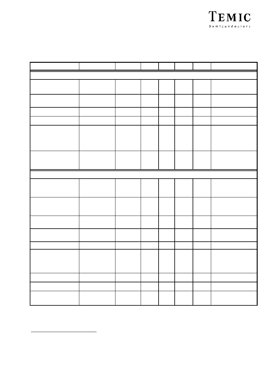
Absolute maximum ratings
Reference Point Pin 8, unless otherwise noted.
Parameter
Test Conditions
Symbol
MIN
TYP
MAX
Unit
Remark
Supply Voltage Range
V
cc
- 0.5
6
V
Voltage Range of IRED
Drive Output
pin 1,
Txd "LOW"
- 0.5
6
V
Input Currents
all pins
except 1, 8, see
IRED current
10
mA
Output Sinking Current
25
mA
Power Dissipation
Ptot
200
mW
s. derating curve, pg. 8
Junction Temperature
TJ
125
∞C
Ambient Temperature
Range (Operating)
Tamb
0
70
∞C
Storage temperature
range
Tstg
- 25
85
∞C
Soldering temperature
t= 20 s @215∞C
215
230
∞C
s. TEMIC IrDA Design
Guide
Average IRED current
IIRED(DC)
100
mA
Rep. pulsed IRED
current
IIRED(RP)
500
mA
<90µs, ton<20%
Peak IRED current
IIRED(PK)
1
A
<2µs, ton<10%
IRED Anode Voltage
VIREDA
- 0.5
V
cc
+0.5
V
Transmitter Data Input
Voltage
VTxd
- 0.5
V
cc
+0.5
V
Receiver Data Output
Voltage
VRxd
- 0.5
V
cc
+0.5
V

Edition January 7, 1996
3
TFDT4000
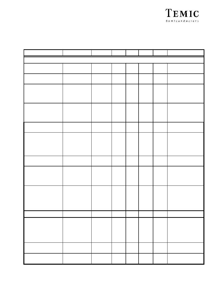
Optoelectronic characteristics
Tamb = 25∞C, V
cc
=5V unless otherwise noted.
Parameter
Test condition
Symbol
MIN
TYP
MAX
Unit
Remark
Transceiver
Supported data rates
Base band
2.4
115.2
kBit/s
IrDA SIR mode
Supply voltage range
V
cc
2.7
5
5.5
V
reduced function
down to 2.5V
Supply current, pin 6
V
cc
=5V
IS
1.3
2.5
mA
Supply current, pin 6
V
cc
=3V
IS
1.0
1.5
mA
Leakage current of
IR emitter , pin 1
V
cc
, pin 6: Off,
Txd: "LOW"
V
cc2
= 6V
T=-25∞C to 85∞C
IS
0.005
0.5
µA
s. appl. hint, page 6
Transceiver power on
settling time
50
µs
Time from switching
on V
cc
to established
specified operation
Receiver
Min. detection
threshold irradiance,
SC="LOW"
=
±
15∞
Eemin
0.020
0.035
Wm-2 SIR mode
)
Min. detection
threshold irradiance,
SC="HIGH"
=
±
15∞
Eemin
0.006
0.010
0.015
Wm-2 SIR mode **)
Max. detection
threshold irradiance
=
±
90∞, V
cc
=5V
Eemax
3300
5000
Wm-2 SIR mode **)
Max. detection
threshold irradiance
=
±
90∞, V
cc
=3V
Eemax
8000
15000
Wm-2 SIR mode **)
Logic Low Receiver
Input Irradiance,
SC="HIGH" or
SC="LOW"
Eemaxlow
0.004
Wm-2
Output voltage Rxd
active
VOL
0.5
0.8
V
C=15pF, R=2.2k
Output voltage Rxd
non active
VOH
V
cc
-0.5
V
C=15pF, R=2.2k
Output current
VOL<0.8V
4
mA
)
BER=10
-8
(IrDA specification)

Edition January 7, 1996
4
TFDT4000
Optoelectronic characteristics
Tamb = 25∞C, V
cc
=5V unless otherwise noted.
Parameter
Test condition
Symbol
MIN
TYP
MAX
Unit
Remark
Receiver, cont.
Rise time @load=
C=15pF, R=2.2k
t
r
20
200
ns
Fall time @load=
C=15pF, R=2.2k
t
f
20
200
ns
Rxd signal electrical
output pulse width
2.4 kBit/s, input
pulse length
1.41µs to 3/16 of
bit length
t
p
1.41
20
µs
Rxd signal electrical
output pulse width
115.2 kBit/s,
input pulse
length 1.41µs to
3/16 of bit length
t
p
1.41
8
µs
Rxd signal electrical
output pulse width
500 kHz, duty
cycle 50%
t
p
0.8
1
1.2
µs
V
cc
= 5 V only
Output delay time
(Rxd)
Output level =
0.5*V
cc
@
Ee=0.040 W/m2
t
dl
1
2
µs
Delay of leading edge
of output signal
related to leading
edge of optical input
signal
Jitter, leading edge of
output signal
Over a period of
10bit, 115.2 kBd
t
j
2
µs
Output delay time
(Rxd)
Output level =
0.5*V
cc
t
dt
6.5
µs
Delay of trailing edge
of output signal
related to trailing edge
of optical input signal
Latency
Recovery from
last transmitted
pulse to
1.1*threshold
sensitivity
t
L
100
800
µs
Transmitter
Driver current
IRED
Current limiting
resistor in series
to IRED:
RS= 8.2
@ 5 V
cc2
=5V
I
d
0.3
0.5
A
I
d
can be adjusted by
variation of R
S
, see
appl. hint page 6
Logic Low Transmitter
Input Voltage
VIL(Txd)
0
0.8
V
Logic High Transmitter
Input Voltage
VIH(Txd)
2.4
V
cc
V

Edition January 7, 1996
5
TFDT4000
Optoelectronic characteristics
Tamb = 25∞C, V
cc
=5V unless otherwise noted.
Parameter
Test condition
Symbol
MIN
TYP
MAX
Unit
Remark
Transmitter, cont.
Output Radiant
Intensity,
=
±
15∞
Current limiting
resistor in series
to IRED:
RS = 8.2
,
V
cc2
=5V
45
150
200
mW/sr in agreement with
prospective future eye
safety limits of
IEC825
Angle of half intensity
±
24
∞
Peak wavelength of
emission
p
850
900
nm
Halfwidth of Emission
Spectrum
60
nm
Optical Rise/Falltime
115.2 kHz
square wave
signal (duty
cycle: 1:1)
200
600
ns
Output Radiant
Intensity
logic low level
0.04
µW/sr
Overshoot, optical
25
%
Rising edge
peak to peak jitter
Over a period of
10 bits,
independent of
information
content
tj
0.2
µs


