Document Outline
- Description
- Features
- Block Diagram
- Pin Configuration
- Pin Description
- EPROM
- Electrical Characteristics
- Ordering Information

TSC87C52
1
MATRA MHS
Rev. C ≠ 10 Sept 1997
Preliminary
CMOS 0 to 33 MHz Programmable 8≠bit Microcontroller
Description
TEMIC's TSC87C52 is high performance CMOS
EPROM version of the 80C52 CMOS single chip 8 bit
microcontroller.
The fully static design of the TSC87C52 allows to
reduce system power consumption by bringing the clock
frequency down to any value, even DC, without loss of
data.
The TSC87C52 retains all the features of the 80C52 with
some enhancement: 8 K bytes of internal code memory
(EPROM); 256 bytes of internal data memory (RAM);
32 I/O lines; three 16 bit timers one with count≠down
and clock≠out capability; a 6-source, 2-level interrupt
structure; a full duplex serial port with framing error
detection; a power off flag; and an on-chip oscillator.
The TSC87C52 has 2 software-selectable modes of
reduced activity for further reduction in power
consumption. In the idle mode the CPU is frozen while
the RAM, the timers, the serial port and the interrupt
system continue to function. In the power down mode
the RAM is saved and all other functions are inoperative.
The TSC87C52 is manufactured using non volatile
SCMOS process which allows it to run up to:
D 33 MHz with VCC = 5 V
±
10%.
D 16 MHz with 2.7 V < VCC < 5.5 V.
Features
D 8 Kbytes of EPROM
G
Improved Quick Pulse programming algorithm
G
Secret ROM by encryption
D 256 bytes of RAM
D 64 Kbytes program memory space
D 64 Kbytes data memory space
D 32 programmable I/O lines
D Three 16 bit timer/counters including enhanced
timer 2
D Programmable serial port with framing error
detection
D Power control modes
D Two≠level interrupt priority
D Fully static design
D 0.8
µ
SCMOS non volatile process
D ONCE Mode
D Enhanced Hooks system for emulation purpose
D Available temperature ranges:
G commercial
G industrial
D Available packages:
G PDIP40 (OTP)
G PLCC44 (OTP)
G PQFP44 (OTP)
G CQPJ44 (UV erasable)
G CERDIP40 (UV erasable)

TSC87C52
2
Rev. C ≠ 10 Sept 1997
Preliminary
MATRA MHS
Block Diagram
EPROM
Figure 1 TSC87C52 Block diagram
TSC87C52
3
MATRA MHS
Rev. C ≠ 10 Sept 1997
Preliminary
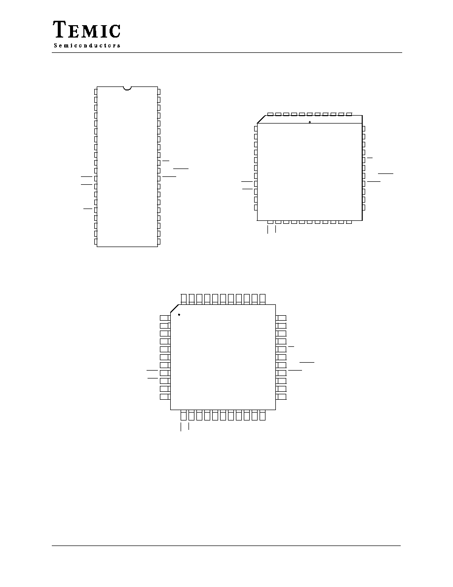
Pin Configuration
P1.0/T2
P1.1/T2EX
P1.2
P1.3
P1.4
P1.5
P1.6
P1.7
RST
P3.0/RxD
P3.1/TxD
P3.2/INT0
P3.3/INT1
P3.4/T0
P3.5/T1
P3.6/WR
P3.7/RD
XTAL2
XTAL1
VSS
39
PLCC/CQPJ
38
37
36
35
34
33
32
31
30
29
7
8
9
10
11
12
14
15
16
17
13
18 19
23
22
21
20
26
25
24
27 28
5 4 3 2 1
6
44 43 42 41 40
P1.4
P1.0/T2
P1.1/T2EX
P1.3
P1.2
VSS1
VCC
P0.0/AD0
P0.2/AD2
P0.3/AD3
P0.1/AD1
P0.4/AD4
P0.6/AD6
P0.5/AD5
P0.7/AD7
ALE/PROG
PSEN
EA/VPP
Reserved
P2.7/A15
P2.5/A13
P2.6/A14
P3.6/WR
P3.7/RD
XT
AL2
XT
AL1
VSS
Reserved
P2.0/A8
P2.1/A9
P2.2/A10
P2.3/A1
1
P2.4/A12
33
Flat Pack
32
31
30
29
28
27
26
25
24
23
1
2
3
4
5
6
8
9
10
11
7
12 13
17
16
15
14
20
19
18
21 22
43 42 41 40 39
44
38 37 36 35 34
P1.4
P1.0/T2
P1.1/T2EX
P1.3
P1.2
VSS1
VCC
P0.0/AD0
P0.2/AD2
P0.3/AD3
P0.1/AD1
P0.4/AD4
P0.6/AD6
P0.5/AD5
P0.7/AD7
ALE/PROG
PSEN
EA/VPP
Reserved
P2.7/A15
P2.5/A13
P2.6/A14
P1.5
P1.6
P1.7
RST
P3.0/RxD
Reserved
P3.1/TxD
P3.2/INT0
P3.3/INT1
P3.4/T0
P3.5/T1
P3.6/WR
P3.7/RD
XT
AL2
XT
AL1
VSS
Reserved
P2.0/A8
P2.1/A9
P2.2/A10
P2.3/A1
1
P2.4/A12
P1.5
P1.6
P1.7
RST
P3.0/RxD
Reserved
P3.1/TxD
P3.2/INT0
P3.3/INT1
P3.4/T0
P3.5/T1
VCC
P0.0
P0.1
P0.2
P0.3
P0.4
P0.5
P0.6
P0.7
EA/VPP
ALE/PROG
PSEN
P2.7
P2.6
P2.5
P2.4
P2.3
P2.2
P2.1
P2.0
1
2
3
4
5
6
7
8
9
10
11
12
13
14
15
16
17
18
19
20
40
39
38
37
36
35
34
33
32
31
30
29
28
27
26
25
24
23
22
21
DIP
Figure 2 TSC87C52 pin configuration
Do not connect Reserved pins.

TSC87C52
4
Rev. C ≠ 10 Sept 1997
Preliminary
MATRA MHS
Pin Description
VSS
Circuit ground potential.
VSS1
Secondary ground (not on DIP). Provided to reduce ground bounce and improve power supply by≠passing.
Note: This pin is not a substitute for the VSS pin. Connection is not necessary for proper operation.
VCC
Supply voltage during normal, Idle, and Power Down operation.
Port 0
Port 0 is an 8 bit open drain bi-directional I/O port. Port 0 pins that have 1's written to them float, and in that state can
be used as high-impedance inputs.
Port 0 is also the multiplexed low-order address and data bus during accesses to external Program and Data Memory.
In this application it uses strong internal pullups when emitting 1's.
Port 0 can sink eight LS TTL inputs.
Port 0 is used as data bus during EPROM programming and program verification.
Port 1
Port 1 is an 8 bit bi-directional I/O port with internal pullups. Port 1 pins that have 1's written to them are pulled high
by the internal pullups, and in that state can be used as inputs. As inputs, Port 1 pins that are externally being pulled
low will source current (IIL, in the DC parameters section) because of the internal pullups.
Port 1 can sink/ source three LS TTL inputs. It can drive CMOS inputs without external pullups.
Port1 also serves the functions of the following special features of the TSC87C52 as listed below:
Port Pin
Alternate Function
P1.0
P1.1
T2 (External Count input to Timer/Counter 2), Clock≠Out
T2EX (Timer/Counter 2 Capture/Reload Trigger and direction Control)
Port 1 receives the low≠order address byte during EPROM programming and program verification.
Port 2
Port 2 is an 8 bit bi-directional I/O port with internal pullups. Port 2 pins that have 1's written to them are pulled high
by the internal pullups, and in that state can be used as inputs. As inputs, Port 2 pins that are externally being pulled
low will source current (IIL, in the DC parameters section) because of the internal pullups.
Port 2 emits the high-order address byte during fetches from external Program Memory and during accesses to external
Data Memory that use 16 bit addresses (MOVX @DPTR). In this application, it uses strong internal pullups when
emitting 1's. During accesses to external Data Memory that use 8 bit addresses (MOVX @Ri), Port 2 emits the contents
of the P2 Special Function Register.
Port 2 can sink/source three LS TTL inputs. It can drive CMOS inputs without external pullups.
Some Port 2 pins receive the high≠order address bits and control signals during EPROM programming and program
verification.
Port 3
Port 3 is an 8 bit bi-directional I/O port with internal pullups. Port 3 pins that have 1's written to them are pulled high
by the internal pullups, and in that state can be used as inputs. As inputs, Port 3 pins that are externally being pulled
low will source current (IIL, in the DC parameters section) because of the pullups.

TSC87C52
5
MATRA MHS
Rev. C ≠ 10 Sept 1997
Preliminary
Port 3 also serves the functions of various special features of the TEMIC's C51 Family, as listed below:
Port Pin
Alternate Function
P3.0
P3.1
P3.2
P3.3
P3.4
P3.5
P3.6
P3.7
RxD (serial input port)
TxD (serial output port)
INT0 (external interrupt 0)
INT1 (external interrupt 1)
T0 (Timer 0 external input)
T1 (Timer 1 external input)
WR (external Data Memory write strobe)
RD (external Data Memory read strobe)
Port 3 can sink/source three LS TTL inputs. It can drive CMOS inputs without external pullups.
Some Port 3 pins receive control signals during EPROM programming and program verification.
RST
A high level on this pin for two machine cycles while the oscillator is running resets the device. An internal pull-down
resistor permits Power-On reset using only a capacitor connected to V
CC
. The port pins will be driven to their reset
condition when a minimum VIH1 voltage is applied whether the oscillator is started or not (asynchronous reset).
ALE/PROG
Address Latch Enable output for latching the low byte of the address during accesses to external memory. ALE is
activated as though for this purpose at a constant rate of 1/6 the oscillator frequency except during an external data
memory access at which time one ALE pulse is skipped.
ALE can sink/source 8 LS TTL inputs. It can drive CMOS inputs without external pullup.
If desired, to reduce EMI, ALE operation can be disabled by setting bit 0 of SFR location 8Eh (MSCON). With this
bit set, the pin is weakly pulled high. However, ALE remains active during MOVX, MOVC instructions and external
fetches. Setting the ALE disable bit has no effect if the microcontroller is in external execution mode (EA=0).
Throughout the remainder of this datasheet, ALE will refer to the signal coming out of the ALE/PROG pin, and the
pin will be referred to as the ALE/PROG pin.
PSEN
Program Store Enable output is the read strobe to external Program Memory. PSEN is activated twice each machine
cycle during fetches from external Program Memory. (However, when executing out of external Program Memory, two
activations of PSEN are skipped during each access to external Data Memory). PSEN is not activated during fetches
from internal Program Memory. PSEN can sink/source 8 LS TTL inputs. It can drive CMOS inputs without an external
pullup.
EA/VPP
External Access enable. EA must be strapped to VSS in order to enable the device to fetch code from external Program
Memory locations 0000h to FFFFh. Note however, that if any of the Security bits are programmed, EA will be internally
latched on reset.
EA should be strapped to VCC for internal program execution.
This pin also receives the programming supply voltage (VPP) during EPROM programming.
XTAL1
Input to the inverting amplifier that forms the oscillator. Receives the external oscillator signal when an external
oscillator is used.
XTAL2
Output from the inverting amplifier that forms the oscillator. This pin should be floated when an external oscillator
is used.