U4459B
TELEFUNKEN Semiconductors
Rev. A1, 15-Jul-96
1 (7)
IF Amplifier for Cable DVB Processing
Description
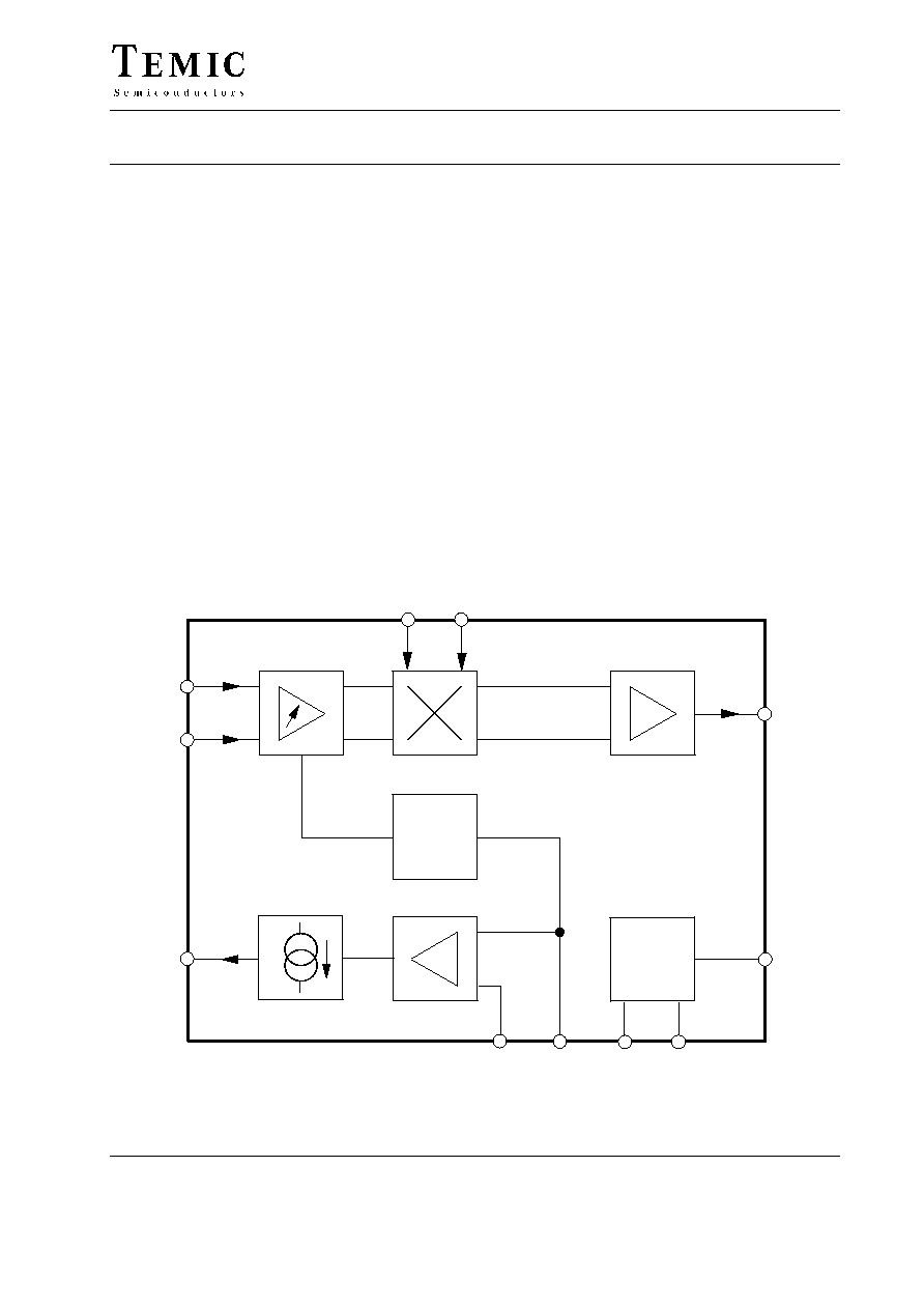
The U4459B is an integrated bipolar circuit suitable for
the IF processing in cable-DVB receiver (DVB = Digital
Video Broadcasting) and cable network application.
The circuit contains a wideband IF amplifier, mixer stage,
gain control for the IF amplifier and a tuner-AGC
(Automatic Gain Control) with adjustable take over point
for an additional external preamplifier (tuner).
Features
D Input frequency range 30 to 50 MHz (1st IF)
D Wideband IF amplifier with high linearity
D Gain control of the IF amplifier by external
dc voltage
D Mixer stage with local oscillator input
(symmetrical or unsymmetrical)
D High output level of mixed signal (2nd IF)
(up to 2.4 V, peak-to-peak value)
D Tuner-AGC with adjustable take over point for a
preamplifier
D Supply voltage range 6.8 to 13.5 V
Package: DIP16
1
16
3
IF1 in
8
9
5
13
2
IF1 in
Mixer
IF amp
IF gain
control
Bandgap
V
Tun
V
Gain
4,15
I
Tun
BG
GND
6
14
IF2 out
V
S
95 9636
LO in
LO in
Figure 1. Block diagram

U4459B
TELEFUNKEN Semiconductors
Rev. A1, 15-Jul-96
2 (7)
Pin Description
1
2
3
4
5
6
7
8
16
15
14
13
12
11
10
9
I
tun
GND
95 10696
V
gain
IF2
out
NC
IF1
in
V
tun
VS
BG
NC
NC
NC
LO
in
IF1
in
GND
LO
in
Figure 2.
Pin
Symbol
Function
���
���
1
����
����
IF1
in
�����������
�����������
IF1 input
���
���
2
����
����
V
tun
�����������
�����������
Take over point of tuner-AGC
���
���
3
����
����
I
tun
�����������
�����������
Tuner-AGC output current
���
���
4
����
����
GND
�����������
�����������
Ground
���
���
5
����
����
V
gain
�����������
�����������
IF gain control input
���
6
����
IF2
out
�����������
IF2 output
���
���
7
����
����
NC
�����������
�����������
Not connected
���
���
8
����
����
LO
in
�����������
�����������
Local oscillator input
���
���
9
����
����
LO
in
�����������
�����������
Local oscillator input
���
���
10
����
����
NC
�����������
�����������
Not connected
���
���
11
����
����
NC
�����������
�����������
Not connected
���
���
12
����
����
NC
�����������
�����������
Not connected
���
���
13
����
����
BG
�����������
�����������
Bandgap reference
(internal use only)
���
���
14
����
����
VS
�����������
�����������
Supply voltage
���
���
15
����
����
GND
�����������
�����������
Ground
���
���
16
����
����
IF1
in
�����������
�����������
IF1 input
Circuit Description
The U4459B consists of a controllable 3-stage wideband
amplifier, a mixer, IF-AGC and a tuner-AGC with
adjustable take over point. The IF1 input voltage is
applied at Pin 1 to 16 and it is fed via a 3-stage gain
controlled wideband amplifier to the mixer. The wide-
band amplifier with high linearity is gain controlled by
external dc voltage. The oscillator voltage (Pin 8�9) for
the mixer stage can be applied symmetrically as well as
unsymmetrically.
The mixed signal (2nd IF) is fed through a buffer
amplifier to the output Pin 6. The control voltage can also
be used for an additional external preamplifier in the
tuner. This tuner-AGC with adjustable take over point
protects the IF1 input against overload.
Absolute Maximum Ratings
Reference point Pin 4, unless otherwise specified
Parameters
Symbol
Value
Unit
�����������������
�����������������
Supply voltage
Pin 14
�����
�����
V
s
��������
��������
13.5
�����
�����
V
�����������������
�����������������
Supply current
Pin 14
�����
�����
I
s
��������
��������
55
�����
�����
mA
�����������������
�
���������������
�
�����������������
Power dissipation
V
s
= 13.5 V
Pin 14
�����
�
���
�
�����
P
��������
�
������
�
��������
750
�����
�
���
�
�����
mW
�����������������
�����������������
Junction temperature
�����
�����
T
j
��������
��������
+125
�����
�����
�
C
�����������������
�����������������
Storage temperature
�����
�����
T
stg
��������
��������
�25 to +125
�����
�����
�
C

U4459B
TELEFUNKEN Semiconductors
Rev. A1, 15-Jul-96
3 (7)
Operating Range
Parameters
Symbol
Value
Unit
�����������������
�����������������
Supply voltage range
Pin 14
�����
�����
V
s
��������
��������
6.8 to 13.5
�����
�����
V
�����������������
�����������������
Ambient temperature
�����
�����
T
amb
��������
��������
�10 to +80
�����
�����
�
C
Thermal Resistance
Parameters
Symbol
Value
Unit
�����������������
�����������������
Junction ambient when soldered to PCB
�����
�����
R
thJA
��������
��������
60
�����
�����
K/W
Electrical Characteristics
V
s
= +8 V, T
amb
= +25
�
C; reference point Pin 4, unless otherwise specified
Parameters
Test Conditions / Pins
Symbol
Min.
Typ.
Max.
Unit
��������������������������������
��������������������������������
DC supply
Pin 14
���������
���������
Supply voltage
���������
���������
����
����
V
S
����
����
6.8
����
����
8.0
����
����
13.5
����
����
V
���������
���������
Supply current
���������
���������
����
����
I
S
����
����
����
����
45
����
����
55
����
����
mA
��������������������������������
��������������������������������
IF1 input, 1st IF
Pin 1�16
���������
�
�������
�
���������
Input sensitivity
(RMS value)
���������
�
�������
�
���������
Output voltage 2 V
pp
����
�
��
�
����
V
IF1
����
�
��
�
����
����
�
��
�
����
80
����
�
��
�
����
120
����
�
��
�
����
�
V
RMS
���������
���������
IF1 input frequency range *)
���������
���������
����
����
f
in
����
����
30
����
����
����
����
50
����
����
MHz
���������
���������
Input impedance
���������
���������
����
����
R
in
����
����
����
����
1.2
����
����
����
����
k
W
���������
���������
Input capacitance
���������
���������
����
����
C
in
����
����
����
����
2
����
����
����
����
pF
��������������������������������
��������������������������������
IF gain control input
Pin 5
���������
���������
IF gain control range
���������
���������
Output voltage 2 V
pp
����
����
G
v
����
����
60
����
����
66
����
����
����
����
dB
��������������������������������
��������������������������������
Local oscillator input
Pin 8�9
���������
���������
Input voltage (RMS value)
���������
���������
����
����
v
LO
����
����
����
����
100
����
����
����
����
mV
RMS
���������
���������
Input frequency range *)
���������
���������
����
����
f
LO
����
����
30
����
����
����
����
50
����
����
MHz
��������������������������������
��������������������������������
IF2 output, 2nd IF
Pin 6
���������
���������
DC output voltage
���������
���������
V
5
= 3 V
����
����
V
DC
����
����
����
����
3.1
����
����
����
����
V
���������
���������
Upper limiting level
���������
���������
����
����
V
lim
����
����
����
����
4.5
����
����
����
����
V
���������
���������
Lower limiting level
���������
���������
����
����
V
lim
����
����
����
����
1.7
����
����
����
����
V
���������
���������
IF2 signal bandwidth
(� 3 dB) *)
���������
���������
Output voltage 2 V
pp
����
����
B
����
����
12
����
����
����
����
����
����
MHz
���������
�
�������
�
���������
Residual carrier,
fundamental wave
���������
�
�������
�
���������
����
�
��
�
����
v
res
����
�
��
�
����
����
�
��
�
����
����
�
��
�
����
20
����
�
��
�
����
mV
���������
�
�������
�
���������
Output current
�source
�sink
���������
�
�������
�
���������
����
�
��
�
����
I
out
����
�
��
�
����
1.5
����
�
��
�
����
����
�
��
�
����
5.0
2.5
����
�
��
�
����
mA
��������������������������������
��������������������������������
Tuner-AGC
���������
���������
Available AGC current
���������
���������
����
����
I
tun
����
����
2.0
����
����
4.0
����
����
6.0
����
����
mA
*)
Not measured during production

U4459B
TELEFUNKEN Semiconductors
Rev. A1, 15-Jul-96
4 (7)
16
15
14
13
1
2
3
4
U4459B
12
11
10
5
6
7
9
8
10 nF
10
mF
22
mH
4.7
mF
+V
S
200
W
10 nF
2:1
LO
input
Tuner AGC
IF2 out
IF gain
control
Tuner AGC
take over
10 k
W
10 nF
1:2
200
W
IF1
input
95 9637
10 nF
10 nF
*)
*) depends on application
1
mF to 10 mF
95 9637
Figure 3. Test circuit
16
15
14
13
1
2
3
4
U4459B
12
11
10
5
6
7
9
8
10 nF
10
mF
22
mH
+V
S
200
W
10 nF
2:1
LO
input
Tuner AGC
IF2 out
IF gain
control
Tuner AGC
take over
10 k
W
95 9638
SAW filter
IF1
in
10 nF
10 nF
*)
*) depends on application
1
mF to 10 mF
Figure 4. Basic application circuit

U4459B
TELEFUNKEN Semiconductors
Rev. A1, 15-Jul-96
5 (7)
Internal Pin Configuration
1.2 k
W
1.2 k
W
1
16
3 k
W
3 k
W
94 9227
Figure 5. IF1 input
8
5.6 k
W
94 9243
5.6 k
W
9
Figure 6. Local oscillator input
94 9242
6
Figure 7. IF2 output
94 9230
50
W
5
Figure 8. IF gain control input
2
94 9228
3 k
W
2 k
W
Figure 9. Tuner-AGC take over point
3
94 9229
Figure 10. Tuner-AGC output