 | –≠–ª–µ–∫—Ç—Ä–æ–Ω–Ω—ã–π –∫–æ–º–ø–æ–Ω–µ–Ω—Ç: U842B | –°–∫–∞—á–∞—Ç—å:  PDF PDF  ZIP ZIP |

U842B
TELEFUNKEN Semiconductors
Rev. A2, 03-Feb-97
1 (12)
Wiper Control for Intermittent and Wipe/ Wash Mode
Description
The U842B circuit is designed as an interval and
wipe/ wash timer for automotive wiper control. The
interval pause can be set in a range from 3 s to 11 s by an
external 1-k
W potentiometer. Wipe/wash mode has
priority over the interval mode. The U842B controls the
wiper motor with/without park switch signal.
The integrated relay driver is protected against short
circuits and is switched to conductive condition in the
case of a load-dump. With only a few external
components, protection against RF interference and
transients (ISO/TR 7637-1/3) can be achieved.
Features
D Interval input: low side
D Wipe/ wash input: low side
D Park input: high side (park position)
D Output driver protected against short circuit
D All time periods determined by RC oscillator
D Fixed relay activation time of 500 ms
D Adjustable interval pause from 3 s to 11 s
D Fixed pre-wash delay of 400 ms
D Dry wiping
≠ With park switch signal: 3 cycles
≠ Without park switch signal: 2.8 s
D Inputs INT, WASH and PARK digitally debounced
D All inputs with integrated RF protection
D Load-dump protection and interference protection ac-
cording to ISO 7637-1/3 (DIN 40839)
Application
Digital/ wipe-wash control for rear or front wiper
Ordring Information
Extended Type Number
Package
Remarks
U842B
DIP8
U842B≠FP
SO8
Pin Description
Pin
Symbol
Function
1
INT
Interval input
2
WASH
Wipe/ wash input
3
PARK
Park switch input
4
PAUS
Pause time adjust
5
OSC
Oscillator input
6
V
S
Supply voltage
7
GND
Ground
8
OUT
Relay output
1
2
3
4
8
7
6
5
INT
WASH
PARK
PAUS
OSC
Vs
GND
13300
OUT
U842B
Figure 1. Pinning

U842B
TELEFUNKEN Semiconductors
Rev. A2, 03-Feb-97
2 (12)
Block Diagram
+
≠
21 V
25 pF
+
≠
21 V
25 pF
+
≠
21 V
25 pF
Stabilization
POR
Load≠dump ≠
detection
V
S
21 V
Logic
28 V
+
≠
250 mV
0.5
Oscillator
+
≠
V
S
21 V
25 pF
21 V
Upper
switching
point
1/2 V
S
6
GND
7
8
OUT
5
OUT
OSC
4
INT
1
WASH
2
PARK
3
13287
PAUS
Figure 2. Block diagram
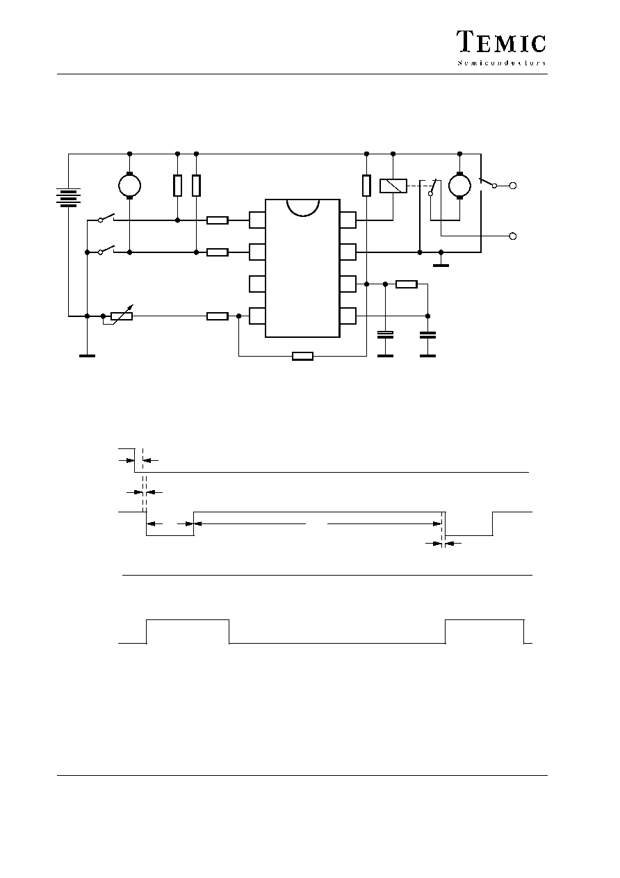
Basic Circuit
Power Supply
For reasons of interference protection and surge immu-
nity, a RC circuitry has to be provided to limit the current,
and to supply the integrated circuit in the case of supply
voltage drops.
Suggested values: R
1
= 180
W, C
1
= 47
mF,
(see figure 2)
The supply (Pin 6) is clamped with a 21-V Zener diode.
The operation voltage ranges between V
Batt
= 9 V to 16 V.
The capacitor, C
1,
can be dimensioned smaller (typically:
10
mF) if a diode is used in the supply against polarity re-
versal. In this case of negative interference pulses, there,
is only a small discharge current of the circuit.
Oscillator
All timing sequences in the circuit are derived from an RC
oscillator which is charged by an external resistor, R
9,
and
discharged by an integrated 2-k
W resistor. The basic
frequency, f
0,
is determined by the capacitor, C
2,
and an
integrated voltage divider. The basic frequency is
adjusted to 320 Hz ( 3.125 ms ) by C
2
= 100 nF and
R
9
= 220 k
W.
The tolerances and the temperature coefficients of the ex-
ternal components determine the precision of the
oscillator frequency. A 1% metallic-film resistor and a
5% capacitor are recommended..
The debouncing times of the inputs, the turn-on time of
the relay (t
5
), the pre-wash delay (t
1
), the dry wiping time
(t
2
) and the debouncing time (t
7
, short circuit detection)
depend on the oscillator frequency (f
0
) as follows:

U842B
TELEFUNKEN Semiconductors
Rev. A2, 03-Feb-97
3 (12)
C
1
13288
8
7
6
5
1
2
3
4
U842B
1.5 k
R
7
R
9
220 k
C
2
100 nF
180
R
1
47
µ
F
V
Batt
47 k
R
5
10 k
R
6
10 k
R
4
360
R
11
Switch
INT
Button
WASH
PARK
1 k
VR
1
Figure 3. Basic cicuitry
Variable Debouncing Times
Debouncing is basically done by counting oscillator
clocks starting with the occurance of any input signal.
Caused by the asynchronism of input signal and IC-clock,
the debouncing time may vary in a certain range.
Figure 4 shows the short circuit debouncing as an
example:
During the relay activation, a comparator monitors the
output current at each positive edge of the clock to load
a 3-stage shift register in the case of a detected short cir-
cuit condition i.e., I > 500 mA. With the third edge, the
output stage is disabled. Dependent on the short circuit
occurence the delay time may range from 2 to 3 clock
cycles.
The timing can be adjusted by variation of the external
frequency-determining components ( R/C ).
The potentiometer at Pin 4 determines the interval pause,
which can be varied by adjusting the upper charging
threshold of the oscillator. For all other time periods, an
internal voltage divider determines the upper charging
threshold of the oscillator (see figure 2).
Timing
Fixed:
Relay activation time
t
5
=
160
1/f
0
Dry wiping
t
2
= 896
1/f
0
or 3 cycles
Interval pause
t
6
= 872
1/f
0
Switch-on delay INT
t
4D
= 8
1/f
0
Variable:
Debouncing time INT
t
4
=
24 to 32
1/f
0
Debouncing time WASH
1. pre-wash delay
t
1
=
112 to 128
1/f
0
2. reverse debouncing
t
1.R
=
16 to 32
1/f
0
Debouncing time PARK
t
8
=
6 to 8
1/f
0
Debouncing time SC
t
7
=
2 to 3
1/f
0

U842B
TELEFUNKEN Semiconductors
Rev. A2, 03-Feb-97
4 (12)
Wipe/ Wash Operation
3
2
1
7
t
SC
CL
ON
OFF
OUT
IC>500mA
0
……………
……………
13301
Figure 4. The debouncing of the short circuit detection
Relay Output
The relay output is an open collector Darlington transistor
with an integrated 28-V Z-diode for limitation of the
inductive cut-out pulse of the relay coil. The maximum
static collector current must not exceed 300 mA and the
saturation voltage is typically 1.2 V for a current of
200 mA.
The collector current is permanently measured by an inte-
grated shunt, and in the case of a short circuit
(I
C
> 500 mA) to V
bat
, the relay output is stored disabled.
The short circuit buffer is reset by opening the INT and
WASH switches. As long as the short condition exists a
further activation of these switches will disable the output
stage again. Otherwise the normal wipe operation is per-
formed.
In order to avoid short-term disabling caused by current
pulses of transients, a 10 ms debounce period (t
7
) is pro-
vided (see figure 4).
During a load-dump pulse, the output transistor is
switched to conductive condition to prevent destruction.
The short circuit detection is suppressed during the load-
dump.
Interference Voltages and Load-dump
The IC supply is protected by R
1
, C
1
and an integrated
21-V Z-diode. The inputs are protected by a series
resistor, integrated 21-V Z-diode and RF capacitor.
The RC-configuration stabilizes the supply of the circuit
during negative interference voltages to avoid power-on
reset ( POR ).
The relay output is protected against short interference
peaks by an integrated 28-V Z-diode. During load-dump,
the relay output is switched to conductive condition if the
battery voltage exceeds approximately 30 V. The output
transistor is dimensioned so that it can absorb the current
produced by the load-dump pulse.
Power-on Reset
When the operating voltage is switched on, an internal
power-on reset pulse ( POR ) is generated which sets the
logic of the circuits to defined initial condition. The relay
output is disabled, the short circuit buffer is reset.
Functional Description
Interval Function
The circuit is brought to its interval mode with the input
switch INT operated for more than 625 ms
( t > t
4
+ t
4D
+t
5
).
This time includes:
≠ 100 ms debounce time t
4
≠ 25 ms INT switch-on delay t
4D
≠ 500 ms relay activation time t
5
If the INT input is toggled for 125 ms < t < 625 ms, the
relay activation time t
5
lapses anyway and the wiper
performs one turn. To enable correct interval functioning,
the INT input has to be activated afterwards as described.
The beginning of the interval pause depends on the
application with or without wiper motor park switch ( see
figures 5, 6, 7 and 8 ).

U842B
TELEFUNKEN Semiconductors
Rev. A2, 03-Feb-97
5 (12)
Interval Function with Park-Switch Feedback
During the relay activation time the wiper motor leaves
its park position and the park switch changes its potential
from V
Batt
to GND. After the relay is switched off the
wiper motor is supplied via the park switch until the park
position is reached again. The park switch changes its
potential from GND back to V
Batt
. With the park switch
connected to the park input (Pin 3) the interval pause t
6
starts after the 25 ms debounce time (t
7
) is over (see
figures 5 and 6).
13289
8
7
6
5
1
2
3
4
U842B
R
4
10 k
R
5
47 k
R
6
10 k
R
11
360
1.5 k
R
3
M
Wash
pump
1.5 k
R
2
INT
WASH
VR
1
1 k
SETINT
C
1
47
µ
F
180
R
1
R
7
1.5 k
R
9
220 k
C
2
100 nF
M
Wiper motor
Park
Run
Figure 5. Application circuit with park switch feedback
t
4D
V
0V
t
5
t
4
t
INT
8
OUT
PARK
MOTOR
ON
OFF
6
t
4D
t
Batt
V
0V
Batt
V
0V
Batt
13302
Figure 6. Intermittent circuit function with park position feedback
U842B
TELEFUNKEN Semiconductors
Rev. A2, 03-Feb-97
6 (12)
Interval Function without Park-Switch Feedback
If the park input of the circuit is not connected with the
park switch of the wiper motor (see figure 7), the interval
pause starts directly after the turn-on time of the relay is
over (see figure 8).
13290
8
7
6
5
1
2
3
4
U842B
R
4
10 k
R
5
47 k
R
11
1.5 k
R
3
M
Wash
pump
1.5 k
R
2
INT
WASH
VR
1
1 k
SETINT
C
1
47
µ
F
180
R
1
R
7
20 k
R
9
220 k
C
2
100 nF
M
Wiper motor
Park
Run
5.1 k
Figure 7. Application circuit without park position feedback
t
4D
6
t
OFF
ON
MOTOR
PARK
OUT
INT
t
4
t
5
0V
V
4D
t
Batt
0V
V
Batt
0V
V
Batt
13303
Figure 8. Intermittent circuit function without park position feedback

U842B
TELEFUNKEN Semiconductors
Rev. A2, 03-Feb-97
7 (12)
WASH
V
OFF
ON
MOTOR
OUT
PARK
<t
1
t
1R
wipe1
wipe2
wipe3
0V
t
1
t
7
Batt
V
0V
Batt
V
0V
Batt
13304
Figure 9. Wash operation with park switch signal
After operating the WASH switch, the relay is activated
after the debounce time, t
1
. As long as the switch is
pushed, water is sprayed on the windscreen by the wash
pump. When it is released, the dry wiping starts after 100
ms reverse debouncing (t
1R
).
Wipe/ Wash Mode with Park Position Feedback
If the park input of the circuit is connected to the park
switch, the dry wiping lasts three full wipe cycles (see
figure 9). During the third cycle, the wiper motor is sup-
plied via the park switch because the relay driver is
switched off after the second cycle.
Wipe/ Wash Mode without Park Position Feedback
If U842B is used without the wiper motor's park switch,
Pin 3 stays at high potential via its integrated pull-up
resistor. Therefore, the driver stage switches off after the
fixed dry wiping time t
2
.
t
1
WASH
V
OFF
ON
0V
MOTOR
OUT
PARK
<t
1
t
2
t
1R
Batt
V
0V
Batt
V
0V
Batt
13305
Figure 10. Wash operation without park signal report
U842B
TELEFUNKEN Semiconductors
Rev. A2, 03-Feb-97
8 (12)
Wipe/ Wash Mode Priority
The wipe/wash mode has priority over the interval mode
≠ therefore the interval function is interrupted as soon as
the WASH switch is operated longer than the debounce
time t
1
. With or without park switch feedback, after relay
activation time is over (no park switch feedback), or after
the third wipe (park switch feedback), the interval mode
is continued with an interval pause t
6
(see figures 11
and 12).
6
t
0V
5
PARK
OUT
ON
OFF
WASH
INT
V
t
MOTOR
t
4D
Batt
0V
V
Batt
0V
V
Batt
0V
V
Batt
13306
Figure 11. Wipe/ wash priority with park position feedback
4D
t
MOTOR
t
V
INT
WASH
OFF
ON
OUT
PARK
5
t
2
0V
t
6
Batt
V
0V
Batt
V
0V
Batt
V
0V
Batt
13307
Figure 12. Wash/ wipe priority without park position feedback
U842B
TELEFUNKEN Semiconductors
Rev. A2, 03-Feb-97
9 (12)
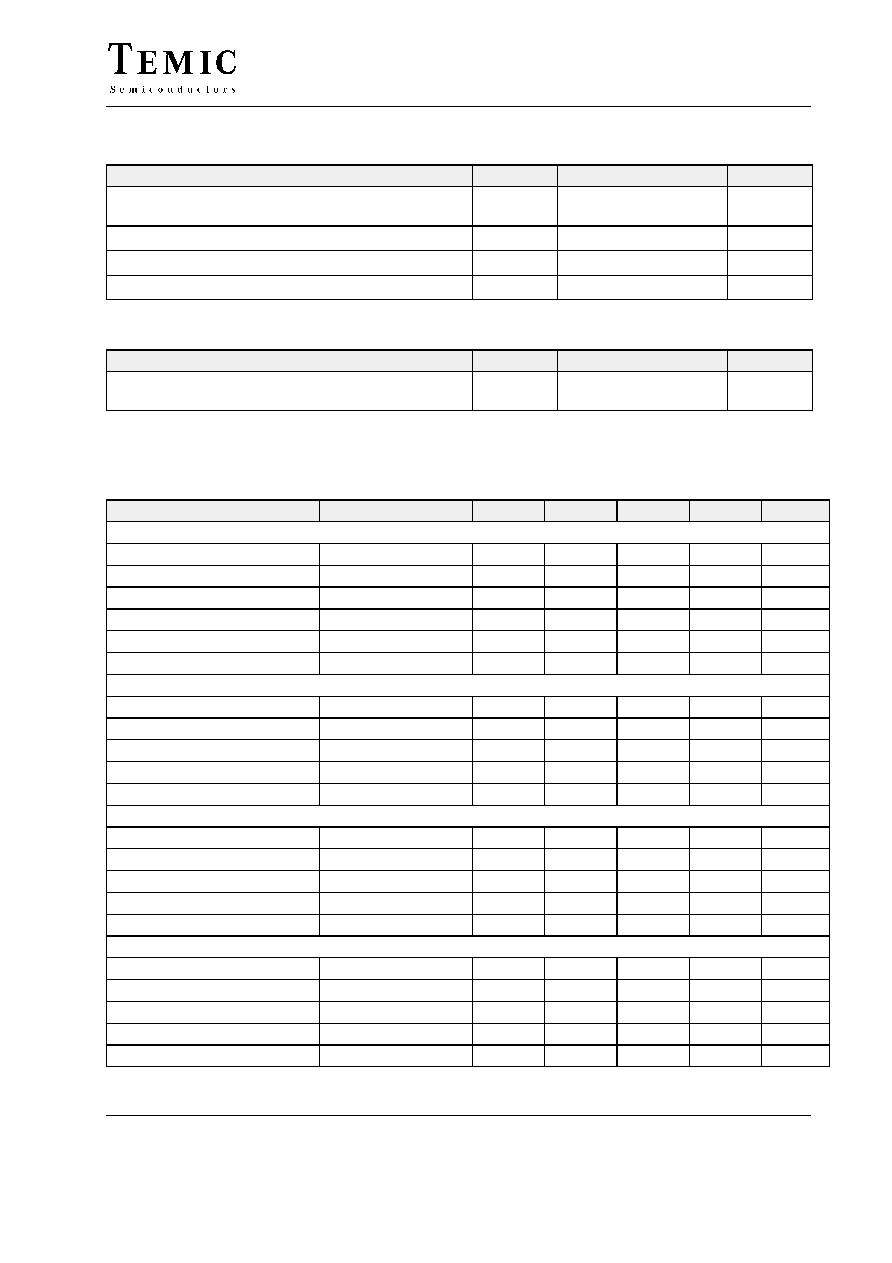
Absolute Maximum Ratings
Parameters
Symbol
Value
Unit
¡¡¡¡¡¡¡¡¡¡¡¡¡¡¡¡¡
¡¡¡¡¡¡¡¡¡¡¡¡¡¡¡¡¡
Supply voltage
t = 60 s
t = 600 s
¡¡¡¡¡
¡¡¡¡¡
V
Batt
V
Batt
¡¡¡¡¡¡¡¡
¡¡¡¡¡¡¡¡
24
18
¡¡¡¡¡
¡¡¡¡¡
V
V
¡¡¡¡¡¡¡¡¡¡¡¡¡¡¡¡¡
¡¡¡¡¡¡¡¡¡¡¡¡¡¡¡¡¡
Ambient temperature range
¡¡¡¡¡
¡¡¡¡¡
T
amb
¡¡¡¡¡¡¡¡
¡¡¡¡¡¡¡¡
≠30 to +100
¡¡¡¡¡
¡¡¡¡¡
∞
C
¡¡¡¡¡¡¡¡¡¡¡¡¡¡¡¡¡
¡
¡¡¡¡¡¡¡¡¡¡¡¡¡¡¡
¡
Storage temperature range
¡¡¡¡¡
¡
¡¡¡
¡
T
stg
¡¡¡¡¡¡¡¡
¡
¡¡¡¡¡¡
¡
≠40 to +100
¡¡¡¡¡
¡
¡¡¡
¡
∞
C
¡¡¡¡¡¡¡¡¡¡¡¡¡¡¡¡¡
¡
¡¡¡¡¡¡¡¡¡¡¡¡¡¡¡
¡
¡¡¡¡¡¡¡¡¡¡¡¡¡¡¡¡¡
Maximum junction temperature
¡¡¡¡¡
¡
¡¡¡
¡
¡¡¡¡¡
T
j
¡¡¡¡¡¡¡¡
¡
¡¡¡¡¡¡
¡
¡¡¡¡¡¡¡¡
150
¡¡¡¡¡
¡
¡¡¡
¡
¡¡¡¡¡
∞
C
Thermal Resistance
Parameters
Symbol
Maximum
Unit
¡¡¡¡¡¡¡¡¡¡¡¡¡¡¡¡¡
¡¡¡¡¡¡¡¡¡¡¡¡¡¡¡¡¡
Thermal resistance
DIP8
SO8
¡¡¡¡¡
¡¡¡¡¡
R
thja
R
thja
¡¡¡¡¡¡¡¡
¡¡¡¡¡¡¡¡
110
160
¡¡¡¡¡
¡¡¡¡¡
K/W
K/W
Electrical Characteristics
V
Batt
= 13.5 V, T
amb
= 25
∞
C, reference point ground (Pin 7), circuit with recommended external circuitry
(see figure 2)
Parameters
Test Conditions / Pin
Symbol
Min
Typ
Max
Unit
¡¡¡¡¡¡¡¡¡¡¡¡¡¡¡¡¡¡¡¡¡¡¡¡¡¡¡¡¡¡¡¡¡
¡¡¡¡¡¡¡¡¡¡¡¡¡¡¡¡¡¡¡¡¡¡¡¡¡¡¡¡¡¡¡¡¡
Supply
¡¡¡¡¡¡¡¡¡¡
¡¡¡¡¡¡¡¡¡¡
Supply-voltage range
¡¡¡¡¡¡¡¡
¡¡¡¡¡¡¡¡
¡¡¡¡
¡¡¡¡
V
S
¡¡¡¡
¡¡¡¡
9
¡¡¡¡
¡¡¡¡
¡¡¡¡¡
¡¡¡¡¡
16
¡¡¡
¡¡¡
V
¡¡¡¡¡¡¡¡¡¡
¡¡¡¡¡¡¡¡¡¡
Supply currrent
¡¡¡¡¡¡¡¡
¡¡¡¡¡¡¡¡
¡¡¡¡
¡¡¡¡
I
6
¡¡¡¡
¡¡¡¡
¡¡¡¡
¡¡¡¡
¡¡¡¡¡
¡¡¡¡¡
3
¡¡¡
¡¡¡
mA
¡¡¡¡¡¡¡¡¡¡
¡¡¡¡¡¡¡¡¡¡
Undervoltage threshold POR
¡¡¡¡¡¡¡¡
¡¡¡¡¡¡¡¡
¡¡¡¡
¡¡¡¡
V
6
¡¡¡¡
¡¡¡¡
¡¡¡¡
¡¡¡¡
3.5
¡¡¡¡¡
¡¡¡¡¡
¡¡¡
¡¡¡
V
¡¡¡¡¡¡¡¡¡¡
¡¡¡¡¡¡¡¡¡¡
Series resistance
¡¡¡¡¡¡¡¡
¡¡¡¡¡¡¡¡
¡¡¡¡
¡¡¡¡
R
1
¡¡¡¡
¡¡¡¡
¡¡¡¡
¡¡¡¡
180
¡¡¡¡¡
¡¡¡¡¡
¡¡¡
¡¡¡
W
¡¡¡¡¡¡¡¡¡¡
¡¡¡¡¡¡¡¡¡¡
Filter capacitance
¡¡¡¡¡¡¡¡
¡¡¡¡¡¡¡¡
¡¡¡¡
¡¡¡¡
C
1
¡¡¡¡
¡¡¡¡
¡¡¡¡
¡¡¡¡
47
¡¡¡¡¡
¡¡¡¡¡
¡¡¡
¡¡¡
mF
¡¡¡¡¡¡¡¡¡¡
¡¡¡¡¡¡¡¡¡¡
Internal Z-diode
¡¡¡¡¡¡¡¡
¡¡¡¡¡¡¡¡
¡¡¡¡
¡¡¡¡
V
6
¡¡¡¡
¡¡¡¡
¡¡¡¡
¡¡¡¡
21
¡¡¡¡¡
¡¡¡¡¡
¡¡¡
¡¡¡
V
INT input
Pin 1
¡¡¡¡¡¡¡¡¡¡
¡¡¡¡¡¡¡¡¡¡
Protective diode
¡¡¡¡¡¡¡¡
¡¡¡¡¡¡¡¡
¡¡¡¡
¡¡¡¡
V
1
¡¡¡¡
¡¡¡¡
¡¡¡¡
¡¡¡¡
21
¡¡¡¡¡
¡¡¡¡¡
¡¡¡
¡¡¡
V
¡¡¡¡¡¡¡¡¡¡
¡¡¡¡¡¡¡¡¡¡
Internal capacitance
¡¡¡¡¡¡¡¡
¡¡¡¡¡¡¡¡
¡¡¡¡
¡¡¡¡
C
1
¡¡¡¡
¡¡¡¡
¡¡¡¡
¡¡¡¡
25
¡¡¡¡¡
¡¡¡¡¡
¡¡¡
¡¡¡
pF
¡¡¡¡¡¡¡¡¡¡
¡¡¡¡¡¡¡¡¡¡
Threshold
¡¡¡¡¡¡¡¡
¡¡¡¡¡¡¡¡
¡¡¡¡
¡¡¡¡
V
1
¡¡¡¡
¡¡¡¡
¡¡¡¡
¡¡¡¡
0.5 V
6
¡¡¡¡¡
¡¡¡¡¡
¡¡¡
¡¡¡
W
¡¡¡¡¡¡¡¡¡¡
¡
¡¡¡¡¡¡¡¡
¡
Pull-up resistance
¡¡¡¡¡¡¡¡
¡
¡¡¡¡¡¡
¡
¡¡¡¡
¡
¡¡
¡
R
1
¡¡¡¡
¡
¡¡
¡
¡¡¡¡
¡
¡¡
¡
20
¡¡¡¡¡
¡
¡¡¡
¡
¡¡¡
¡¡¡
k
W
¡¡¡¡¡¡¡¡¡¡
¡¡¡¡¡¡¡¡¡¡
External series resistance
¡¡¡¡¡¡¡¡
¡¡¡¡¡¡¡¡
¡¡¡¡
¡¡¡¡
R
S
¡¡¡¡
¡¡¡¡
¡¡¡¡
¡¡¡¡
10
¡¡¡¡¡
¡¡¡¡¡
¡¡¡
¡¡¡
k
W
PARK input
Pin 3
¡¡¡¡¡¡¡¡¡¡
¡¡¡¡¡¡¡¡¡¡
Protective diode
¡¡¡¡¡¡¡¡
¡¡¡¡¡¡¡¡
¡¡¡¡
¡¡¡¡
V
3
¡¡¡¡
¡¡¡¡
¡¡¡¡
¡¡¡¡
21
¡¡¡¡¡
¡¡¡¡¡
¡¡¡
¡¡¡
V
¡¡¡¡¡¡¡¡¡¡
¡¡¡¡¡¡¡¡¡¡
Internal capacitance
¡¡¡¡¡¡¡¡
¡¡¡¡¡¡¡¡
¡¡¡¡
¡¡¡¡
C
3
¡¡¡¡
¡¡¡¡
¡¡¡¡
¡¡¡¡
25
¡¡¡¡¡
¡¡¡¡¡
¡¡¡
¡¡¡
pF
¡¡¡¡¡¡¡¡¡¡
¡¡¡¡¡¡¡¡¡¡
Threshold
¡¡¡¡¡¡¡¡
¡¡¡¡¡¡¡¡
¡¡¡¡
¡¡¡¡
V
3
¡¡¡¡
¡¡¡¡
¡¡¡¡
¡¡¡¡
0.5 V
6
¡¡¡¡¡
¡¡¡¡¡
¡¡¡
¡¡¡
W
¡¡¡¡¡¡¡¡¡¡
¡¡¡¡¡¡¡¡¡¡
Pull-up resistance
¡¡¡¡¡¡¡¡
¡¡¡¡¡¡¡¡
¡¡¡¡
¡¡¡¡
R
3
¡¡¡¡
¡¡¡¡
¡¡¡¡
¡¡¡¡
20
¡¡¡¡¡
¡¡¡¡¡
¡¡¡
¡¡¡
k
W
¡¡¡¡¡¡¡¡¡¡
¡¡¡¡¡¡¡¡¡¡
External series resistance
¡¡¡¡¡¡¡¡
¡¡¡¡¡¡¡¡
¡¡¡¡
¡¡¡¡
R
S
¡¡¡¡
¡¡¡¡
¡¡¡¡
¡¡¡¡
10
¡¡¡¡¡
¡¡¡¡¡
¡¡¡
¡¡¡
k
W
WASH input
Pin 2
¡¡¡¡¡¡¡¡¡¡
¡¡¡¡¡¡¡¡¡¡
Protective diode
¡¡¡¡¡¡¡¡
¡¡¡¡¡¡¡¡
¡¡¡¡
¡¡¡¡
V
2
¡¡¡¡
¡¡¡¡
¡¡¡¡
¡¡¡¡
21
¡¡¡¡¡
¡¡¡¡¡
¡¡¡
¡¡¡
V
¡¡¡¡¡¡¡¡¡¡
¡¡¡¡¡¡¡¡¡¡
Internal capacitance
¡¡¡¡¡¡¡¡
¡¡¡¡¡¡¡¡
¡¡¡¡
¡¡¡¡
C
2
¡¡¡¡
¡¡¡¡
¡¡¡¡
¡¡¡¡
25
¡¡¡¡¡
¡¡¡¡¡
¡¡¡
¡¡¡
pF
¡¡¡¡¡¡¡¡¡¡
¡¡¡¡¡¡¡¡¡¡
Threshold
¡¡¡¡¡¡¡¡
¡¡¡¡¡¡¡¡
¡¡¡¡
¡¡¡¡
V
2
¡¡¡¡
¡¡¡¡
¡¡¡¡
¡¡¡¡
0.5 V
6
¡¡¡¡¡
¡¡¡¡¡
¡¡¡
¡¡¡
W
¡¡¡¡¡¡¡¡¡¡
¡¡¡¡¡¡¡¡¡¡
Pull-up resistance
¡¡¡¡¡¡¡¡
¡¡¡¡¡¡¡¡
¡¡¡¡
¡¡¡¡
R
2
¡¡¡¡
¡¡¡¡
¡¡¡¡
¡¡¡¡
100
¡¡¡¡¡
¡¡¡¡¡
¡¡¡
¡¡¡
k
W
¡¡¡¡¡¡¡¡¡¡
¡¡¡¡¡¡¡¡¡¡
External series resistance
¡¡¡¡¡¡¡¡
¡¡¡¡¡¡¡¡
¡¡¡¡
¡¡¡¡
R
S
¡¡¡¡
¡¡¡¡
¡¡¡¡
¡¡¡¡
47
¡¡¡¡¡
¡¡¡¡¡
¡¡¡
¡¡¡
k
W

U842B
TELEFUNKEN Semiconductors
Rev. A2, 03-Feb-97
10 (12)
Parameters
Test Conditions / Pin
Symbol
Min
Typ
Max
Unit
PAUS input
Pin 4
¡¡¡¡¡¡¡¡¡¡
¡¡¡¡¡¡¡¡¡¡
Protective diode
¡¡¡¡¡¡¡¡
¡¡¡¡¡¡¡¡
¡¡¡¡
¡¡¡¡
V
4
¡¡¡¡
¡¡¡¡
¡¡¡¡
¡¡¡¡
21
¡¡¡¡
¡¡¡¡
¡¡¡¡
¡¡¡¡
V
¡¡¡¡¡¡¡¡¡¡
¡¡¡¡¡¡¡¡¡¡
Internal capacitance
¡¡¡¡¡¡¡¡
¡¡¡¡¡¡¡¡
¡¡¡¡
¡¡¡¡
C
4
¡¡¡¡
¡¡¡¡
¡¡¡¡
¡¡¡¡
25
¡¡¡¡
¡¡¡¡
¡¡¡¡
¡¡¡¡
pF
Relay output
Pin 8
¡¡¡¡¡¡¡¡¡¡
¡¡¡¡¡¡¡¡¡¡
Saturation voltage 100 mA
¡¡¡¡¡¡¡¡
¡¡¡¡¡¡¡¡
¡¡¡¡
¡¡¡¡
V
8
¡¡¡¡
¡¡¡¡
¡¡¡¡
¡¡¡¡
1.0
¡¡¡¡
¡¡¡¡
¡¡¡¡
¡¡¡¡
V
¡¡¡¡¡¡¡¡¡¡
¡¡¡¡¡¡¡¡¡¡
Saturation voltage 200 mA
¡¡¡¡¡¡¡¡
¡¡¡¡¡¡¡¡
¡¡¡¡
¡¡¡¡
V
8
¡¡¡¡
¡¡¡¡
¡¡¡¡
¡¡¡¡
1.2
¡¡¡¡
¡¡¡¡
¡¡¡¡
¡¡¡¡
V
¡¡¡¡¡¡¡¡¡¡
¡¡¡¡¡¡¡¡¡¡
Relay coil resistance
¡¡¡¡¡¡¡¡
¡¡¡¡¡¡¡¡
¡¡¡¡
¡¡¡¡
R
Rel
¡¡¡¡
¡¡¡¡
60
¡¡¡¡
¡¡¡¡
¡¡¡¡
¡¡¡¡
¡¡¡¡
¡¡¡¡
W
¡¡¡¡¡¡¡¡¡¡
¡¡¡¡¡¡¡¡¡¡
Output current
¡¡¡¡¡¡¡¡
¡¡¡¡¡¡¡¡
¡¡¡¡
¡¡¡¡
I
8
¡¡¡¡
¡¡¡¡
¡¡¡¡
¡¡¡¡
¡¡¡¡
¡¡¡¡
300
¡¡¡¡
¡¡¡¡
mA
¡¡¡¡¡¡¡¡¡¡
¡
¡¡¡¡¡¡¡¡
¡
¡¡¡¡¡¡¡¡¡¡
Normal operation
¡¡¡¡¡¡¡¡
¡
¡¡¡¡¡¡
¡
¡¡¡¡¡¡¡¡
¡¡¡¡
¡
¡¡
¡
¡¡¡¡
¡¡¡¡
¡
¡¡
¡
¡¡¡¡
¡¡¡¡
¡
¡¡
¡
¡¡¡¡
¡¡¡¡
¡
¡¡¡
¡¡¡¡
¡¡¡¡
¡
¡¡
¡
¡¡¡¡
¡¡¡¡¡¡¡¡¡¡
¡
¡¡¡¡¡¡¡¡
¡
Output pulse current
¡¡¡¡¡¡¡¡
¡
¡¡¡¡¡¡
¡
¡¡¡¡
¡
¡¡
¡
I
8
¡¡¡¡
¡
¡¡
¡
¡¡¡¡
¡
¡¡
¡
¡¡¡¡
¡
¡¡¡
1.5
¡¡¡¡
¡
¡¡
¡
A
¡¡¡¡¡¡¡¡¡¡
¡¡¡¡¡¡¡¡¡¡
Load-dump
¡¡¡¡¡¡¡¡
¡¡¡¡¡¡¡¡
¡¡¡¡
¡¡¡¡
¡¡¡¡
¡¡¡¡
¡¡¡¡
¡¡¡¡
¡¡¡¡
¡¡¡¡
¡¡¡¡
¡¡¡¡
¡¡¡¡¡¡¡¡¡¡
¡¡¡¡¡¡¡¡¡¡
Internal Z-diode
¡¡¡¡¡¡¡¡
¡¡¡¡¡¡¡¡
¡¡¡¡
¡¡¡¡
V
8
¡¡¡¡
¡¡¡¡
¡¡¡¡
¡¡¡¡
28
¡¡¡¡
¡¡¡¡
¡¡¡¡
¡¡¡¡
V
¡¡¡¡¡¡¡¡¡¡
¡¡¡¡¡¡¡¡¡¡
Short circuit threshold
¡¡¡¡¡¡¡¡
¡¡¡¡¡¡¡¡
¡¡¡¡
¡¡¡¡
I
8
¡¡¡¡
¡¡¡¡
500
¡¡¡¡
¡¡¡¡
¡¡¡¡
¡¡¡¡
¡¡¡¡
¡¡¡¡
mA
Oscillator input
Pin 5
¡¡¡¡¡¡¡¡¡¡
¡¡¡¡¡¡¡¡¡¡
Oscillator capacitor
¡¡¡¡¡¡¡¡
¡¡¡¡¡¡¡¡
Pin 5
¡¡¡¡
¡¡¡¡
C
2
¡¡¡¡
¡¡¡¡
¡¡¡¡
¡¡¡¡
100
¡¡¡¡
¡¡¡¡
¡¡¡¡
¡¡¡¡
nF
¡¡¡¡¡¡¡¡¡¡
¡¡¡¡¡¡¡¡¡¡
Oscillator resistor
¡¡¡¡¡¡¡¡
¡¡¡¡¡¡¡¡
Pins 5 and 6
¡¡¡¡
¡¡¡¡
R
8
¡¡¡¡
¡¡¡¡
¡¡¡¡
¡¡¡¡
220
¡¡¡¡
¡¡¡¡
¡¡¡¡
¡¡¡¡
k
W
¡¡¡¡¡¡¡¡¡¡
¡¡¡¡¡¡¡¡¡¡
Basic frequency
¡¡¡¡¡¡¡¡
¡¡¡¡¡¡¡¡
¡¡¡¡
¡¡¡¡
f
0
¡¡¡¡
¡¡¡¡
¡¡¡¡
¡¡¡¡
320
¡¡¡¡
¡¡¡¡
¡¡¡¡
¡¡¡¡
Hz
¡¡¡¡¡¡¡¡¡¡
¡¡¡¡¡¡¡¡¡¡
Lower switching point
¡¡¡¡¡¡¡¡
¡¡¡¡¡¡¡¡
¡¡¡¡
¡¡¡¡
V
5
¡¡¡¡
¡¡¡¡
¡¡¡¡
¡¡¡¡
0.07 V
6
¡¡¡¡
¡¡¡¡
¡¡¡¡
¡¡¡¡
¡¡¡¡¡¡¡¡¡¡
¡¡¡¡¡¡¡¡¡¡
Upper switching point
¡¡¡¡¡¡¡¡
¡¡¡¡¡¡¡¡
External 1 k
W pot.
¡¡¡¡
¡¡¡¡
V
5
¡¡¡¡
¡¡¡¡
0.2 V
6
¡¡¡¡
¡¡¡¡
¡¡¡¡
¡¡¡¡
0.5 V
6
¡¡¡¡
¡¡¡¡
¡¡¡¡¡¡¡¡¡¡
¡¡¡¡¡¡¡¡¡¡
Internal discharge resistance
¡¡¡¡¡¡¡¡
¡¡¡¡¡¡¡¡
¡¡¡¡
¡¡¡¡
R
5
¡¡¡¡
¡¡¡¡
¡¡¡¡
¡¡¡¡
2
¡¡¡¡
¡¡¡¡
¡¡¡¡
¡¡¡¡
k
W
¡¡¡¡¡¡¡¡¡¡
¡¡¡¡¡¡¡¡¡¡
Protective diode
¡¡¡¡¡¡¡¡
¡¡¡¡¡¡¡¡
V
F
= forward voltage
¡¡¡¡
¡¡¡¡
V
5
¡¡¡¡
¡¡¡¡
¡¡¡¡
¡¡¡¡
V
S
+ V
F
¡¡¡¡
¡¡¡¡
¡¡¡¡
¡¡¡¡
V
Times
External circuitry ≠ see oscillator input (figure 3)
¡¡¡¡¡¡¡¡¡¡
¡
¡¡¡¡¡¡¡¡
¡
¡
¡¡¡¡¡¡¡¡
¡
¡
¡¡¡¡¡¡¡¡
¡
¡
¡¡¡¡¡¡¡¡
¡
¡
¡¡¡¡¡¡¡¡
¡
¡¡¡¡¡¡¡¡¡¡
Debouncing times:
INT input
WASH input
Pre-wash delay
Reverse delay
Park
Short circuit
¡¡¡¡¡¡¡¡
¡
¡¡¡¡¡¡
¡
¡
¡¡¡¡¡¡
¡
¡
¡¡¡¡¡¡
¡
¡
¡¡¡¡¡¡
¡
¡
¡¡¡¡¡¡
¡
¡¡¡¡¡¡¡¡
¡¡¡¡
¡
¡¡
¡
¡
¡¡
¡
¡
¡¡
¡
¡
¡¡
¡
¡
¡¡
¡
¡¡¡¡
t
4
t
1
t
1,R
t
8
t
7
¡¡¡¡
¡
¡¡
¡
¡
¡¡
¡
¡
¡¡
¡
¡
¡¡
¡
¡
¡¡
¡
¡¡¡¡
50
260
50
14
5
¡¡¡¡
¡
¡¡
¡
¡
¡¡
¡
¡
¡¡
¡
¡
¡¡
¡
¡
¡¡
¡
¡¡¡¡
¡¡¡¡
¡
¡¡¡
¡
¡¡¡
¡
¡¡¡
¡
¡¡¡
¡
¡¡¡
¡¡¡¡
125
540
125
37
12
¡¡¡¡
¡
¡¡
¡
¡
¡¡
¡
¡
¡¡
¡
¡
¡¡
¡
¡
¡¡
¡
¡¡¡¡
ms
ms
ms
ms
ms
¡¡¡¡¡¡¡¡¡¡
¡¡¡¡¡¡¡¡¡¡
Switch-on delay (interval mode)
¡¡¡¡¡¡¡¡
¡¡¡¡¡¡¡¡
¡¡¡¡
¡¡¡¡
t
4D
¡¡¡¡
¡¡¡¡
18
¡¡¡¡
¡¡¡¡
¡¡¡¡
¡¡¡¡
31
¡¡¡¡
¡¡¡¡
ms
¡¡¡¡¡¡¡¡¡¡
¡¡¡¡¡¡¡¡¡¡
Relay activation time
¡¡¡¡¡¡¡¡
¡¡¡¡¡¡¡¡
¡¡¡¡
¡¡¡¡
t
5
¡¡¡¡
¡¡¡¡
400
¡¡¡¡
¡¡¡¡
¡¡¡¡
¡¡¡¡
625
¡¡¡¡
¡¡¡¡
ms
¡¡¡¡¡¡¡¡¡¡
¡¡¡¡¡¡¡¡¡¡
Interval pause
¡¡¡¡¡¡¡¡
¡¡¡¡¡¡¡¡
¡¡¡¡
¡¡¡¡
t
6
¡¡¡¡
¡¡¡¡
2.25
¡¡¡¡
¡¡¡¡
¡¡¡¡
¡¡¡¡
13.75
¡¡¡¡
¡¡¡¡
s
¡¡¡¡¡¡¡¡¡¡
¡¡¡¡¡¡¡¡¡¡
Dry wiping
¡¡¡¡¡¡¡¡
¡¡¡¡¡¡¡¡
¡¡¡¡
¡¡¡¡
¡¡¡¡
¡¡¡¡
¡¡¡¡
¡¡¡¡
¡¡¡¡
¡¡¡¡
¡¡¡¡
¡¡¡¡
¡¡¡¡¡¡¡¡¡¡
¡¡¡¡¡¡¡¡¡¡
Without park switch feedback
¡¡¡¡¡¡¡¡
¡¡¡¡¡¡¡¡
¡¡¡¡
¡¡¡¡
t
2
¡¡¡¡
¡¡¡¡
2.1
¡¡¡¡
¡¡¡¡
¡¡¡¡
¡¡¡¡
3.5
¡¡¡¡
¡¡¡¡
s
¡¡¡¡¡¡¡¡¡¡
¡¡¡¡¡¡¡¡¡¡
With park switch feedback
¡¡¡¡¡¡¡¡
¡¡¡¡¡¡¡¡
¡¡¡¡
¡¡¡¡
¡¡¡¡
¡¡¡¡
¡¡¡¡
¡¡¡¡
3
¡¡¡¡
¡¡¡¡
¡¡¡¡
¡¡¡¡
wipes

U842B
TELEFUNKEN Semiconductors
Rev. A2, 03-Feb-97
11 (12)
Package Information
13021
9.8
9.5
Package DIP8
Dimensions in mm
1.64
1.44
4.8 max
0.5 min
3.3
0.58
0.48
7.62
2.54
6.4 max
0.36 max
9.8
8.2
7.77
7.47
8
5
1
4
technical drawings
according to DIN
specifications
13034
technical drawings
according to DIN
specifications
Package SO8
Dimensions in mm
5.00
4.85
0.4
1.27
3.81
1.4
0.25
0.10
5.2
4.8
3.7
3.8
6.15
5.85
0.2
8
5
8
5

U842B
TELEFUNKEN Semiconductors
Rev. A2, 03-Feb-97
12 (12)
Ozone Depleting Substances Policy Statement
It is the policy of TEMIC TELEFUNKEN microelectronic GmbH to
1. Meet all present and future national and international statutory requirements.
2. Regularly and continuously improve the performance of our products, processes, distribution and operating systems
with respect to their impact on the health and safety of our employees and the public, as well as their impact on
the environment.
It is particular concern to control or eliminate releases of those substances into the atmosphere which are known as
ozone depleting substances ( ODSs ).
The Montreal Protocol ( 1987 ) and its London Amendments ( 1990 ) intend to severely restrict the use of ODSs and
forbid their use within the next ten years. Various national and international initiatives are pressing for an earlier ban
on these substances.
TEMIC TELEFUNKEN microelectronic GmbH semiconductor division has been able to use its policy of
continuous improvements to eliminate the use of ODSs listed in the following documents.
1. Annex A, B and list of transitional substances of the Montreal Protocol and the London Amendments respectively
2 . Class I and II ozone depleting substances in the Clean Air Act Amendments of 1990 by the Environmental
Protection Agency ( EPA ) in the USA
3. Council Decision 88/540/EEC and 91/690/EEC Annex A, B and C ( transitional substances ) respectively.
TEMIC can certify that our semiconductors are not manufactured with ozone depleting substances and do not contain
such substances.
We reserve the right to make changes to improve technical design and may do so without further notice.
Parameters can vary in different applications. All operating parameters must be validated for each customer
application by the customer. Should the buyer use TEMIC products for any unintended or unauthorized
application, the buyer shall indemnify TEMIC against all claims, costs, damages, and expenses, arising out of,
directly or indirectly, any claim of personal damage, injury or death associated with such unintended or
unauthorized use.
TEMIC TELEFUNKEN microelectronic GmbH, P.O.B. 3535, D-74025 Heilbronn, Germany
Telephone: 49 ( 0 ) 7131 67 2831, Fax number: 49 ( 0 ) 7131 67 2423