 | –≠–ª–µ–∫—Ç—Ä–æ–Ω–Ω—ã–π –∫–æ–º–ø–æ–Ω–µ–Ω—Ç: VRE3021CD | –°–∫–∞—á–∞—Ç—å:  PDF PDF  ZIP ZIP |

DESCRIPTION
FEATURES
The VRE3021 is a low cost, high precision 2.048V
reference that operates from +10V. The device
features a buried zener for low noise and excellent
long term stability. Packaged in an 8 pin DIP and
SMT, the device is ideal for high resolution data
conversion systems.
The device provides ultrastable +2.048V output
with ±0.2048 mV (.01%) initial accuracy and a
temperature coefficient of 0.6 ppm/∞C. This
improvement in accuracy is made possible by a
unique, patented multipoint laser compensation
technique developed by Thaler Corporation.
Significant improvements have been made in
other performance parameters as well, including
initial accuracy, warm-up drift, line regulation, and
long-term stability, making the VRE3021 series
the most accurate reference available.
For enhanced performance, the VRE3021 has an
external trim option for users who want less than
0.01% initial error. For ultra low noise
applications, an external capacitor can be
attached between the noise reduction pin and the
ground pin.
5
6
7
8
VRE3021
TOP
VIEW
1
2
3
4
N/C
+V
IN
N/C
GND
NOISE
REDUCTION
V
OUT
TRIM
PIN CONFIGURATION
The VRE3021 is recommended for use as a
reference for 14, 16, or 18 bit data converters
which require an external precision reference.
The device is also ideal for calibrating scale factor
on high resolution data converters. The VRE3021
offers superior performance over monolithic
references.
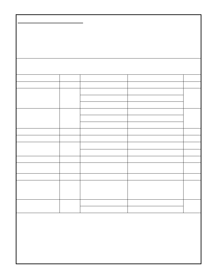
∑ 2.048 V Output ± 0.205 mV (.01%)
∑ Temperature Drift: 0.6 ppm/∞C
∑ Low Noise: 1.5
µ
V
p-p
(0.1Hz-10Hz)
∑ Low Thermal Hysteresis: 1 ppm Typ.
∑ ±15mA Output Source and Sink Current
∑ Excellent Line Regulation: 5 ppm/V Typ.
∑ Optional Noise Reduction and Voltage Trim
∑ Industry Standard Pinout
FIGURE 1
SELECTION GUIDE
Model
Temp.
Range ∞C
Temp.
Coeff.
ppm/∞C
VRE3021A
0.205
0.6
0∞C to +70∞C
VRE3021B
0.307
1.0
0∞C to +70∞C
VRE3021C
0.410
2.0
0∞C to +70∞C
VRE3021J
0.205
0.6
-40∞C to +85∞C
VRE3021K
0.307
1.0
-40∞C to +85∞C
VRE3021L
0.410
2.0
-40∞C to +85∞C
For package option add D for DIP or S for Surface Mount
to end of model number.
Initial
Error
mV
THALER CORPORATION ∑ 2015 N. FORBES BOULEVARD ∑ TUCSON, AZ. 85745 ∑ (520) 882-4000
N/C
VRE3021
Low Cost
Precision Reference
VRE3021DS REV. D JULY 2000
ppm/
1khrs
6
V
OUT/t
Long Term Stability
µ
Vp-p
1.25
0.1Hz<f<1kHz
e
n
Output Noise Voltage
µ
s
2
To 0.01% of final value
T
on
Turn-On Settling Time
mV
±2
Figure 3
V
OUT
Trim Adjustment Range
1.0 2.0
VRE3025C/K
0.5 1.0
VRE3025B/K
2.0476 2.048 2.0484
VRE3025C/L
2.0477 2.048 2.0483
VRE3025B/K
V
2.0478 2.048 2.0482
VRE3025A/J
V
OUT
Output Voltage
(Note 1)
5 10
10V
V
IN
18V
ppm/V
25 35
8V
V
IN
10V
V
OUT
/
V
IN
Line Regulation
ppm/
mA
8 12
8 12
Sourcing:
0mA
I
OUT
15mA
Sinking:
-15mA
I
OUT
0mA
V
OUT
/
I
OUT
Load Regulation
mA
3.5 4.0
I
IN
Supply Current
µ
V
RMS
1.25 2.5
10Hz<f<1Hz
ppm
1
Note 4
Temperature Hysterisis
ppm/∞C
0.3 0.6
VRE3025A/J
TCV
OUT
Output Voltage
Temperature Coefficient
(Note 2)
V
8 36
V
IN
UNITS
MIN
TYP
MAX
SYMBOL
CONDITIONS
Input Voltage
PARAMETER
ELECTRICAL SPECIFICATIONS
Vps =+10V, T = 25∞C, Iout=0mA unless otherwise noted.
ABSOLUTE MAXIMUM RATINGS
Power Supply ...........................-0.3V to +40V
Out Short Circuit to GND Duration (V
IN
< 12V)......Continuous
OUT, TRIM ..............................-0.3V to +12V
Out Short Circuit to GND Duration (V
IN
< 40V)..............5 sec
NR..........................................-0.3V to +6V
Out Short Circuit to IN Duration (V
IN
< 12V)..........Continuous
Operating Temp. (
A,B,C
)...............0 ∞C to 70∞C
Continuous Power Dissipation (T
A
= +70∞C).............300mW
Operating Temp. (
J,K,L
)...............-40 ∞C to 85∞C
Storage Temperature.................................-65∞C to 150∞C
Lead Temperature (soldering,10 sec) .......................250∞C
VRE3021DS REV. D JULY 2000
Notes:
1) The specified values are without external trim.
2) The temperature coefficient is determined by the
box method. See discussion on temperature
performance.
3) Line and load regulation are measured with pulses and
do not include voltage changes due to temperature.
4) Hysterisis over the operating temperature range.
TYPICAL PERFORMANCE CURVES
Temperature (
o
C)
VRE3025A
V
OUT
vs. TEMPERATURE
SUPPLY CURRENT
VS. SUPPLY VOLTAGE
QUIESCENT CURRENT VS. TEMP
Temperature (
o
C)
OUTPUT IMPEDIANCE
VS. FREQUENCY
Temperature (
o
C)
VRE3025B
V
OUT
vs. TEMPERATURE
V
OUT
vs. TEMPERATURE
Temperature (
o
C)
VRE3025C
Temperature (
o
C)
VRE3025J
V
OUT
vs. TEMPERATURE
Temperature (
o
C)
VRE3025K
V
OUT
vs. TEMPERATURE
Temperature (
o
C)
VRE3025L
V
OUT
vs. TEMPERATURE
Supply Voltage (V)
Supply Current (mA)
Frequency (Hz)
V
out
(mV)
V
out
(mV)
V
out
(mV)
V
out
(mV)
V
out
(mV)
V
out
(mV)
Quiescent Current (mA)
Output
Impediance
(
)
VRE3021DS REV. D JULY 2000
0
50
-50
100
6.0
4.0
2.0
0
8.0
15
25
5
35
5.0
4.0
3.0
0
6.0
10
20
30
40
0
-50 -25
0
25 50 75 100
2.0
1.5
1.0
0.5
0
-1.0
-0.5
-1.5
-2.0
Lower Limit
Upper Limit
-50 -25
0
25 50 75 100
2.0
1.5
1.0
0.5
0
-1.0
-0.5
-1.5
-2.0
Lower Limit
Upper Limit
0 20 30 40 50 60 70
1.00
0.75
0.50
0.25
0
-0.50
-0.25
-0.75
-1.00
Lower Limit
Upper Limit
0 20 30 40 50 60 70
1.00
0.75
0.50
0.25
0
-0.50
-0.25
-0.75
-1.00
Lower Limit
Upper Limit
Lower Limit
Upper Limit
-0.75
0 20 30 40 50 60 70
1.00
0.75
0.50
0.25
0
-0.50
-0.25
-1.00
Lower Limit
Upper Limit
-50 -25
0
25 50 75 100
2.0
1.5
1.0
0.5
0
-1.0
-0.5
-1.5
-2.0
Lower Limit
Upper Limit
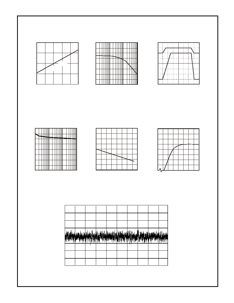
TYPICAL PERFORMANCE CURVES
RIPPLE REJECTION
Vs. FREQUENCY(C
NR
=0
µ
F)
OUTPUT NOISE-VOLTAGE
DENSITY vs. FREQUENCY
VRE3021DS REV. D JULY 2000
JUNCTION TEMP. RISE VS.
OUTPUT CURRENT
Output Current (mA)
CHANGE IN OUTPUT VOLTAGE
VS. INPUT VOLTAGE
CHANGE IN OUTPUT VOLTAGE
VS. OUTPUT CURRENT
V
in
(V)
Vout (ppm)
I
out
(mA)
Vout (
µ
V)
Frequency (Hz)
Frequency (Hz)
1k
10k
90
80
70
60
100
100
10
0
4
2
8
6
10
30
20
10
0
40
Vcc
=
1
0V
12 13
9
15
20
0
-20
14
16
11
10
0
-10
10
30
40
50
60
Ripple Rejection (dB)
Junction Temperature
Rise Above Ambient (
o
C)
Output Noise Density (
nV
/
Hz)
8 10
2
14
0
-200
-400
12
16
6
4
0
-300
-100
100
200
300
400
TURN-ON AND TURN-OFF
TRANSIENT RESPONSE
1
µ
s/div
B
A
0V
+10V
A: Vin, 10V/div
B: Vout, 1V/div
1k
10k
40
30
20
10
50
100
10
0.1Hz to 10Hz Noise
Vout, 0.5
µ
V/Div
1 Sec/Div
VRE3021DS REV. D JULY 2000
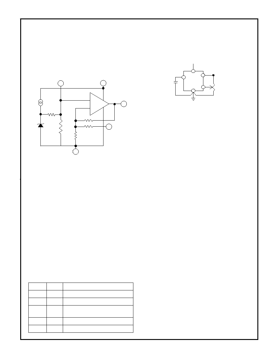
THEORY OF OPERATION
The following discussion refers to the schematic in
figure 2 below. A FET current source is used to bias a
6.3V zener diode. The zener voltage is divided by the
resistor network R1 and R2. This voltage is then applied
to the noninverting input of the operational amplifier which
amplifies the voltage to produce a 2.048V output. The
gain is determined by the resistor networks R3 and R4:
G=1 + R4/R3. The 6.3V zener diode is used because it is
the most stable diode over time and temperature.
The current source provides a closely regulated zener
current, which determines the slope of the references'
voltage vs. temperature function. By trimming the zener
current a lower drift over temperature can be achieved.
But since the voltage vs. temperature function is nonlinear
this compensation technique is not well suited for wide
temperature ranges.
Thaler Corporation has developed a nonlinear
compensation network of thermistors and resistors that is
used in the VRE series voltage references. This
proprietary network eliminates most of the nonlinearity in
the voltage vs. temperature function. By adjusting the
slope, Thaler Corporation produces a very stable voltage
over wide temperature ranges.
This network is less than 2% of the overall network
resistance so it has a negligible effect on long term
stability. Figure 3 shows the proper connection of the
VRE3021 series voltage references with the optional trim
resistor for initial error and the optional capacitor for noise
reduction.
BASIC CIRCUIT CONNECTION
Figure 3 shows the proper connection of the VRE3025
voltage reference with the optional trim resistor for initial
error and optional capacitor for noise reduction.
To achieve the specified performance, pay careful
attention to the layout. A low resistance star configuration
will reduce voltage errors, noise pickup, and noise
coupled from the power supply. Commons should be
connected to a single point to minimize interconnect
resistances.
Figure 3 External Connections
6
Figure 2 Functional Block Diagram
8
5
2
4
R1
R2
R3
R4
+
-
Noise Reduction
NR
8
Voltage reference output
OUT
6
External trim input. Leave open if
not used.
TRIM
5
Ground
GND
4
Positive power supply input
Internally connected. Do not use
Vin
N.C.
2
1,3,7
PIN DESCRIPTION
8
6
5
+ V
OUT
2
+ V
IN
4
VRE3021
10k
C
N
1µF
Optional Noise
Reduction
Capacitor
Optional Fine
Trim Adjustment