 | –≠–ª–µ–∫—Ç—Ä–æ–Ω–Ω—ã–π –∫–æ–º–ø–æ–Ω–µ–Ω—Ç: THAT1200S | –°–∫–∞—á–∞—Ç—å:  PDF PDF  ZIP ZIP |
THAT Corporation; 45 Sumner Street; Milford, Massachusetts 01757-1656; USA
Tel: +1 (508) 478-9200; Fax: +1 (508) 478-0990; Web: www.thatcorp.com
THAT 1200, 1203, 1206
Description
The THAT 1200 series of InGenius balanced
line receivers are designed to overcome a serious
limitation of conventional balanced input stages
-- notoriously poor common mode rejection in
real world applications. While conventional input
stages may exhibit good rejection characteristics
in the lab and on paper, they perform poorly
when fed from even slightly unbalanced source
impedances -- a common situation in almost any
pro sound environment.
Developed by Bill Whitlock of Jensen Trans-
formers, the patented InGenius input stage uses a
unique bootstrap circuit to raise its common-
mode input impedance into the megohm range,
but without the noise penalty that comes from
high-valued resistors. InGenius line receivers
maintain their high CMRR over a wide range of
source impedance imbalances -- even when fed
from single-ended sources.
T H A T
C o r p o r a t i o n
InGenius
‚
High-CMRR
Balanced Input Line Receiver
FEATURES
∑
High common-mode rejection
(typical 90 dB at 60 Hz) maintained
under real-world conditions
∑
Excellent solution for hum and
groundloop suppression
∑
Transformer-like noise rejection in
an 8-pin IC, at fraction of
transformer cost and size
APPLICATIONS
∑
Balanced input stages
∑
Summing amplifiers
∑
Transformer front-end
replacements
∑
ADC front-ends
+1
+1
R1
R2
R3
R4
IN-
IN+
REF
CM OUT
Vcc
Vee
Vout
+1
-
+
CM IN
Cb
R5
Ra
Rb
Rc
Rd
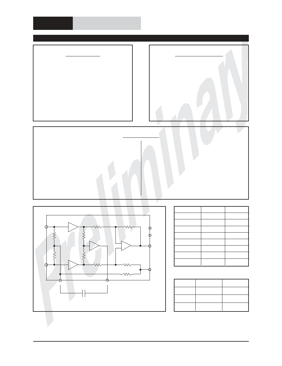
OA1
OA2
OA3
OA4
Figure 1. THAT1200-series equivalent circuit diagram
Pin Name
DIP Pin
SO Pin
Ref
1
3
In-
2
4
In+
3
5
Vee
4
6
CM In
5
11
Vout
6
12
Vcc
7
13
CM Out
8
14
Table 1. 1200-series pin assignments
Gain
Plastic DIP
Plastic SO
0 dB
1200P
1200S
-3 dB
1203P
1203S
-6 dB
1206P
1206S
Table 2. Ordering information
Protected under U.S. Patent No. 5,568,561 and other patents pending.
InGenius‚ is a trademark of THAT Corporation.
600033 Rev 0A

THAT Corporation; 45 Sumner Street; Milford, Massachusetts 01757-1656; USA
Tel: +1 (508) 478-9200; Fax: +1 (508) 478-0990; Web: www.thatcorp.com
Page 2
InGenius Balanced Line Receiver
Preliminary Information
Absolute Maximum Ratings (T
A
= 25∞C)
Positive Supply Voltage (V
CC
)
+18 V
Power Dissipation (P
D
) (T
A
= 75∞C)
TBD mW
Negative Supply Voltage (V
EE
)
-18 V
Operating Temperature Range (T
OP
)
0 to +70∞C
Positive Input Voltage (V
IN+
)
+18 V
Storage Temperature Range (T
ST
)
-40 to +125∞C
Negative Input Voltage (V
IN-
)
-18 V
Junction Temperature (T
J
)
150∞C
Output Short-Circuit Duration (t
SH
)
Continuous
Lead Temperature (Soldering 60 seconds)
TBD ∞C
Electrical Characteristics
2
Parameter
Symbol
Conditions
Min
Typ
Max
Units
Supply Current
I
CC
No signal
--
4.7
8.0
mA
Input Bias Current
I
B
No signal; Either input
--
700
1,400
nA
connected to GND
Input Offset Current
I
B-OFF
No signal
--
--
±140
nA
Input Offset Voltage
V
OFF
No signal
--
--
10
mV
Input Voltage Range
V
IN-CM
Common mode
±12.5
±13.0
--
V
V
IN-DIFF
Differential (equal and opposite swing)
THAT 1200
21.0
21.5
--
dBu
THAT 1203
24.0
24.5
--
dBu
THAT 1206
24.0
24.5
--
dBu
Input Impedance
Z
IN-DIFF
Differential
48.0
k
W
Z
IN-CM
Common mode
with bootstrap
60 Hz
10.0
M
W
20 kHz
3.2
M
W
no bootstrap
60 Hz
36.0
k
W
20 kHz
36.0
k
W
Recommended Operating Conditions
Parameter
Symbol
Conditions
Min
Typ
Max
Units
Positive Supply Voltage
V
CC
+3
+18
V
Negative Supply Voltage
V
EE
-3
-18
V
SPECIFICATIONS
1
1. All specifications are subject to change without notice.
2. Unless otherwise noted, T
A
=25∞C, V
CC
= +15V, V
EE
= -15V
3. 0 dBu = 0.775Vrms.

THAT Corporation; 45 Sumner Street; Milford, Massachusetts 01757-1656; USA
Tel: +1 (508) 478-9200; Fax: +1 (508) 478-0990; Web: www.thatcorp.com
600033 Rev 0A
Page 3
Preliminary Information
Electrical Characteristics (Cont'd)
Parameter
Symbol
Conditions
Min
Typ
Max
Units
Common Mode Rejection
CMR
1
Matched source impedances; V
CM
= ±10V
DC
70
90
--
dB
60 Hz
70
90
--
dB
20 kHz
--
85
--
dB
Common Mode Rejection
CMR
2
600
W unmatched source impedances
4
; V
CM
= ±10V
60 Hz
--
70
--
dB
20 kHz
--
65
--
dB
Power Supply Rejection
5
PSR
At 60 Hz, with V
CC
= -V
EE
THAT1200
--
82
--
dB
THAT1203
--
80
--
dB
THAT1206
--
80
--
dB
Power Supply Rejection
6
PSR
CM
At CM output, at 60 Hz
--
63
--
dB
Total Harmonic Distortion
THD
V
IN-DIFF
= 10 dBV; BW = 20 kHz; f = 1 kHz
RL =2 k
W
--
0.0005
--
%
Output Noise
e
n(OUT)
BW = 20 kHz
THAT1200
--
-106
--
dBu
THAT1203
--
-105
--
dBu
THAT1206
--
-107
--
dBu
Output Noise
e
nCM(OUT)
At CM output
--
-106
--
dBu
Slew Rate
SR
R
L
= 10 k
W; C
L
= 300 pF
7*
12
--
V/µs
Slew Rate
SR
CM
With CM input signal
12.5*
21
--
V/µs
R
Lcm
= 10 k
W; C
Lcm
= 50 pF
Small Signal Bandwidth
BW
-3dB
R
L
= 10 k
W; C
L
= 10 pF
THAT1200
--
22
--
MHz
THAT1203
--
27
--
MHz
THAT1206
--
34
--
MHz
R
L
= 2 k
W; C
L
= 300 pF
THAT1200
--
17
--
MHz
THAT1203
--
18
--
MHz
THAT1206
--
20
--
MHz
Small Signal Bandwidth
BW
CM-3dB
At CM output; R
Lcm
= 10 k
W
C
Lcm
= 10 pF
--
20
--
MHz
C
Lcm
= 50 pF
--
18
--
MHz
Output Gain Error
G
ER(OUT)
f = 1 kHz; R
L
= 2 k
W
--
0
±0.05
dB
Output Voltage Swing
V
O
At max differential input
THAT1200
21
21.5
--
dBu
THAT1203
21
21.5
--
dBu
THAT1206
18
18.5
--
dBu
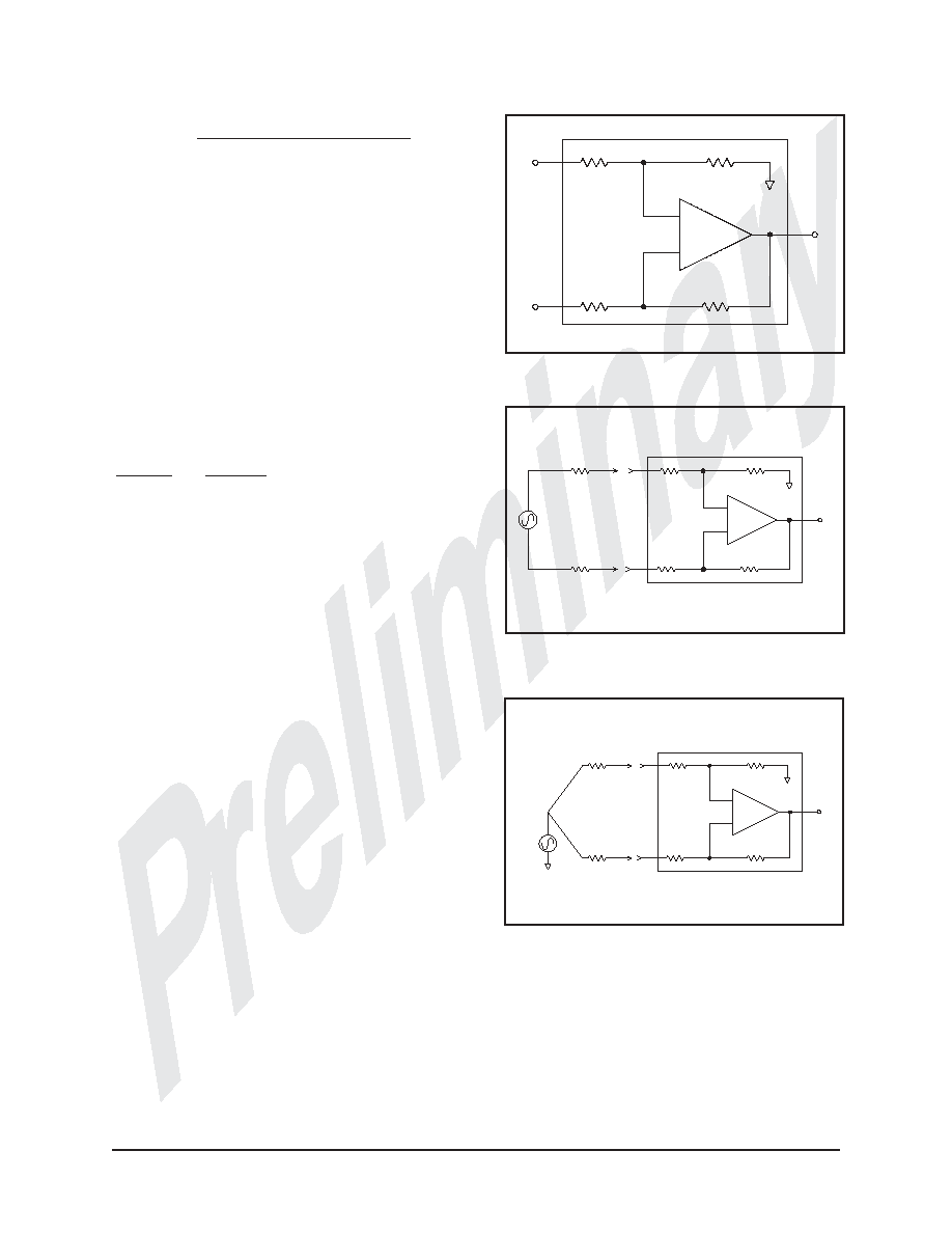
4. See test circuit in Figure 2.
5. Defined with respect to the differential gain.
6. Defined with respect to the common mode gain between any input and common mode output.
* Guaranteed by design
Applications
RFI Protection
Figure 3 shows the THAT 1200 configured with
robust RFI input protection.
In applications where
RFI rejection is of less concern, the circuit shown Fig-
ure 4 provides a less aggressive approach.
Bootstrap coupling capacitor
Referring to Figure 3, electrolytic capacitor Cb
provides the feedback path for the boostrap circuit.
The capacitor value is chosen to be high enough to
present a sufficiently small impedance to signals at
the low end of the audio spectrum. Its voltage rating
is dependent on the topology of the surrounding cir-
cuitry, as described in the following paragraphs.
AC signals presented to the input stage cause the
two ends of capacitor Cb to swing in tandem so that
virtually no voltage appears across the capacitor.
Consequently, capacitors with small DC working volt-
ages may be used when the previous stage is AC cou-
pled to the input of the THAT 1200.
THAT Corporation; 45 Sumner Street; Milford, Massachusetts 01757-1656; USA
Tel: +1 (508) 478-9200; Fax: +1 (508) 478-0990; Web: www.thatcorp.com
Page 4
InGenius Balanced Line Receiver
Preliminary Information
Electrical Characteristics (Cont'd)
Parameter
Symbol
Conditions
Min
Typ
Max
Units
Output Short Circuit Current
I
SC
R
L
= R
Lcm
= 0
W
--
±25
--
mA
I
CMSC
At CM output
--
±10
--
mA
Minimum Resistive Load
R
Lmin
2
--
--
k
W
R
LCMmin
At CM output
10
--
--
k
W
Maximum Capacitive Load
C
Lmax
--
--
300
pF
C
LCMmax
At CM output
--
--
50
pF
1
In-
2
In+
3
CMin
5
4
8
7
Out
6
U1
THAT120x
Cb
100u
C1
56p
C2
300p
C3
100n
C4
100n
R1
200k
R2
200k
R3
600R
R4
2k
R5
100R
R6
100R
Vcc
Vee
In-
In+
Ext. DC Source
CM Out
Main Out
Gnd
Gnd
Gnd
CMout
Vcc
Ref
Vee
Figure 2. THAT1200-series test circuit
If, however, there is the possibility of a DC voltage
appearing across the inputs of the line receiver, a
portion of that voltage will appear directly across the
terminals of capacitor Cb. In that case, choose the
capacitor's voltage rating so that it is capable of han-
dling the expected level of DC voltage. If the polarity
of the DC voltage is unknown, or may swing to either
polarity, the use of a non-polarized electolytic is
highly recommended.
THAT Corporation; 45 Sumner Street; Milford, Massachusetts 01757-1656; USA
Tel: +1 (508) 478-9200; Fax: +1 (508) 478-0990; Web: www.thatcorp.com
600033 Rev 0A
Page 5
Preliminary Information
5
IN-
2
IN+
3
8
4
1
7
6
OUT
CM
IN
CM
OUT
REF
VCC
VEE
U1
Cb
220uF
5 4
3 1
2
2
3
1
J1
XLR-F
Vcc
Vee
OUT
C2
100pF NPO
C1
100pF NPO
+
Vcc
Vee
D1
12V
D2
12V
D4
D3
D6
D5
Figure 4. THAT1200P showing simplified RFI protection scheme
5
IN-
2
IN+
3
8
4
1
7
6
OUT
CM
IN
CM
OUT
REF
VCC
VEE
U1
R3
4k7
Cb
220uF
C2
470pF
C3
470pF
C4
100pF
R1
R2
5 4 3 1
2
2
3
1
J1
XLR-F
Vcc
Vee
OUT
100R
100R
(see text)
optional RFI protection
+
Vcc
Vee
D1
12V
D2
12V
D4
D3
D6
D5
Figure 3. THAT1200P typical application circuit
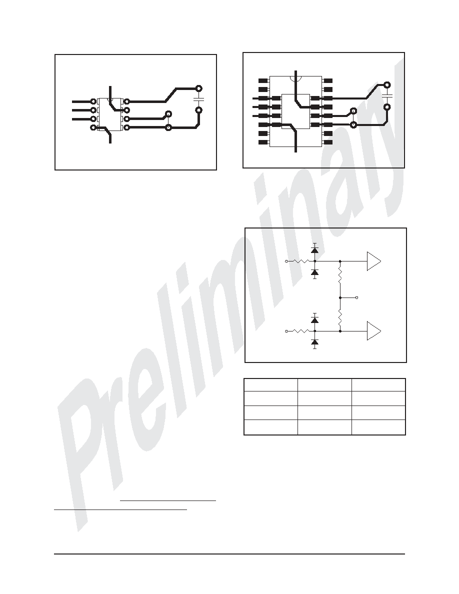
Dual Layout Option
The THAT 1246 is a conventional balanced
line-receiver that is pin-for-pin compatible with the
Analog Devices SSM2143 and Burr-Brown INA137.
Though the THAT 1200 series is not pin-compatible
with the THAT 1246, the PCB layouts shown in Fig-
ures 5 and 6 provide manufacturers with the option
to stuff a PCB with any of these input stages. Note
that these figures are not to scale. The interconnects
should be as short as practicable constrained only by
component size and relevant manufacturing consid-
erations.
When a THAT 1200 series IC is installed, capaci-
tor Cb is connected between CM In and CM Out.
When the THAT 1246 (or SSM2143 or INA137) is
used, capacitor Cb is removed, and a jumper con-
nects the Vout and Sense pins.
Input Protection
Figure 7 shows the internal overvoltage protection
circuitry at the IN+, IN-, and CM IN pins. The values
of R and R' vary with actual part number as shown in
Table 3.
While the internal protection circuitry shown is
adequate to keep the combination of signal and com-
mon mode voltages from driving the internal inputs
beyond the power supply rails, the circuitry does not
provide adequate protection against most ESD inci-
dents. Since these ICs will very often connect directly
to the outside world, it is mandatory that additional,
external protection from ESD be provided. Any un-
protected InGenius input will fail when subjected to
ESD if this protection circuitry is omitted.
Addi-
tionally, proper ESD handling precautions must be
observed until the IC is properly affixed to the PCB.
Diodes D1-D6 in figures 3 and 4 show our recom-
mended approach to protecting the 1200 series from
ESD damage.
This arrangement of 1N4148s and
12V Zener diodes permits the maximum allowable
input signal to reach the IC's input pins, but directs
high-energy ESD impulses to the rails. So long as the
supply rails are adequately decoupled, most ESD
events will be diminished to harmless levels.
THAT Corporation; 45 Sumner Street; Milford, Massachusetts 01757-1656; USA
Tel: +1 (508) 478-9200; Fax: +1 (508) 478-0990; Web: www.thatcorp.com
Page 6
InGenius Balanced Line Receiver
Preliminary Information
R
R
R'
R'
Vcc
Vcc
Vee
IN+
IN-
CM IN
Vee
Figure 7. Internal input protection circuitry (see text)
Part No.
R
R'
THAT 1200
500
W
23.5k
W
THAT 1203
7k
W
17k
W
THAT 1206
7k
W
17k
W
Table 3. Input resistance values
Vcc
Gnd
In-
In+
Vee
CM out or N/C
Vcc
Vout
CM in or Sense
Connect
for
THAT1246
Ref
In-
In+
Vee
Cb
THAT1206
or THAT1246
+
Figure 5. Dual PCB layout for THAT 1206 and THAT 1246
DIP version
Vcc
Gnd
In-
In+
Vee
CM Out
Vcc
Vout
CM in
Connect
for
THAT1246
Ref
In-
In+
Vee
Cb
THAT1246
THAT1206
N/C
Vout
Sense
Vee
Vcc
+
Figure 6. Dual PCB layout for THAT 1206 and THAT 1246
Surface mount versions
Theory of Operation
Conventional high-CMRR balanced input stages
cancel common-mode interference using a differential
amplifier with matched (trimmed) resistance ele-
ments (Figure 8). When driven from a true voltage
source, these conventional stages offer extremely high
CMRR (>80dB).
However, when driven from real-
world sources, the CMRR of these stages degrades
rapidly for even small source impedance imbalances.
The reason why this occurs is easily shown. Fig-
ure 9 shows that a voltage divider is formed between
the impedance of the external signal source and the
input impedance of the differential amplifier.
For
perfectly balanced source impedances (Rs1 = Rs2),
and
perfectly
balanced
input
impedances
(Ri1 = Ri2), the voltage dividers formed at each node
(
Ri
Ri
Rs
1
1
1
+
and
Rs
Ri
Rs
2
2
2
+
) will be equal to each other,
so the conventional input stage will maintain high
CMRR.
However, if the source impedances are not pre-
cisely equal, the voltage divider action will result in
unequal signals at the plus and minus inputs of the
input stage. In this case, no amount of CMRR is suf-
ficient to reject the differential voltage that is gener-
ated by the impedance mismatch.
To illustrate, consider Figure 10.
A common
mode input signal is shown as Vcm. It couples to the
positive and negative input of the balanced line re-
ceiver via Rs1 and Rs2, repectively.
Typically, con-
ventional balanced line receivers have common-mode
input impedances of approximately 10 k
W. In such
cases, a source impedance imbalance of only 10
W
can degrade CMRR to about 65 dB.
A 10
W mis-
match may be easily caused by tolerances in coupling
capacitors or output resistors, and variations in con-
tact and wire resistance. The situation becomes even
worse when a conventional balanced line receiver is
driven from an unbalanced source.
The best solution to this problem is to increase
the line receiver's common-mode input impedance
enough to minimize the imbalanced voltage divider
effect, preferably on the order of several megohms.
However, with a conventional differential amplifier,
this requires the use of high resistances in the cir-
cuit. High resistance carries with it a high noise pen-
alty,
making
this
straightforward
approach
impractical for quality audio devices.
An alternative approach is to use the classic in-
strumentation amplifier configuration shown in Fig-
ure 11.
In this circuit, the common-mode input
impedance is the parallel combination of Ri1 and
Ri2.
Unfortunately for this approach, to achieve
multi-megohm input impedances, the input devices
used in the input amplifiers must have extremely low
THAT Corporation; 45 Sumner Street; Milford, Massachusetts 01757-1656; USA
Tel: +1 (508) 478-9200; Fax: +1 (508) 478-0990; Web: www.thatcorp.com
600033 Rev 0A
Page 7
Preliminary Information
+
-
Rs1
Rs2
Rs1 Rs2
π
Vout
+Vin
-Vin
Ri1
Ri2
Vcm
Figure 10. Basic differential amplifier driven
by common-mode input signal
Rs1
Rs2
Rs1
s2
πR
+
-
Vout
+Vin
-Vin
Ri1
Ri2
Figure 9. Basic differential amplifier showing
mismatched source impedances
+
-
Vout
+Vin
-Vin
Ri1
Ri2
Figure 8. Basic differential amplifier

bias currents since their input bias flows through Ri1
and Ri2. Because of the difficulty of maintaining low
noise with low input bias currents, FET op amps
may be employed, but they impose their own limita-
tions, as described further on.
The THAT 1200 series of balanced line receivers
overcomes this problem by way of an AC bootstrap
technique, shown in simplified form in Figure 12. By
driving the lower end of R2 to nearly the same AC
voltage as the upper end, AC current flow through R2
is greatly reduced, effectively increasing its value. At
DC, of course, the input impedance Z is simply R1 +
R2.
If gain G is unity, for frequencies within the
passband of the high-pass filter formed by Cb and
R1, the effective value of the input impedance is in-
creased to infinity at sufficiently high frequencies.
Input impedance Z, at frequency f, is described
the following equation:
Z
R
R
G
i
f
fn
f
fD
=
+
+
+ -
(
)
(
)
(
) (
)
1
2
2
2
2
1
1
1
where
f
C
f
R C
N
R
R
R
R
D
=
=
¥
+
1
2
1
2
1
2
1
2
1
p
p
(
)
,
For example, if R1 and R2 are 10 k
W each, Z
DC
is
20 k
W. This resistance provides a DC path for am-
plifier bias current as well as leakage current that
might flow from a signal source. At higher frequen-
cies, the bootstrap greatly increases the input imped-
ance,
limited
ultimately
by
how
close
gain
G
approaches unity. With the THAT 1200 input stages,
common-mode input impedances of several meg-
ohms across much of the audio spectrum can be ex-
pected.
Figure 1 shows a complete equivalent circuit for
the THAT 1200-series ICs.
OA1 and OA2 are
high-impedance buffers feeding differential amplifier
OA3 in an instrumentation amplifier configuration.
The common mode signal is extracted at the junction
of Rc and Rd, buffered by OA4, and fed back to both
inputs via capacitor Cb and resistors Ra and Rb.
The junction of Ra, Rb and R5 is driven to the same
potential as the common-mode input voltage. Hence
no common-mode current flows in resistors Ra and
Rb. Since, ideally, no current flows, the input imped-
ance to common mode signals is infinite.
The effectiveness of this topology is limited by the
unity gain precision of OA4 and the input imped-
ances of OA1 and OA2, all of which are optimized in
THAT's integrated circuit process.
Note that OA1
and OA2 isolate OA3 from external source imped-
ances. Therefore, the performance of the differential
amplifier OA3 and its associated components are not
affected by imbalances in the source impedances.
Alternatives
In the following section we will compare other so-
lutions for minimizing CMRR degradation in the
presence of source impedance mismatch, and con-
trast them with THAT's InGenius topology.
Precision 4-resistor op amp stage
This stage (Figure 8) was discussed earlier.
To
summarize, this solution offers high common-mode
rejection only when the source impedances are per-
fectly balanced, or a tiny fraction of the common-
mode input impedance.
Because differential- and
THAT Corporation; 45 Sumner Street; Milford, Massachusetts 01757-1656; USA
Tel: +1 (508) 478-9200; Fax: +1 (508) 478-0990; Web: www.thatcorp.com
Page 8
InGenius Balanced Line Receiver
Preliminary Information
Z
R2
R1
G = 1
Cb
Figure 12. InGenius bootstrap topology
Out
+ In
- In
+
-
+
-
+
-
OA1
OA2
OA3
Ri1
Ri2
Figure 11. Instrumentation amplifier

common-mode input impedances are inextricably
linked, and of similar magnitude, it is not possible to
increase common-mode input impedance without
compromising noise performance.
3-op amp instrumentation amplifier
This topology, shown in Figure 11, was also dis-
cussed earlier.
It relies on input buffers OA1 and
OA2 to raise the common-mode and differential-
mode input impedances.
The following diff amp,
OA3 (which can be of the precision 4-resistor op amp
type), is then used to reject the common-mode signal
while extracting the differential signal.
This approach will require reasonably low values
for Ri1 and Ri2 (< 100 k
W or so) unless the OA1 and
OA2 use FETs at their inputs. This would limit the
common-mode input impedance to a few hundred
kilohms.
If FET-input devices are used for OA1 and OA2,
Ri1 and Ri2 can be made quite large -- on the order
of 10 megohms. Unlike the resistors in the conven-
tional diff amp stage, these resistors will be shunted
by the driving source impedance, and so contribute
negligible noise.
At first glance, this might seem to be an excellent
solution.
However, there are disadvantages to this
approach.
First, the designer must select a FET-
input op amp that is low-noise and that exhibits no
phase inversion (sign reversal) with large differential-
and common-mode signal swings.
This, of course,
results in a cost penalty that is somewhat exacer-
bated by the price premium for high-value resistors.
Second, this design requires at least two IC pack-
ages -- a dual FET op amp and the precision input
stage.
Third, while the large-value input resistances are
shunted when there is a source connected to the
input, there is no guarantee that long cables will al-
ways be properly terminated. With an unterminated
cable plugged into the associated XLR jack, Ri1 and
Ri2 are no longer shunted and become not only large
noise sources themselves, but will do little to reduce
pickup on the cable.
The THAT 1200-series input stages avoid these
problems altogether.
They exhibit high common-
mode input impedance as a result of their boot-
strapped topology, while maintaining reasonable dif-
ferential input resistances that can be left unshunted
with no fear of stray pickup or excessive noise contri-
bution.
Transformers
When true electrical isolation is required, a trans-
former may be the only solution. Transformers suit-
able for pro audio, however, tend to be costly and
take up valuable board real estate. In addition, some
transformers can color the sound in ways that elec-
tronic solutions do not.
Fortunately, it is usually not the case that galvanic
isolation is required, and in most cases it is the
common-mode signal rejection properties of a trans-
former that is sought after.
By providing the high
common-mode input impedance of a transformer
with the size and cost of an 8-pin integrated circuit,
the THAT 1200-series provides designers with an al-
ternative that provides excellent interference rejection
in real-world applications.
THAT Corporation; 45 Sumner Street; Milford, Massachusetts 01757-1656; USA
Tel: +1 (508) 478-9200; Fax: +1 (508) 478-0990; Web: www.thatcorp.com
600033 Rev 0A
Page 9
Preliminary Information
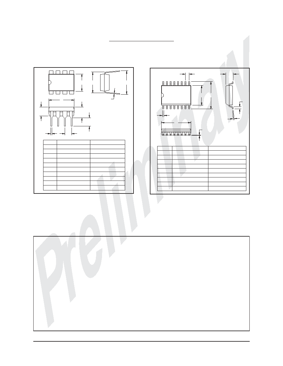
Package Information
The THAT 1200 series is available in both 8-pin
mini-DIP and 16-pin SOIC packages.
The package
dimensions are shown in Figures 13 and 14, while
pinouts are given in Table 1.
THAT Corporation; 45 Sumner Street; Milford, Massachusetts 01757-1656; USA
Tel: +1 (508) 478-9200; Fax: +1 (508) 478-0990; Web: www.thatcorp.com
Page 10
InGenius Balanced Line Receiver
Preliminary Information
D
E
B
C
J
A
F
H
G
1
ITEM
A
B
C
D
E
F
G
H
J
MILLIMETERS
10.11/10.31
7.40/7.60
10.11/10.51
0.36/0.46
1.27
2.44/2.64
0.23/0.32
0.51/1.01
0.10/0.30
INCHES
0.398/O.406
0.291/0.299
0.398/0.414
0.014/0.018
0.050
0.096/0.104
0.009/0.013
0.020/0.040
0.004/0.012
Figure 14. -S (SO) version package outline drawing
B
A
K
F
H
E
D
G
J
C
ITEM
A
B
C
D
E
F
G
H
J
K
1
MILLIMETERS
9.52 0.10
6.35 0.10
7.49/8.13
0.46
2.54
3.68/4.32
0.25
3.18 0.10
8.13/9.40
3.30 0.10
±
±
±
±
INCHES
0.375
0.250 0.004
0.295/0.320
0.018
0.100
0.145/0.170
0.010
0.125 0.004
0.320/0.370
0.130 0.004
±0.004
±
±
±
Figure 13. -P (DIP) version package outline drawing
Information furnished by THAT Corporation is believed to be accurate and reliable. However no responsibil-
ity is assumed by THAT Corporation for its use nor for any infringements of patents or other rights of third par-
ties which may result from its use.
LIFE SUPPORT POLICY
THAT Corporation products are not designed for use in life support equipment where malfunction of such
products can reasonably be expected to result in personal injury or death. The buyer uses or sells such prod-
ucts for life suport application at the buyer's own risk and agrees to hold harmless THAT Corporation from all
damages, claims, suits or expense resulting from such use.
CAUTION: THIS IS AN ESD (ELECTROSTATIC DISCHARGE) SENSITIVE DEVICE.
It can be damaged by the currents generated by electrostatic discharge. Static charge and therefore danger-
ous voltages can accumulate and discharge without detection causing a loss of function or performance to occur.
The transistors in this device are unprotected in order to maximize performance and flexibility. They are
more sensitive to ESD damage than many other ICs which include protection devices at their inputs.
Use ESD preventative measures when storing and handling this device. Unused devices should be stored in
conductive packaging. Packaging should be discharged before the devices are removed. ESD damage can occur
to these devices even after they are installed in a board-level assembly. Circuits should include specific and ap-
propriate ESD protection.