 | –≠–ª–µ–∫—Ç—Ä–æ–Ω–Ω—ã–π –∫–æ–º–ø–æ–Ω–µ–Ω—Ç: THAT 140 | –°–∫–∞—á–∞—Ç—å:  PDF PDF  ZIP ZIP |
THAT Corporation; 45 Sumner St., Milford, Massachusetts; 01757-1656; USA
Tel: +1 (508) 478-9200; Fax: +1 (508) 478-0990; Web: www.thatcorp.com
T H A T
C o r p o r a t i o n
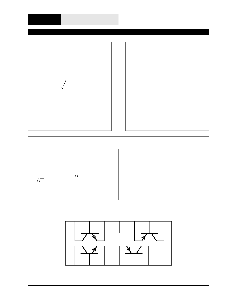
1
2
3
4
5
6
7
SUB
NC
8
9
10
11
12
13
14
Q2
Q1
Q4
Q3
Figure 1. Pin Configuration
Quad Low-Noise
NPN / PNP Transistor Array
THAT140
FEATURES
∑
Two Matched NPN Transistors
Two Matched PNP Transistors
∑
Monolithic Construction
∑
Low Noise
-- 0.75
nV
/ Hz (PNP)
-- 0.8
nV
/ Hz (NPN)
∑
High Speed
-- f
t
= 350 MHz (NPN)
-- f
t
= 325 MHz (PNP)
∑
Excellent Matching - 500 mV typ
∑
Dielectrically Isolated
∑
25 V V
CEO
APPLICATIONS
∑
Microphone Preamplifiers
∑
Tape Head Preamplifiers
∑
Current Sources
∑
Current Mirrors
∑
Log/Antilog Amplifiers
∑
Multipliers
DESCRIPTION
THAT140 is a quad, large-geometry monolithic
NPN/PNP transistor array which combines low noise,
high speed and excellent parametric matching. The
large geometries typically result in 25 W base spread-
ing resistance for the PNP devices (30 W for the
NPNs), producing 0.75
nV Hz
voltage noise (0.8
nV Hz
for the NPNs). This makes these parts an
ideal choice for low-noise amplifier input stages.
Fabricated on a Complementary Bipolar Dielec-
trically Isolated process, all four transistors are elec-
trically isolated from each other by a layer of oxide.
The resulting low collector-to-substrate capacitance
produces a typical NPN f
t
of 350 MHz, 325 Mhz for
the PNPs. This delivers AC performance similar to
discrete
2N3904-
and
2N3906-class
devices.
Dielectric isolation also minimizes crosstalk and
provides complete DC isolation.
Substrate biasing is not required for normal oper-
ation, though the substrate should be grounded to
optimize speed. The monolithic construction assures
excellent parameter matching and tracking over tem-
perature.
THAT Corporation; 45 Sumner St., Milford, Massachusetts; 01757-1656; USA
Tel: +1 (508) 478-9200; Fax: +1 (508) 478-0990; Web: www.thatcorp.com
Rev. 11/29/00
Page 2
SPECIFICATIONS
1
Maximum Ratings (T
A
= 25∞C)
Parameter
Symbol
Conditions
Min
Typ
Max
Units
NPN Collector-Emitter Voltage
BV
CEO
I
C
= 1 mAdc, I
B
= 0
25
35
æ
V
NPN Collector-Base Voltage
BV
CBO
I
C
= 10 mAdc, I
E
= 0
25
35
æ
V
NPN Emitter-Base Voltage
BV
EBO
I
E
= 10 mAdc, I
C
= 0
5
æ
æ
V
NPN Collector Current
I
C
10
20
mA
NPN Emitter Current
I
E
10
20
mA
PNP Collector-Emitter Voltage
BV
CEO
I
C
= 1 mAdc, I
B
= 0
-25
-40
æ
V
PNP Collector-Base Voltage
BV
CBO
I
C
= 10 mAdc, I
E
= 0
-25
-40
æ
V
PNP Emitter-Base Voltage
BV
EBO
I
E
= 10 mAdc, I
C
= 0
-5
æ
æ
V
PNP Collector Current
I
C
-10
-20
mA
PNP Emitter Current
I
E
-10
-20
mA
Collector-Collector Voltage
BV
CC
±100
±200
æ
V
Emitter-Emitter Voltage
BV
EE
±100
±200
æ
V
Operating Temperature Range
T
A
0
70
∞C
Maximum Junction Temperature
T
JMAX
150
∞C
Storage Temperature
T
STORE
-45
125
∞C
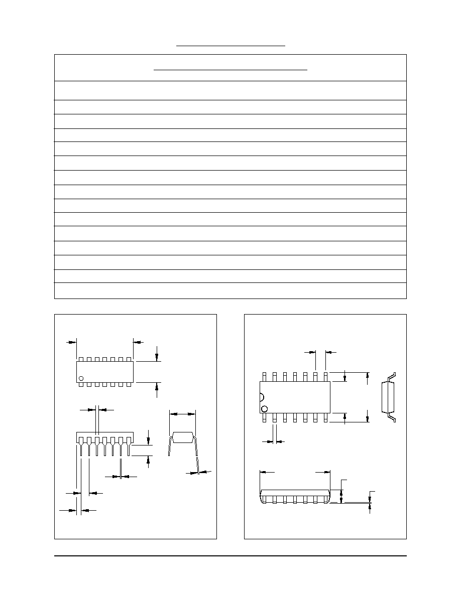
0.750±0.004
(19.05±0.10)
0.25±.004
(6.35±0.10)
0.32 Max.
(8.13)
0.060
(1.52)
0.075
(1.91)
0.10 Typ.
(2.54)
0.018
(0.46)
0.125±0.004
(3.18±0.10)
Typ.
1
0.010
(0.25)
Figure 2. Dual-In-Line Package Outline
0.050
(1.27)
Typ
0.245
(6.2)
Max
0.157
(3.99)
Max
0.018 (0.46)
Max
0.344 (8.74)
Max
0.069
(1.75)
Max
0.010
(0.25)
Max
1
Figure 3. Surface Mount Package Outline
Page 3
THAT140 Transistor Array
THAT Corporation; 45 Sumner St., Milford, Massachusetts; 01757-1656; USA
Tel: +1 (508) 478-9200; Fax: +1 (508) 478-0990; Web: www.thatcorp.com
Electrical Characteristics
2
Parameter
Symbol
Conditions
Min
Typ
Max
Units
NPN Current Gain
h
fe
V
CB
= 10 V
I
C
= 1 mA
60
100
æ
I
C
= 10 mA
60
100
æ
NPN Current Gain Matching
Dh
fe
V
CB
= 10 V, I
C
= 1 mA
--
5
--
%
NPN Noise Voltage Density
e
N
V
CB
= 10 V, I
C
= 1 mA, 1 kHz
--
0.8
--
nV / Hz
NPN Gain-Bandwidth Product
f
t
I
C
= 1 mA, V
CB
= 10 V
350
MHz
NPN DV
BE
(V
BE1
-V
BE2
)
V
OS
I
C
= 1 mA
--
±0.5
±3
mV
I
C
= 10 mA
--
±0.5
±3
mV
NPN DI
B
(I
B1
-I
B2
)
I
OS
I
C
= 1 mA
--
±500
±1500
nA
I
C
= 10 mA
--
±5
±15
nA
NPN Collector-Base
Leakage Current
I
CBO
V
CB
= 25 V
--
25
--
pA
NPN Bulk Resistance
r
BE
V
CB
= 0 V, 10mA < I
C
< 10mA
--
2
--
W
NPN Base Spreading Resistance
r
bb
V
CB
= 10 V, I
C
= 1mA
--
30
--
W
NPN Collector Saturation Voltage V
CE(SAT)
I
C
= 1 mA, I
B
= 100 mA
--
0.05
V
NPN Output Capacitance
C
OB
V
CB
= 10 V, I
E
= 0 mA, 100 kHz
3
pF
NPN Collector-Collector
Capacitance (Q
1
-Q
2
)
C
CC
V
CC
= 0 V, 100 kHz
0.7
pF
PNP Current Gain
h
fe
V
CB
= 10 V
I
C
= 1 mA
50
75
æ
I
C
= 10 mA
50
75
æ
PNP Current Gain Matching
Dh
fe
V
CB
= 10 V, I
C
= 1 mA
--
5
--
%
PNP Noise Voltage Density
e
N
V
CB
= 10 V, I
C
= 1 mA, 1 kHz
--
0.75
--
nV / Hz
PNP Gain-Bandwidth Product
f
t
I
C
= 1 mA, V
CB
= 10 V
325
MHz
PNP DV
BE
(V
BE3
-V
BE4
)
V
OS
I
C
= 1 mA
--
±0.5
±3
mV
I
C
= 10 mA
--
±0.5
±3
mV
PNP DI
B
(I
B3
-I
B4
)
I
OS
I
C
= 1 mA
--
±700
±1800
nA
I
C
= 10 mA
--
±7
±18
nA
PNP Collector-Base
Leakage Current
I
CBO
V
CB
= 25 V
--
-25
--
pA
PNP Bulk Resistance
r
BE
V
CB
= 0 V, 10mA < I
C
< 10mA
--
2
--
W
PNP Base Spreading Resistance
r
bb
V
CB
= 10 V, I
C
= 1mA
--
25
--
W
PNP Collector Saturation Voltage V
CE(SAT)
I
C
= 1 mA, I
B
= 100 mA
--
-0.05
V
PNP Output Capacitance
C
OB
V
CB
= 10 V, I
E
= 0 mA, 100 kHz
3
pF
PNP Collector-Collector
Capacitance (Q
3
-Q
4
)
C
CC
V
CC
= 0 V, 100 kHz
0.6
pF
1. All specifications subject to change without notice.
2. Unless otherwise noted, T
A
=25∞C.

THAT Corporation; 45 Sumner St., Milford, Massachusetts; 01757-1656; USA
Tel: +1 (508) 478-9200; Fax: +1 (508) 478-0990; Web: www.thatcorp.com
Rev. 11/29/00
Page 4
Notes