THAT Corporation; 45 Sumner Street; Milford, Massachusetts 01757-1656; USA
Tel: +1 508 478-9200; Fax: +1 508 478-0990; Web: www.thatcorp.com
THAT 1510, 1512
Description
The THAT 1510 and 1512 are high perfor-
mance audio preamplifiers suitable for micro-
phone preamp and bus summing applications.
The ICs are pin compatible with the Analog De-
vices SSM2017 in both the 8-pin DIP and
16-pin SOIC packages.
The THAT1512 follows a different gain
equation than the 1510, but exhibits signifi-
cantly lower noise at lower gain settings and is
recommended for new designs.
Designed from the ground up in THAT's
complementary
bipolar,
dielectric
isolation
process, the THAT 1510 and 1512 improve on
existing integrated microphone preamps by of-
fering lower noise at low gains, better distor-
tion characteristics, lower power consumption,
higher slew rate and bandwidth, and increased
output voltage swing. The parts are fully pro-
tected against ESD on all critical pins, and reli-
ability is further enhanced by their reduced
power requirements.
In short, the THAT 1510 and 1512 provide
superior performance in a popular format at an
affordable price.
T H A T
C o r p o r a t i o n
Low Noise, High Performance
Microphone Preamplifier IC
FEATURES
�
Excellent noise performance
through the entire gain range
�
Exceptionally low THD+N over the
full audio bandwidth
�
Low power consumption: 7mA typ.
�
Wide bandwidth: 3MHz typ. @
G=1000 (THAT 1510)
�
High Slew Rate: 28 V/
ms @ G=10
and C
L
=50pF (THAT 1510)
�
Wide Output Swing: �13V typ. on
�15V supplies
�
Gain adjustable from 1 to >1000
with a single external resistor
�
Drop-in compatible with SSM-2017
(THAT 1510)
APPLICATIONS
�
Mixing Consoles
�
Public Address Systems
�
Analog and Digital Snakes
�
Breakout Boxes for
Digital Systems
�
Sonar
�
Paging and Intercom systems
�
Instrumentation
V+
V-
-In
RG2
RG1
+In
Out
Ref
+
-
5k
5k
(10k)
5k
5k
(10k)
5k
5k
+1
+1
Figure 1. THAT 1510 / 1512 Equivalent Circuit Diagram
(THAT 1512 values shown in parentheses)
Pin Name
DIP
SO16
RG1
1
2
-In
2
4
+In
3
5
V-
4
7
Ref
5
10
Out
6
11
V+
7
13
RG2
8
15
Table 1. 1510 / 1512 pin assignments
Gain Equation
DIP-8
SO16
G
k
RG
= +
1
10
W
1510P
1510S
G
k
RG
=
+
0 5
5
.
W
1512P
1512S
Table 2. Ordering Information

THAT Corporation; 45 Sumner Street; Milford, Massachusetts 01757-1656; USA
Tel: +1 508 478-9200; Fax: +1 508 478-0990; Web: www.thatcorp.com
Page 2
THAT 1510 / 1512 Microphone Preamplifier
Preliminary Information
Absolute Maximum Ratings (T
A
= 25�C)
Positive Supply Voltage (V
CC
)
+20 V
Operating Temperature Range (T
OP
)
-40 to +85�C
Negative Supply Voltage (V
EE
)
-20 V
Storage Temperature Range (T
ST
)
-40 to +125�C
Output Short-Circuit Duration (t
SH
)
Continuous
Junction Temperature (T
J
)
150�C
Lead Temp. (T
LEAD
) (Soldering 10 sec)
260
�C
Electrical Characteristics
2
1510
1512
Parameter
Symbol
Conditions
Min
Typ
Max
Min
Typ
Max
Units
Supply Current
I
CC
, |I
EE
|
No signal
--
6.1
8.2
--
6.1
8.2
mA
V
CC
= |V
EE
| = 20V
--
--
8.4
--
--
8.4
mA
Input Bias Current
I
B
No signal; Either input
--
8.6
25
--
8.6
25
mA
connected to GND
Input Offset Current
I
B-OFF
No signal
--
--
�2.5
--
--
�2.5
mA
Output Referred Offset Voltage
Vos
OR
No Signal, V
CM
=0
--
--
� 50
--
--
� 25
mV
Input Referred Offset Voltage
Vos
IR
60 dB gain
--
--
� 1.2
--
--
� 1.2
mV
Input Voltage Range
Common Mode
V
IN-CM
Common mode, all gains
--
� 13
--
--
� 13
--
V
Normal Mode
V
IN-UNBAL
Unbalanced
--
� 13
--
--
� 13
--
V
One input to GND, 0dB gain
Differential Gain
G
diff
0
--
70
0
--
60
dB
Ref Input Voltage Range
--
� 8
--
--
� 8
--
V
Ref Input Impedance
--
10
--
--
15
--
k
W
Ref Input Gain to Output
--
0
--
--
0
--
dB
Input Impedance
Z
IN-DIFF
Differential
0dB gain
--
32||1.9
--
--
37||1.9
--
M
W||pF
20dB gain
--
32||2.0
--
--
37||2.0
--
M
W||pF
40dB gain
--
32||2.5
--
--
36||3.1
--
M
W||pF
60dB gain
--
29||8.0
--
-- 31||13.9 --
M
W||pF
Z
IN-CM
Common mode
all gains
--
8||7.7
--
--
9||7.7
--
M
W||pF
Recommended Operating Conditions
Parameter
Symbol
Conditions
Min
Typ
Max
Units
Positive Supply Voltage
V
CC
+5
+20
V
Negative Supply Voltage
V
EE
-5
-20
V
SPECIFICATIONS
1
1. All specifications are subject to change without notice.
2. Unless otherwise noted, V
CC
= +15V, V
EE
= -15V, T
A
=25�C,

THAT Corporation; 45 Sumner Street; Milford, Massachusetts 01757-1656; USA
Tel: +1 508 478-9200; Fax: +1 508 478-0990; Web: www.thatcorp.com
600031 Rev. 7/23/02
Page 3
Preliminary Information
Electrical Characteristics (Cont'd)
1510
1512
Parameter
Symbol
Conditions
Min
Typ
Max
Min
Typ
Max
Units
Common Mode Rejection
CMR
V
CM
=� 10V; DC to 60 Hz
0 dB gain
20
55
--
20
55
--
dB
20 dB gain
40
75
--
40
75
--
dB
40 dB gain
60
95
--
60
95
--
dB
60 dB gain
80
115
--
80
115
--
dB
Power Supply Rejection
PSR
V
CC
= |V
EE
|; �5V to �20V; DC to 60 Hz
0 dB gain
--
85
--
--
85
--
dB
20 dB gain
--
105
--
--
105
--
dB
40 dB gain
--
120
--
--
120
--
dB
60 dB gain
--
124
--
--
124
--
dB
Total Harmonic Distortion
THD+N
V
OUT
= 7Vrms; R
L
= 5 k
W
f = 1kHz; BW = 20 kHz
0 dB gain
--
0.0005
--
--
0.0005
--
%
20 dB gain
--
0.0005
--
--
0.0005
--
%
40 dB gain
--
0.0005
--
--
0.0005
--
%
60 dB gain
--
0.005
--
--
0.005
--
%
f = 20kHz; BW = 80 kHz
0 dB gain
--
0.002
--
--
0.002
--
%
60 dB gain
--
0.005
--
--
0.005
--
%
Equivalent Input Noise
e
n(OUT)
f = 1kHz,
0dB gain
--
57
--
--
34
--
nV/
�Hz
20dB gain
--
7
--
--
4.6
--
nV/
�Hz
40dB gain
--
1.7
--
--
1.4
--
nV/
�Hz
60dB gain
--
1
--
--
1
nV/
�Hz
Input Current Noise
i
n
60dB gain
--
2.3
--
--
2.3
--
pA/
�Hz
Noise Figure
NF
60dB gain
R
S
= 150
W
--
1.6
--
--
1.6
--
dB
R
S
= 200
W
--
1.3
--
--
1.3
--
dB
Slew Rate
SR
R
L
= 2 k
W
C
L
= 50 pF
16
28
--
16
24
--
V/
ms
Bandwidth -3dB
BW
-3dB
R
L
= 2 k
W; C
L
= 10 pF
0dB gain
--
15
--
--
11
--
MHz
20dB gain
--
8
--
--
9
--
MHz
40dB gain
--
7
--
--
7
--
MHz
60dB gain
--
3
--
--
1.6
MHz
Output Gain Error
G
ER (OUT)
f = 1kHz; R
L
= 2 k
W
0dB gain
--
� 0.25
� 1
--
� 0.25
� 1
dB
20dB gain
--
� 0.20
� 1
--
� 0.20
� 1
dB
40dB gain
--
� 0.20
� 1
--
� 0.20
� 1
dB
60dB gain
--
� 0.05 � 0.5
--
� 0.05 � 0.5
dB
Output Voltage Swing
V
O
R
L
= 2 k
W
all gains
�13
�13.3
--
�13
�13.3
--
V
Output Short Circuit Current
I
SC
R
L
= 0
W
--
�17
--
--
� 17
--
mA
Minimum Resistive Load
R
Lmin
--
2
--
--
2
--
k
W
Maximum Capacitive Load
C
Lmax
--
--
200
--
--
200
pF
Gain Equation
G
k
RG
= +
1
10
W
G
.
k
RG
=
+
0 5
5
W
Gain Resistor (ideal values)
RG
0dB gain
�
10k
W
20dB gain
1,100
526.3
W
40dB gain
101
50.3
W
60dB gain
10
5
W
Applications
Gain Setting
A single external resistor between the RG1 and
RG2 pins is all that is needed to set the gain of the
THAT 1510 / 1512, according to the formulae
for the 1510:
G
k
RG
= +
1
10
W
or
RG
k
G
=
-
10
1
W
for the 1512:
G
k
RG
=
+
0 5
5
.
W
or
RG
k
G
=
-
5
0 5
W
.
For unity gain operation on the 1510, RG1 and
RG2 may be left open. RG should be set to 10k
W in
the 1512. To avoid excess noise and ensure tempera-
ture stability, non-inductive wirewound or metal-film
resistors are recommended for RG.
Total gain accuracy will depend on both the toler-
ance on RG, and on the gain equation accuracy of the
THAT 1510/1512.
Total gain drift will result from
the mismatch between the tempco of RG and the
THAT Corporation; 45 Sumner Street; Milford, Massachusetts 01757-1656; USA
Tel: +1 508 478-9200; Fax: +1 508 478-0990; Web: www.thatcorp.com
Page 4
THAT 1510 / 1512 Microphone Preamplifier
Preliminary Information
RG
+In
3
4
Out
6
7
5
-In
2
RG1
1
RG2
8
U1
THAT
1510/1512
-15
+15
-In
+In
R1
1k
R2
1k
C1
470p
C2
470p
C3
47p
Out
C6
100n
C9
100n
V+
V-
Ref
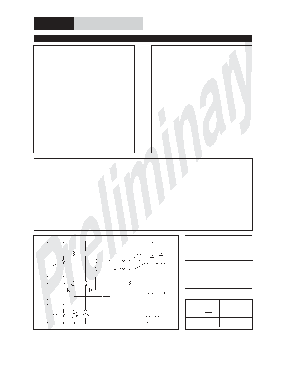
Figure 2. Basic 1510 / 1512 Circuit
RG
+In
3
4
Out
6
7
5
-In
2
RG1
1
RG2
8
U1
THAT 1510/1512
-In
+In
R1
1k
R2
1k
C1
470p
C2
470p
C3
47p
Out
3
2
6
U2
353
C8
100n
R3
510k
-15
+15
C6
100n
C9
100n
V+
V-
Ref
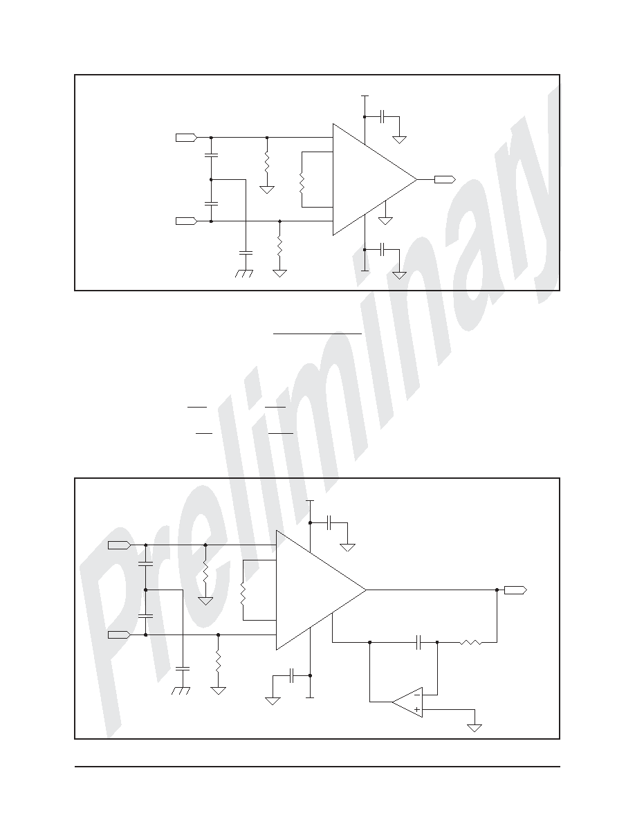
Figure 3. 1510 / 1512 Circuit with Output Offset Correction
tempco of the internal resistors (�20 ppm/�C typi-
cal).
Noise Performance
Thoughtful design results in these devices having
significantly lower noise at low gains than similar IC
microphone preamps. At zero dB gain, equivalent in-
put noise of the THAT 1510 is 55 nV/
�Hz, nearly
6 dB better than competitive IC designs.
The un-
usual topology of the THAT 1512 results in an equiv-
alent input noise of 34 nV/
�Hz at zero dB gain, which
makes it comparable to some of the better discrete
designs currently available.
At 1 kHz, the equivalent
input noise for both devices is 1 nV/
�Hz at 60 dB
gain.
Inputs
Protection diodes are employed at all pins except
V+ and V- of the THAT 1510/1512. These diodes re-
duce the likelihood of accidental ESD/EOS damage to
the IC. Other diodes across the base-emitter junc-
tions of the input transistors prevent reverse bias of
these junctions and consequent degradation of their
noise performance.
The inputs of the THAT 1510 and1512's are float-
ing, so a dc bias connection is required to maintain
the inputs within the IC's input common-mode range.
Four different schemes are shown in Figures 2, 3, 4,
and 5. Note that the values of R1 and R2 in these fig-
ures should be kept small to minimize pickup of un-
wanted noise and interference.
A value of 1 k
W is
often used, since some microphones require a differ-
ential input impedance of this magnitude. Unfortu-
nately, one would usually desire a significantly higher
common mode input impedance to minimize the
common mode degradation caused by unbalanced
source impedances.
Figure 5 shows a technique
which allows higher common mode input impedance
while maintaining a lower differential source imped-
ance.
Reference Terminal
The "Ref" pin provides the reference for the out-
put signal, and is normally connected to analog
ground. If necessary, the "Ref" pin can be used for
offset correction or DC level shifting. A non-zero ref-
erence source resistance will reduce the IC's com-
mon-mode
rejection
(CMR)
by
the
ratio
of
10 k
W/R
REF
.
Phantom Power
Phantom power is required for condensor micro-
phones. A phantom power circuit is shown in Fig-
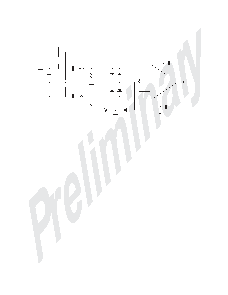
ure 4.
Diodes D1 through D6 are necessary to
protect the THAT 1510/1512 from transient voltages
THAT Corporation; 45 Sumner Street; Milford, Massachusetts 01757-1656; USA
Tel: +1 508 478-9200; Fax: +1 508 478-0990; Web: www.thatcorp.com
600031 Rev. 7/23/02
Page 5
Preliminary Information
RG
+In
3
4
Out
6
7
5
-In
2
RG1
1
RG2
8
U1
THAT 1510
In-
In+
R1
1k
R2
1k
C1
470p
C2
470p
C3
47p
Out
C4
47u
C5
47u
D1
1N757
D2
1N757
R3
51R
R4
51R
R6
6k8
R5
6k8
+48V
D3
1N5818
D4
1N5818
D5
1N5818
D6
1N5818
-15
+15
C6
100n
C9
100n
Ref
V-
V+
Figure 4. Typical 1510 / 1512 Circuit with Phantom Power