 | –≠–Ľ–Ķ–ļ—ā—Ä–ĺ–Ĺ–Ĺ—č–Ļ –ļ–ĺ–ľ–Ņ–ĺ–Ĺ–Ķ–Ĺ—ā: THAT 1606 | –°–ļ–į—á–į—ā—Ć:  PDF PDF  ZIP ZIP |

THAT Corporation; 45 Sumner Street; Milford, Massachusetts 01757-1656; USA
Tel: +1 (508) 478-9200; Fax: +1 (508) 478-0990; Web: www.thatcorp.com
THAT
1606, 1646
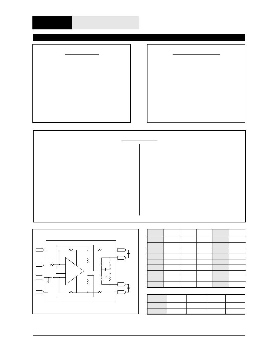
Description
The THAT 1606 and 1646 are a new generation
of monolithic audio differential line drivers offering
improved performance over conventional cross-cou-
pled designs. Based on a high-performance, fully dif-
ferential
opamp
and
laser-trimmed
thin-film
resistors, both families exhibit low noise and distor-
tion, high slew rate, and wide output swing.
The
parts are stable when driving difficult loads, and
have short-circuit protected outputs.
Designed from the ground up in THAT's comple-
mentary dielectric isolation process, both models in-
corporate THAT's patented OutSmarts
1
technology.
This is a dual feedback-loop design that prevents the
excessive ground currents typical of cross-coupled
output
stages
(CCOS)
when
clipping
into
sin-
gle-ended loads. OutSmarts uses two individual neg-
ative-feedback
loops
to
separately
control
the
differential output voltage and common mode output
currents, making the designs inherently more stable
and less sensitive to component tolerances than
common CCOSes. As a result, THAT's topology pre-
vents the loss of common-mode feedback that
plagues common CCOS designs when clipping into
single-ended loads. This avoids excessive ground
currents that would otherwise upset power supplies
and create additional distortion, even in adjacent
channels.
The 1646 is pin-compatible with the TI DRV134
and
DRV135,
as
well
as
the
Analog
Devices
SSM2142. The 1606 offers an advanced com-
mon-mode offset voltage reduction scheme, which re-
quires a small single capacitor instead of the two
electrolytics
required
by
the
1646
and
its
pin-compatible cousins. Additionally, the 1606 fea-
tures differential inputs in a space-saving 16-pin
QSOP package. Both parts offer +6 dB gain.
T H A T
C o r p o r a t i o n
OutSmarts
TM
Balanced Line Driver ICs
FEATURES
∑
Balanced, transformer-like floating
output
∑
OutSmarts technology improves
clipping into single-ended loads
∑
Stable driving long cables and
capacitive loads
∑
High output: 18Vrms into 600
∑
Low noise: -101 dBu
∑
Low distortion: 0.0007% @ 1kHz
∑
Industry-standard pinout
APPLICATIONS
∑
Differential Line Drivers
∑
Audio Mixing Consoles
∑
Distribution Amplifiers
∑
Hi-Fi Equipment
∑
Audio Equalizers
∑
Dynamic Range Processors
∑
Digital Effects Processors
∑
Telecommunications Systems
∑
Instrumentation
Din+
Cin+
Cin-
Din-
Out-
Sns+
Out+
Sns-
Vcc
In+
Vee
Gnd
Dout-
Dout+
10k
10k
25
5k
5k
10k
10k
10k
10k
20k
20k
10p
25
THAT 1646
C
EXT
C
EXT
D
C
A
A
&
Figure 1. THAT 1646 Equivalent Circuit Diagram
1646
Pin
SO8
Pin no.
DIP8
Pin no.
SO16W
Pin no.
1606
Pin
QSOP16
Pin no.
Out-
1
1
3
Out-
3
Sns-
2
2
4
Cap1
4
Gnd
3
3
5
Gnd
5
In
4
4
6
In-
6
Vee
5
5
11
In+
7
Vcc
6
6
12
Vee
11
Sns+
7
7
13
Vcc
12
Out+
8
8
14
Cap2
13
Out+
14
Table 1. THAT 1600 Series pin assignments
Model
SO8
Pkg
DIP8
Pkg
SO16W
Pkg
QSOP16
Pkg
1646
1646S08-U
1646P08-U
1646W16-U
---
1606
---
---
---
1606Q16-U
Table 2. Order Number Information
1. For complete details of OutSmarts, see Hebert, Gary K., "An Improved Balanced, Floating Output Driver IC", presented at the 108th AES Convention, February 2000.
Protected under US Patents numbers 4,979,218 and 6,316,970. Additional patents pending. THAT is a registered trademark of THAT Corporation; OutSmarts is a
trademark of THAT Corporation.
600078 Rev 00

THAT Corporation; 45 Sumner Street; Milford, Massachusetts 01757-1656; USA
Tel: +1 (508) 478-9200; Fax: +1 (508) 478-0990; Web: www.thatcorp.com
Page 2
THAT1606/1646 Balanced Line Driver
Absolute Maximum Ratings (T
A
= 25įC)
Positive Supply Voltage (Vcc)
+20 V
Storage Temperature (T
ST
)
-55 to +125
į
C
Negative Supply Voltage (Vee)
-20 V
Junction Temperature (T
J
)
125
į
C
Output Short Circuit Duration
Continuous
Lead Temperature (T
LEAD
)(Soldering 60 sec)
300
į
C
Operating Temperature Range (T
OP
)
-40 to +85
į
C
SPECIFICATIONS
2
2. All specifications are subject to change without notice.
3. Unless otherwise noted,.all measurements taken with V
S
=Ī18V, T=25
į
C, R
L
= 600
W
Balanced, R
SOURCE
= 0
W
1646 Electrical Characteristics
3
Parameter
Symbol
Conditions
Min.
Typ.
Max.
Units
Input Impedance
Z
IN
4.00
5.00
k
Gain
G1
R
L
=100 k
per output
Balanced
5.80
6.00
6.20
dB
Single Ended
5.76
5.96
6.16
dB
Gain
G2
R
L
= 600
Balanced
5.00
5.30
5.60
dB
Single Ended
4.96
5.26
5.56
dB
Gain Error
G1
R
L
=100 k
per output, Balanced
0.02
0.20
dB
DC Power Supply
Rejection Ratio
PSRR
Ī4V to Ī18V
85
107
dB
Output Common-Mode
Rejection Ratio
OCMRR
f=1kHz, BBC Method
46
65
dB
Output Signal Balance Ratio
SBR
f=1kHz, BBC Method
35
54
dB
THD+N (Balanced)
THD+N
1
V
O
=10 V
RMS
, R
L
=600
20Hz-5kHz
0.0007
%
20kHz
0.002
0.005
%
THD+N (Single Ended)
THD+N
2
V
O
=10 V
RMS
, R
L
=600
20Hz-5kHz
0.0010
%
20kHz
0.0030
0.0060
%
Output Noise
Onoise
Balanced, 22Hz -20kHz
-101
dBu
Maximum Output Level
Vo
MAX
0.1% THD+N
27.5
dBu
Slew Rate
SR
C
L
=50pF/output
15
V/
Ķ
S
Small Signal Bandwidth
C
L
=50pF/output
10
MHz
Output Common Mode
Voltage Offset
V
OCM1
w/o Sense capacitors
-250
Ī50
250
mV
V
OCM2
w/ Sense capacitors
-15
Ī3.5
15
mV
Differential Output Offset
V
OD
-15
Ī4
15
mV
Output Voltage Swing, Positive
No Load
V
CC
≠2.9 V
CC
≠2.2
V
Output Voltage Swing, Negative
No Load
V
EE
+2.25 V
EE
+2.9
V
Output Impedance
Z
O
40
50
60

THAT Corporation; 45 Sumner Street; Milford, Massachusetts 01757-1656; USA
Tel: +1 (508) 478-9200; Fax: +1 (508) 478-0990; Web: www.thatcorp.com
Document 600078 Rev 00
Page 3
Maximum Capacitive Load
Stable Operation
Unlimited
ĶF
Quiescent Supply Current
I
S
Unloaded
4.5
5.5
mA
Output Short Circuit Current
I
SC
Both outputs to ground
70
mA
Power Supply Voltage Range
Ī4
Ī18
V
1646 Electrical Characteristics (cont'd)
Parameter
Symbol
Conditions
Min.
Typ.
Max.
Units
1606 Electrical Characteristics
3
Parameter
Symbol
Conditions
Min.
Typ.
Max.
Units
Input Impedance
Z
IN
4.00
5.00
k
Gain
G1
R
L
=100 k
/ output
Balanced
5.80
6.00
6.20
dB
Single Ended
5.76
5.96
6.16
dB
Gain
G2
R
L
= 600
Balanced
5.00
5.30
5.60
dB
Single Ended
4.96
5.26
5.56
dB
Gain Error
G1
R
L
=100 k
/ output, Balanced
0.02
0.20
dB
DC Power Supply
Rejection Ratio
PSRR
Ī4V to Ī18V
85
107
dB
Output Common-Mode
Rejection Ratio
OCMRR
f=1kHz, BBC Method
46
65
dB
Input Common-Mode
Rejection Ratio
ICMRR
f=1kHz
40
60
dB
Output Signal Balance Ratio
SBR
f=1kHz, BBC Method
35
54
dB
THD+N (Balanced)
THD+N
1
V
O
=10 V
RMS
, R
L
=600
20Hz-5kHz
0.0007
%
20kHz
0.002
0.005
%
THD+N (Single Ended)
THD+N
2
V
O
=10 V
RMS
, R
L
=600
20Hz-5kHz
0.0010
%
20kHz
0.0030
0.0060
%
Output Noise
Onoise
Balanced, 22Hz -20kHz
-101
dBu
Maximum Output Level
Vo
MAX
0.1% THD+N
27.5
dBu
Slew Rate
SR
C
L
=50pF/output
15
V/
Ķ
S
Small Signal Bandwidth
C
L
=50pF/output
10
MHz
Common Mode Output
Voltage Offset
V
OCM1
w/o CM coupling capacitor
-250
Ī50
250
mV
V
OCM2
w/ CM coupling capacitor
-20
-5
20
mV
Differential Output Offset
V
OD
-15
Ī4
15
mV
Output Voltage Swing, Positive
No Load
V
CC
≠2.9 V
CC
≠2.2
V
Output Voltage Swing, Negative
No Load
V
EE
+2.25 V
EE
+2.9
V
Output Impedance
Z
O
40
50
60
Maximum Capacitive Load
Stable Operation
Unlimited
ĶF
Quiescent Supply Current
I
S
Unloaded
4.5
5.5
mA

THAT Corporation; 45 Sumner Street; Milford, Massachusetts 01757-1656; USA
Tel: +1 (508) 478-9200; Fax: +1 (508) 478-0990; Web: www.thatcorp.com
Page 4
THAT1606/1646 Balanced Line Driver
Out-
Cap1
Cap2
Out+
Vcc
In+
Vee
In-
10k
10k
25
5k
5k
10k
10k
10k
10k
7k
7k
10p
25
THAT 1606
C
EXT
R
EXT
Din+
Cin+
Cin-
Din-
Dout-
Dout+
Gnd
D
C
A
A
&
Figure 3. THAT 1606 Equivalent Circuit Diagram
Din+
Cin+
Cin-
Din-
Out-
Sns+
Out+
Sns-
Vcc
In+
Vee
Gnd
Dout-
Dout+
10k
10k
25
5k
5k
10k
10k
10k
10k
20k
20k
10p
25
THAT 1646
C
EXT
C
EXT
D
C
A
A
&
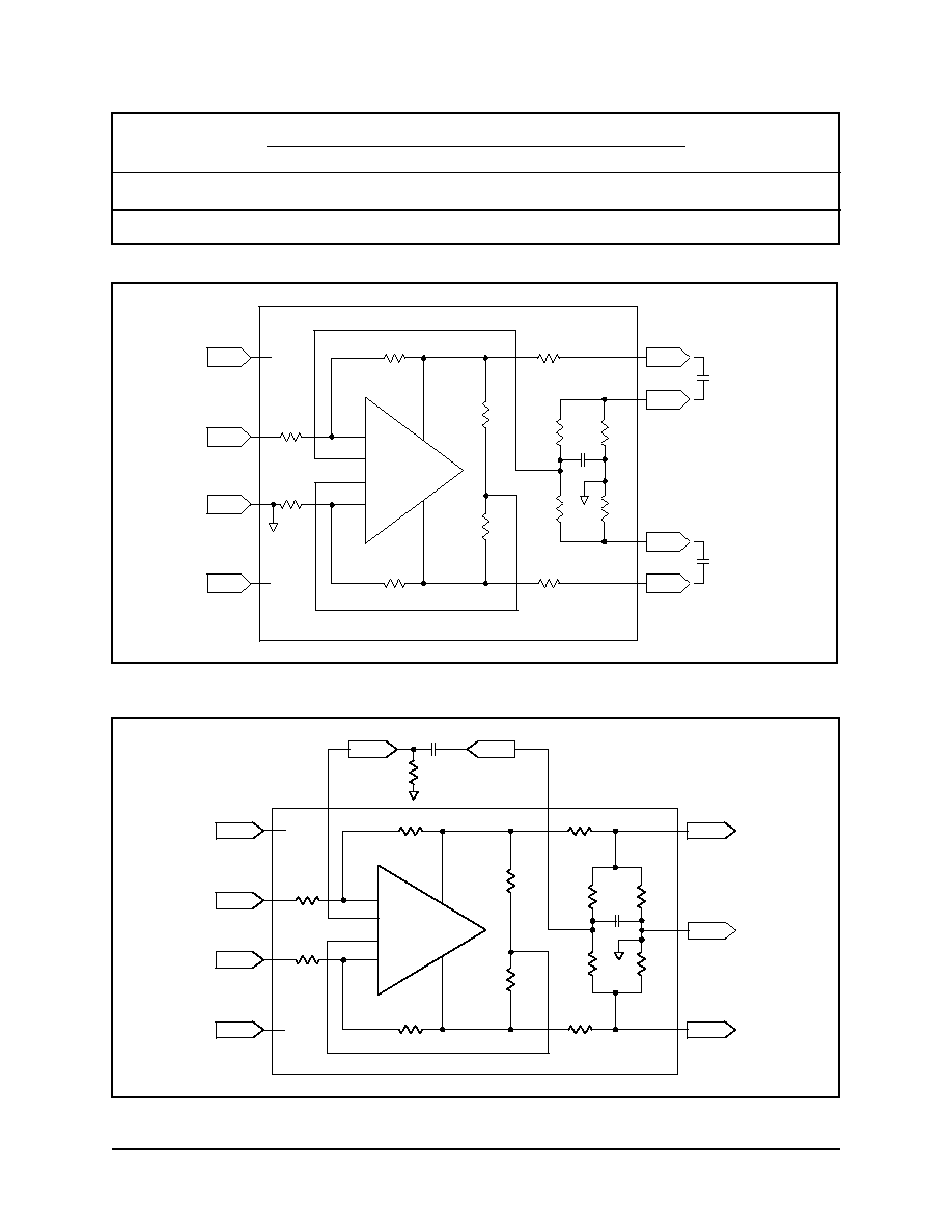
Figure 2. THAT 1646 Equivalent Circuit Diagram
Output Short Circuit Current
I
SC
Both outputs to ground
70
mA
Power Supply Voltage Range
Ī4
Ī18
V
1606 Electrical Characteristics (cont'd)
Parameter
Symbol
Conditions
Min.
Typ.
Max.
Units

Theory of Operation
OutSmarts
TM
technology
The THAT 1606 and 1646 family employs the
OutSmarts topology, a variation of circuitry originally
developed by Chris Strahm at Audio Teknology Inc.,
(and later acquired by Audio Toys, Inc.).
THAT's
OutSmarts topology employs two negative-feedback
loops -- one to control the differential signal, and a
separate loop to control the common mode output
levels.
Figures 2 and 3 show the gain core common to
the 1606 and 1646. The gain core is a single ampli-
fier that includes two differential input pairs, Cin+/-
and Din+/-, and complementary outputs, Vout+ and
Vout-, related to each other by two gain expressions,
A
D
(s) and A
C
(s). The first pair of differential inputs,
Din+/-, is connected to the differential feedback net-
work between the outputs and the input signal. The
second differential input pair, Cin+/-, is connected to
a bridge circuit which generates an error signal used
to servo the common-mode behavior of the outputs.
The loop equations are then:
(
)
D
D
D
A
D
D
OUT
OUT
OUT
D
IN
IN
+
-
+
-
-
=
=
-
,
where AD is the differential open-loop gain, and
(
)
D
D
D
A
C
C
OUT
OUT
OUT
C
IN
IN
+
-
+
-
+
=
=
-
,
where AC is the common-mode open-loop gain.
These equations can be solved much like stan-
dard op-amp loop equations.
For the differential case, using superposition, we
can see that this results in:
D
D
In
IN
OUT
+
-
+
=
+
1
3
2
3
, and
D
D
In
IN
OUT
-
+
=
+
-
1
3
2
3
.
Substituting and simplifying into the equation
that defines differential operation yields:
[
]
D
A
In
In
OUT
D
D
OUT
=
+
-
-
+
-
3
2
3
(
) .
Dividing through by A
D
(assuming that A
D
>> 3) and
simplifying yields
(
)
D
In
In
OUT
=
-
+
-
2
.
as one would expect for a +6 dB line driver.
For the 1646, In- is hard-wired to ground (0v), so
the differential equation above simplifies to:
( )
D
In
OUT
=
+
2
.
The common mode equation is more complicated
in that it is dependent on the attached load, and in
any event doesn't yield much insight into the device's
operation.
For those who are interested, a more
complete discussion is given in the reference men-
tioned in note 1.
In op-amp analysis using negative feedback loops,
the combination of negative feedback and high
open-loop gain usually results in the open-loop gain
"dropping out" of the equation, and the differential in-
puts being forced to the same potential. This is true
for the core of the 1606 and 1646 ICs. If we start
with that assumption, the operation of the com-
mon-mode feedback loop can be intuited as follows:
Referring again to Figures 2 and 3, the common-
mode input actually senses the sum of each IC's out-
put currents by way of two 25 resistors and the
bridge network
4
. The resulting error signal is ampli-
fied and then summed into both outputs, with the net
effect being to force the sum of the currents to be
zero, and thus the common mode output current to
zero.
To see why this is important, consider what hap-
pens when the IC is loaded with a single-ended load,
which shorts one or the other output to ground.
Suppose Out- is grounded. In this case, the differen-
tial feedback loop increases the voltage at Dout+ to
make up for most of the signal lost to the short at
Out-.
The common-mode feedback loop forces the
current from Out- to be equal and opposite to that
from Out+. But, during peak signals which drive
Dout+ into clipping (exceeding its maximum output
voltage capability), the differential loop is starved for
feedback. Without the common-mode feedback, the
result would be for the voltage at Dout- to decrease in
an attempt to satisfy the differential loop's demand
for feedback.
This is one significant weakness of
conventional cross-coupled output designs ≠ com-
mon-mode feedback is lost when one output is
clipped while the other is grounded.
With OutSmarts, however, the common mode
feedback loop senses this happening because of the
increase in current at Out- (compared to that at
Out+), and prevents the voltage at Out- from rising
THAT Corporation; 45 Sumner Street; Milford, Massachusetts 01757-1656; USA
Tel: +1 (508) 478-9200; Fax: +1 (508) 478-0990; Web: www.thatcorp.com
Document 600078 Rev 00
Page 5
4. The 10 pf capacitor can be ignored for the purposes of this analysis. It simply limits the maximum frequency at which the current-sensing action occurs

out of control. This causes the OutSmarts design to
more closely mimic the behavior of a true floating
balanced source (such as a transformer), compared
to the behavior of a conventional CCOS design.
Applications
Circuit implementations using the 1606 and 1646
are relatively straightforward. A quiet, solid ground
reference, stiff voltage supplies, and adequate supply
bypassing are all that are required to achieve excel-
lent performance out of both ICs. Both devices must
be driven from a low-impedance source, preferably
directly from opamp outputs, to maintain the
specified performance.
Stability and Load Capacitance
The devices are stable into any capacitive load,
and the maximum capacitance is limited only by slew
rate and frequency response considerations.
For the purposes of the frequency response calcu-
lation, the line driver's 25 sense resistors can be
lumped into a single 50 resistor. The correct cable
capacitance to use for the balanced-signal case is the
sum of the inter-conductor capacitance and the two
conductor-to-shield capacitances in series.
Some
manufacturers only specify the inter-conductor ca-
pacitance and the capacitance of one conductor to
the other while connected to the shield, and some ex-
traction may be required.
As an example, Belden 8451 is specified as hav-
ing with 34 pF/ft of inter-conductor capacitance and
67 pF/ft of conductor to "other conductor + shield
capacitance". Thus, we can assume a single conduc-
tor-to-shield capacitance of 33 pF/ft (the difference
between 67 and 34) for each conductor. For balanced
signals, the load capacitance across the 1646 outputs
will be 34 pF/ft + 16.5 pF/ft = 50.5 pF/ft. The corner
frequency of the THAT 1646 driving 500 ft of this ca-
ble (25.25 nF) will be 126 kHz.
f
kHz
C
pF
ft
pF
ft
=
=
◊ ◊
◊
+
1
2
50
500 34
16 5
126
(
.
)
One must also consider the slew rate limitations
posed by excessive cable and other capacitances. We
know that
i
C
dV
dt
=
and that
dV
dt
Peak
V
f
=
◊ ◊
2
Dennis Bohn of Rane Corporation has published
work specifying some of the requirements for a bal-
anced line driver, including a) stability into reactive
loads, b) differential output voltage swing of at least
Ī11 volts peak (+20dBu), and c) reliability
5
. This
work suggests a reasonable rule by which to calculate
the output current requirements at 20kHz. The au-
thor concludes that the actual worst case peak level
THAT Corporation; 45 Sumner Street; Milford, Massachusetts 01757-1656; USA
Tel: +1 (508) 478-9200; Fax: +1 (508) 478-0990; Web: www.thatcorp.com
Page 6
THAT1606/1646 Balanced Line Driver
In
4
Gnd
3
5
2
Out-
1
Out+
8
7
6
U1
THAT1646
In
Vcc
Vee
2
3
C4
100n
C5
100n
Vcc
Sns+
Vee
Sns-
1
XLR (M)
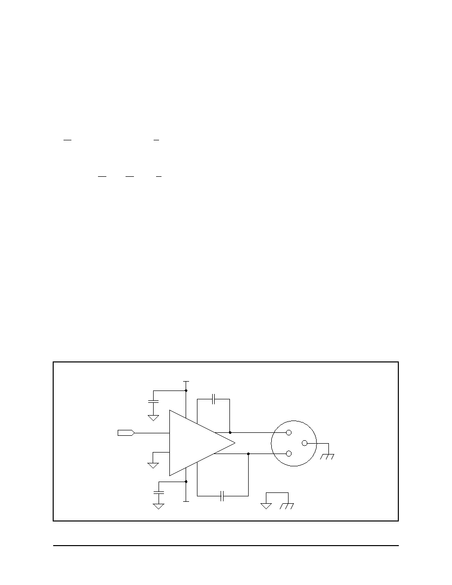
Figure 4. Basic THAT 1646 application circuit
5. Dennis A. Bohn, "Practical Line-Driving Current Requirements"(Rane Note 126), Rane Corporation, 1991, revised 5/1996. Available at www.rane.com/note126.html.

for various types of music and speech will be flat out
to 5kHz, and roll off at 6dB/octave above this fre-
quency. Thus the peak levels at 20kHz will be 12dB
below those at 5kHz.
Using these, we can calculate the required slew
rate and current drive. For the +26 dBu output lev-
els that the 1646 is capable of, VPeak is 22V (below
5kHz), and at 20kHz, VPeak is 5.5V. Therefore,
dV
dt
V
s
V
kHz
=
◊
◊
=
2
5 5
20
0 69
Ķ
.
.
As a consequence,
i
ft
mA
pF
ft
pF
ft
V
s
=
◊
+
◊
=
500
34
16 5
0 69
17 5
(
.
)
.
.
Ķ
.
Thus, driving this 25.25 nF cable requires 17.5
mA
Peak
, which is well within the capability of the
1606 and 1646.
Gain structure
The 1606 and 1646 both provide +6 dB gain (fac-
tor of 2) between their inputs and differential out-
puts.
This is appropriate, since with a balanced
output, twice the voltage between the power supply
rails is available at the output of the stage. The sin-
gle-ended input of the 1646 can accept signals that
swing to nearly the power supply rails without distor-
tion, when driving into a differential (floating) load.
The balanced input of the 1606 can accept signals at
each input that swing to nearly one-half the power
supply rails without distortion, when driving into dif-
ferential loads.
Both devices, when driving single-ended loads,
will clip at about half the output voltage as compared
to a differential load. This is because only one of the
two output signals will be available. Despite the out-
put clipping, the input to the devices does not need to
be constrained - they will work without undue prob-
lems being overdriven at their inputs when the out-
puts are clipping into single-ended loads.
1646 circuits
Figure 4 shows the most basic connection for a
1646. The only external components needed are the
local 100nF bypass capacitors.
These should be
within 1 inch of the 1646 pins.
Output DC offset
Because the 1646's outputs are connected directly
to their respective sense inputs, this circuit may pro-
duce up to 250mV of common-mode dc offset at its
outputs. As shown, the outputs are DC coupled to
the output connector, so this dc will appear directly
at the output of the system.
The output common-mode offset of a 1646 may
be reduced by adding capacitors in the feedback
loop, as shown in Figure 5. Capacitors C1 and C2
ac-couple the common-mode feedback loop.
This
changes the loop operation from servoing the com-
mon-mode output current at audio frequencies to
servoing the common-mode output voltage to 0 at
DC. This results in much lower common-mode out-
put offset voltage, as indicated in the specifications
section.
THAT Corporation; 45 Sumner Street; Milford, Massachusetts 01757-1656; USA
Tel: +1 (508) 478-9200; Fax: +1 (508) 478-0990; Web: www.thatcorp.com
Document 600078 Rev 00
Page 7
In
4
Gnd
3
5
2
Out-
1
Out+
8
7
6
U1
THAT1646
In
Vcc
Vee
2
3
C4
100n
C5
100n
Vcc
Sns+
Vee
Sns-
1
C1
10u
C2
10u
XLR (M)
Figure 5. THAT 1646 application circuit with common-mode offset reduction

1606 circuits
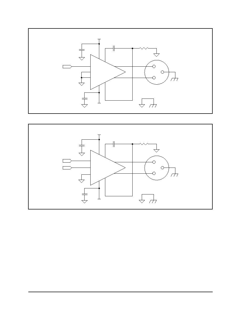
Figure 6 shows the most basic connection for a
1606.
The 1606 differs from the 1646 in two re-
spects. First, the 1606 includes a negative-sense in-
put pin (pin 6), so offers a differential input.
This
can be useful in connecting the output driver to the
output of modern D/A converters, which usually pres-
ent differential outputs. Second, instead of two 10uF
capacitors, the 1606 uses an 0.1uf capacitor (C1)
and 1M (R1) resistor to reduce common-mode dc
offset. Generally, these components will cost less, and
take up less space on the circuit board than the two
large capacitors required for the 1646. Because C1
is not in the differential signal path, it may be a ce-
ramic type without audible effect.
RFI protection
These line drivers can easily drive cables hun-
dreds of feet in length without becoming unstable,
but such long cables can act as antennae which can
pick up RFI and direct it into the circuit. The circuit
of Figure 8 includes two 100 pF bypass capacitors C3
and C8 and two ferrite beads, whose purpose is to
redirect this RF energy to the chassis before it can
circulate inside the product's box and couple RF into
THAT Corporation; 45 Sumner Street; Milford, Massachusetts 01757-1656; USA
Tel: +1 (508) 478-9200; Fax: +1 (508) 478-0990; Web: www.thatcorp.com
Page 8
THAT1606/1646 Balanced Line Driver
In+
7
Gnd
6
Out-
3
Out+
14
4
U1
THAT1606
In
Vcc
Vee
2
3
C4
100n
C5
100n
Vcc
Cap1
Vee
Cap2
1
C1
100n
12
13
11
In-
5
R1
1M0
XLR (M)
Figure 6. Basic THAT 1606 application circuit with output common mode offset reduction and single-ended input drive
In+
7
Gnd
6
Out-
3
Out+
14
4
U1
THAT1606
In+
Vcc
Vee
2
3
C4
100n
C5
100n
Vcc
Cap1
Vee
Cap2
1
C1
100n
12
13
11
In-
5
R1
1M0
In-
XLR (M)
Figure 7. Basic THAT 1606 application circuit with output common mode offset reduction and differential drive

other portions of the circuit. The capacitors should
be located as close as possible to the output connec-
tor and connected via a low-inductance path to chas-
sis ground, with the ferrite beads placed very nearby.
These components ensure that RFI current is di-
rected to the chassis and not through the relatively
low-impedance output of the 1646. The bypass ca-
pacitors and ferrite beads will have no effect on the
gain error of these line drivers at audio frequencies.
The same RF protection scheme applies to the
1606.
Output protection
The 1606 and 1646 each incorporate a propri-
etary internal protection scheme, which will suffice
for most situations seen in the field.
For instance,
one might foresee having the line driver's output mis-
takenly
plugged
directly
into
a
microphone
preamplifier input that has +48V phantom power ap-
plied. When this happens, the ac coupling capacitors
on the preamp's input will discharge into the
low-impedance output of the 1606/1646.
This can
result in surge currents of over 2 amperes
6
.
The
amount of energy stored in these capacitors is di-
THAT Corporation; 45 Sumner Street; Milford, Massachusetts 01757-1656; USA
Tel: +1 (508) 478-9200; Fax: +1 (508) 478-0990; Web: www.thatcorp.com
Document 600078 Rev 00
Page 9
In+
7
Gnd
6
In+
In-
5
In-
D3
1N4004
D4
1N4004
D5
1N4004
D6
1N4004
C3
100p
C8
100p
L1
Ferrite Bead
L2
Ferrite Bead
2
3
1
Out-
3
Out+
14
4
U1
THAT1606
Vcc
Vee
C4
100n
C5
100n
Vcc
Cap1
Vee
Cap2
C1
100n
12
13
11
R1
1M0
XLR (M)
Figure 9. 1606 with output common mode offset protection, RFI protection, and surge protection
In
4
Gnd
3
Out-
1
Out+
8
U1
THAT1646
In
Vcc
Vee
C1
10u
C2
10u
C4
100n
C5
100n
C3
100p
C8
100p
L1
Ferrite Bead
L2
Ferrite Bead
5
6
7
2
Vee
Sns-
Sns+
Vcc
2
3
1
XLR (M)
Figure 8. 1646 with output common mode offset protection and RFI protection
6. Hebert, Gary K., Thomas, Frank w., "The 48V Phantom Menace", presented at the 110th Audio Engineering Society Convention, May, 2001

rectly proportional to the capacitor value, which is, of
course, not under the 1606/1646 designer's control.
The 1606/1646's internal protection network will
withstand this abuse for coupling capacitors up to
about 33 uF.
To protect against microphone preamplifiers that
incorporate larger values of capacitance, a pair
1N4004 diodes from each output to the supply rails,
as shown in Figure 9, is recommended. This shunts
the discharge current to the power supply bypass
and filter capacitors, thus protecting the output of
the 1606 or 1646. Note that Figure 9 shows a 1606,
but a 1646, with appropriate connection as shown in
Figure 4 or Figure 5, may be substituted.
Closing thoughts
The integrated balanced line driver is one of those
highly useful, cost-effective functional blocks that can
provide significant improvement over discrete de-
signs. The THAT 1646 goes a step or two further by
improving over existing components. Both incorpo-
rate OutSmarts technology to tame the aberrant sin-
gle-ended
clipping
behavior
of
conventional
cross-coupled output stages.
For more information on these or other THAT
Corporation integrated circuits, please contact us di-
rectly, or through one of our international distribu-
tors.
Package Information
The THAT1646 in available in 8-pin SO, 8-pin
mini-DIP and 16-pin wide SOIC packages. The 1606
comes in a 16-pin QSOP package
Package dimen-
sions are shown in Figures 10, 11, 12 and 13, while
pinouts are given in Table 1.
Thermal Considerations
As mentioned. the 1646 is available in an 8-pin
DIP, and 16-pin wide SO, and an 8-pin SO, with junc-
tion-to-ambient thermal resistances of 100įC/watt,
80įC/watt, and 150įC/watt, respectively, assuming a
2-sided PCB with no ground planes.
Users of the
SO-8 package should recognize driving 600 loads
or very long cables (several hundred feet) at high am-
bient temperatures (above 55įC) continuously could
lead to internal die temperatures that exceed the
maximum rating and result in performance degrada-
tion.
The 1606 is supplied in a 16-pin QSOP package
in which pins 1, 8, 9, and 16 are fused to the die
paddle to assist in conducting heat away from the
die. These pins are connected to the die substrate,
which is, in turn, connected to the ground pin of the
device. When these pins are connected to a top-side
ground plane of 1 square inch area, the junc-
tion-to-ambient thermal resistance is 125įC/watt. In-
ternal planes on multi-layer PCBs will reduce the
thermal resistance further.
THAT Corporation; 45 Sumner Street; Milford, Massachusetts 01757-1656; USA
Tel: +1 (508) 478-9200; Fax: +1 (508) 478-0990; Web: www.thatcorp.com
Page 10
THAT1606/1646 Balanced Line Driver

THAT Corporation; 45 Sumner Street; Milford, Massachusetts 01757-1656; USA
Tel: +1 (508) 478-9200; Fax: +1 (508) 478-0990; Web: www.thatcorp.com
Document 600078 Rev 00
Page 11
A
D
1
B
C
E
I
J
0-8ļ
G
H
ITEM
MILLIMETERS
INCHES
A
4.80 - 4.98
0.189 - 0.196
B
3.81 - 3.99
0.150 - 0.157
C
5.79 - 6.20
0.228 - 0.244
D
0.20 - 0.30
0.008 - 0.012
E
0.635 BSC
0.025 BSC
G
1.35 - 1.75
0.0532 - 0.0688
H
0.10 - 0.25
0.004 - 0.010
I
0.40 - 1.27
0.016 - 0.050
J
0.19 - 0.25
0.0075 - 0.0098
Figure 13. 16 pin QSOP package outline drawing
D
E
B
C
J
A
F
H
G
1
ITEM
A
B
C
D
E
F
G
H
J
MILLIMETERS
10.11/10.31
7.40/7.60
10.11/10.51
0.36/0.46
1.27
2.44/2.64
0.23/0.32
0.51/1.01
0.10/0.30
INCHES
0.398/O.406
0.291/0.299
0.398/0.414
0.014/0.018
0.050
0.096/0.104
0.009/0.013
0.020/0.040
0.004/0.012
Figure 12. 16 pin wide SO package outline drawing
0.41/0.89
0.31/0.71
H
h
0.016/0.035
0.012/0.027
0.230/0.244
0.007/0.010
0.060/0.068
0.014/0.018
0.188/0.197
0.004/0.008
INCHES
0.150/0.157
G
H
F
C
B
D
F
G
D
E
A
a1
B
C
ITEM
MILLIMETERS
0.36/0.46
0.18/0.25
1.52/1.73
1.27
4.78/5.00
0.10/0.20
3.81/3.99
5.84/6.20
0.050
A
E
a1
0-8į
hx45į
1
Figure 10. 8 pin SO package outline drawing
B
A
K
F
H
E
D
G
J
C
ITEM
A
B
C
D
E
F
G
H
J
K
1
MILLIMETERS
9.52 0.10
6.35 0.10
7.49/8.13
0.46
2.54
3.68/4.32
0.25
3.18 0.10
8.13/9.40
3.30 0.10
Ī
Ī
Ī
Ī
INCHES
0.375
0.250 0.004
0.295/0.320
0.018
0.100
0.145/0.170
0.010
0.125 0.004
0.320/0.370
0.130 0.004
Ī0.004
Ī
Ī
Ī
Figure 11. 8 pin DIP package outline drawing

NOTES:
THAT Corporation; 45 Sumner Street; Milford, Massachusetts 01757-1656; USA
Tel: +1 (508) 478-9200; Fax: +1 (508) 478-0990; Web: www.thatcorp.com
Page 12
THAT1606/1646 Balanced Line Driver
