 | –≠–ª–µ–∫—Ç—Ä–æ–Ω–Ω—ã–π –∫–æ–º–ø–æ–Ω–µ–Ω—Ç: THAT 2150 | –°–∫–∞—á–∞—Ç—å:  PDF PDF  ZIP ZIP |
OBSOLETE
(see 2180/2181)
T H A T
C o r p o r a t i o n
COMPENSATION
BIAS CURRENT
5
6
1
7
4
8
3
2
PLIER
MULTI-
Vbe
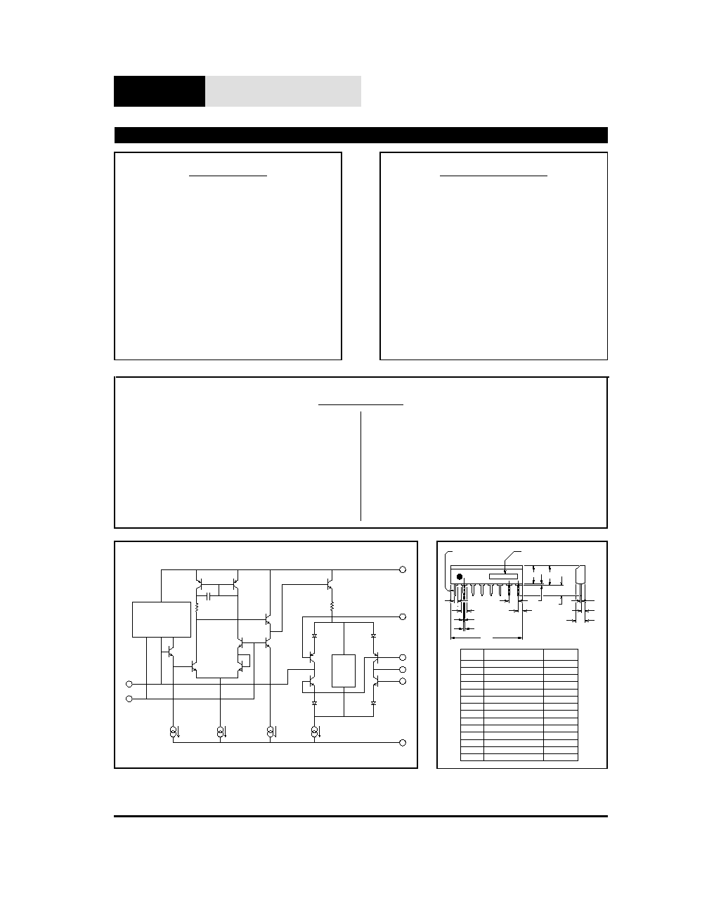
Figure 1. 2150 Series Equivalent Circuit Diagram
A
TYP.
ITEM
MILLIMETERS
INCHES
A
20.32 MAX.
1.1 MIN.
0.25
2.54
1.27 MAX.
B
C
D
E
F
0.8 MAX.
0.043 MIN.
0.02
+
0.01
0.1
0.05 MAX.
0.02 MIN.
0.2 MAX.
0.11
.008
+
0.227 MAX.
0.058 MAX.
0.01
.004
.002
+
0.126
.02
+
0.043 MIN.
G
H
I
J
K
0.51 MIN.
5.08 MAX.
2.8
.2
+
5.75 MAX.
0.25
+.10
L
M
N
3.2
1.1 MIN.
.5
+
1.5 MAX.
_
_
_
_
.04
_
_
_
.004
C
D
B
N
J
M
F
L
K
I
0.5
+
_ .1
H
G
E
PIN 1
THAT
MODEL NO.
Figure 2. 2150 Series Physical Outline
IC Voltage-Controlled
Amplifiers
THAT
2151, 2150A, 2155
FEATURES
∑
Wide Dynamic Range: >116 dB
∑
Wide Gain Range: >130 dB
∑
Exponential (dB) Gain Control
∑
Low Distortion: (0.008% @ 0 dB
gain, 0.035% @15dB gain)
∑
Wide Gain-Bandwidth: 6 MHz
∑
Low Cost: $2.20 in '000s (2155)
∑
Single In-Line Package
∑
Dual Gain-Control Ports (pos/neg)
APPLICATIONS
∑
Faders
∑
Panners
∑
Compressors
∑
Expanders
∑
Equalizers
∑
Filters
∑
Oscillators
∑
Automation Systems
Description
The THAT 2150 Series integrated-circuit voltage-
controlled amplifiers (VCAs) are high-performance
current-in/current-out devices with two opposing-
polarity, voltage-sensitive control ports. Based on
dbx
technology, they offer wide-range exponential
control of gain and attenuation with low signal dis-
tortion. The parts are housed in a space-efficient,
plastic 8-pin single-in-line (SIP) package, and re-
quire minimal support circuitry. Fabricated in a
super low-noise process utilizing high h
FE
, comple-
mentary NPN/PNP pairs, the 2150 Series VCAs
combine high gain-bandwidth product with low
noise, low distortion, and low offset to offer discrete
performance at IC prices. They are available in
three grades, selected for distortion, allowing the
user to optimize cost vs. performance.
dbx
is a registered trademark of Carillon Electronics Corporation
THAT Corporation; 734 Forest Street; Marlborough, Massachusetts 01752; USA
Tel: (508) 229-2500; Fax: (508) 229-2590; Web: http://www.thatcorp.com
OBSOLET
E
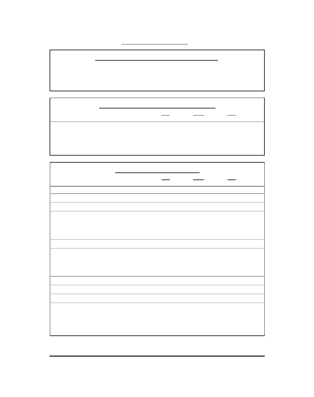
SPECIFICATIONS
1
Absolute-Maximum Ratings (T
A
= 25∞C)
Positive Supply Voltage (V
CC
)
+18 V
Negative Supply Voltage (V
EE
)
-18 V
Supply Current (I
CC
)
10 mA
Power Dissipation (P
D
) (T
A
= 75∞C)
330 mW
Operating Temperature Range (T
OP
)
-20 to +75∞C
Storage Temperature Range (T
ST
)
-40 to +125∞C
Recommended Operating Conditions
2151
2150A
2155
Parameter
Symbol
Conditions
Min
Typ
Max
Min
Typ
Max
Min
Typ
Max
Units
Positive Supply Voltage
V
CC
+5
+12
+15
+5
+12
+15
+5
+12
+15
V
Negative Supply Voltage
V
EE
-5
-12
-15
-5
-12
-15
-5
-12
-15
V
Bias Current
I
SET
V
CC
-V
EE
= 24 V
--
2.4
4
--
2.4
4
--
2.4
4
mA
Signal Current
I
IN
+I
OUT
I
SET
= 2.4 mA
--
175
750
--
175
750
--
125
550
µ
Arms
Electrical Characteristics
2
2151
2150A
2155
Parameter
Symbol
Conditions
Min
Typ
Max
Min
Typ
Max
Min
Typ
Max
Units
Supply Current
I
CC
No Signal
--
2.4
4
--
2.4
4
--
2.4
4
mA
Equiv. Input Bias Current
I
B
No Signal
--
5
8
--
5
8
--
5
8
nA
Input Offset Voltage
V
OFF(IN)
No Signal
--
+10
--
--
+10
--
--
+10
--
mV
Output Offset Voltage
V
OFF(OUT)
R
out
=20 k
0 dB gain
--
1
3
--
1
3
--
1
3
mV
+15 dB gain
--
2
3
--
2
3
--
2
3
mV
+40 dB gain
--
5
15
--
7
15
--
10
15
mV
Gain Cell Idling Current
I
IDLE
--
20
--
--
20
--
--
20
--
µ
A
Gain-Control Constant
T
A
=25∞C (T
CHIP
35∞C)
-60 dB < gain < +40 dB
E
C+
/Gain (dB)
Pins 2 & 4 (Fig. 14)
6.0
6.1
6.2
6.0
6.1
6.2
6.0
6.1
6.2
mV/dB
E
C-
/Gain (dB)
Pin 3
-6.0
-6.1
-6.2
-6.0
-6.1
-6.2
-6.0
-6.1
-6.2
mV/dB
Gain-control TempCo
E
C
/
T
CHIP
Ref T
CHIP
= 27∞C
--
+0.33
--
--
+0.33
--
--
+0.33
--
%/∞C
Gain-Control Linearity
-60 to +40 dB gain
--
0.5
2
--
0.5
2
--
0.5
2
%
Off Isolation (Fig. 14)
E
C+
=-360mV, E
C-
=+360mV
110
115
--
110
115
110
115
--
dB
Output Noise
e
n(OUT)
20 Hz-20 kHz
R
out
= 20k
0 dB gain
--
-98
-97
--
-98
-96
--
-98
-96
dBV
+15 dB gain
--
-88
-86
--
-88
-86
--
-88
-86
dBV
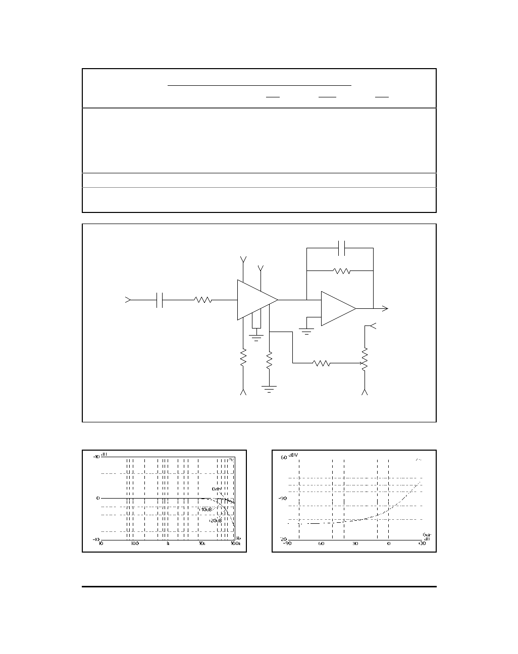
1. All specifications subject to change without notice.
2. Unless otherwise noted, TA=25∞C, VCC = +15V, VEE= -15V. Test circuit is as shown in Figure 3. SYMADJ is ad-
justed for minimum THD @ Vin=1 V, 1 kHz, 0 dB gain.
THAT Corporation; 734 Forest Street; Marlborough, Massachusetts 01752; USA
Tel: (508) 229-2500; Fax: (508) 229-2590; Web: http://www.thatcorp.com
Page 2
2150 Series IC VCAs
OBSOLET
E
Electrical Characteristics (Cont'd.)
2151
2150A
2155
Parameter
Symbol
Conditions
Min
Typ
Max
Min
Typ
Max
Min
Typ
Max
Units
Total Harmonic Distortion
THD
I
IN
+ I
OUT
= 180
µ
A, 1 kHz
0 dB gain
--
0.004 0.02
--
0.005 0.03
--
--
--
%
±
15 dB gain
--
0.025 0.045
--
0.05
0.07
--
--
--
%
I
IN
+ I
OUT
= 150
µ
A, 1 kHz
0 dB gain
--
--
--
--
--
--
--
0.006 0.03
%
±
15 dB gain
--
--
--
--
--
--
--
0.05
0.07
%
Symmetry Control Voltage
V
SYM
A
V
= 0 dB, THD < 0.07%
-1.6
0
+1.6
-2
0
+2
-2.5
0
+2.5
mV
Gain at 0 V Control Voltage
E
C≠
= 0 mV
-0.1
0.0
+0.1
-0.15
0.0
+0.15
-0.2
0.0
+0.2
dB
Ec+
Ec+
Ec-
OUT
-IN
V-
GND
V+
-
+
Ec-
10u
LF351
47p
20k
50k
ADJ
SYM
150k
51
5.1k
20k
+15V
-15V
-15V
+15V
OUTPUT
Rsym
INPUT
1
5
6
2
4
8
3
7
300k (2155)
390k (2150A)
470k (2151)
Figure 3. Typical Application Circuit
Figure 4. Frequency Response Vs. Gain (2150A)
2150
Series
VCA
Figure 5. Noise (20kHz NBW) Vs. Gain (2150A)
THAT Corporation; 734 Forest Street; Marlborough, Massachusetts 01752; USA
Tel: (508) 229-2500; Fax: (508) 229-2590; Web: http://www.thatcorp.com
Rev. 10/25/96
Page 3

OBSOLET
E
Theory of Operation
The THAT 2150 Series VCAs are designed for high
performance in audio-frequency applications requiring
exponential gain control, low distortion, wide dynamic
range and low dc bias modulation. These parts control
gain by converting an input current signal to a bipolar
logged voltage, adding a dc control voltage, and re-con-
verting the summed voltage back to a current through
a bipolar antilog circuit.
Figure 6 presents a considerably simplified internal
circuit diagram of the IC. The ac input signal current
flows in pin 1, the input pin. The internal op amp
works to maintain pin 1 at a virtual ground potential
by driving the emitters of Q1 and (through the Voltage
Bias Generator) Q3. For positive input currents (I
in
de-
fined as flowing into pin 1), the op amp drives the emit-
ter of Q1 negative, turning off its collector current,
while simultaneously driving the emitter of Q3 nega-
tive, turning it on. The input signal current, therefore,
is forced to flow through Q3 and D3.
Logging & Antilogging
Because the voltage across a base-emitter junction
is logarithmic with collector current, the voltage from
the base of Q3 to the cathode of D3 is proportional to
the log of the positive input current. The voltage at the
cathodes of D3 and D4 is therefore proportional to the
log of the positive input currents plus the voltage at
pin 3, the negative control port. Mathematically,
V
3
=
E
C
-
-
2V
T
ln
I
C3
I
S
,
where V
3
is the voltage at the junction of D3 and D4;
V
T
is the thermal voltage,
kT
q
; I
C3
is the collector cur-
rent of Q3; and I
S
is the reverse-saturation current of
Q3. It is assumed that D3 matches Q3 (and will be as-
sumed that they match Q4 and D4, as well).
In typical applications (see Figure 3, Page 3), pin 4
is connected to a voltage source at ground or nearly
ground potential. Pin 8 is connected to a virtual
ground (usually the inverting input of an op amp with
negative feedback around it). With pin 4 near ground,
and pin 8 at virtual ground, the voltage at the cathodes
of D3 and D4 will cause an exponentially-related cur-
rent to flow in D4 and Q4, and out via pin 8. A similar
equation governs this behavior:
V
3
=
E
C
+
-
2V
T
ln
I
C4
I
S
.
Exponential Gain Control
The similarity between the two preceeding equations
begs further exploration. Accordingly:
V
3
=
E
C
+
-
2V
T
ln
I
C4
I
S
=
E
C
-
-
2V
T
ln
I
C3
I
S
E
C
+
-
E
C
-
=
2V
T
ln
I
C4
I
S
-
2V
T
ln
I
C3
I
S
=
2V
T
ln
I
C4
I
C3
.
Rearranging terms,
I
C4
=
I
C3
e
E
C
+
-
E
C
-
2V
T
.
If pin 3 and pin 4 are at ground potential, the cur-
rent in Q4/D4 will precisely mirror that in Q3/D3.
When pin 3 is positive with respect to pin 4, the voltage
across the base-emitter junction of Q3 is higher than
that across the base-emitter junction of Q4, so the
Q4/D4 current remains proportional to, but less than,
the current in Q3/D3. In the same manner, a negative
voltage at pin 3 with respect to pin 4 causes the
Q4/D4 current to be proportional to, but greater than
that in Q3/D3.
The ratio of currents is exponential with the differ-
ence in the voltages E
C+
and E
C≠
, providing convenient
"deci-linear" control. Mathematically, this is:
A
V
=
I
C4
I
C3
=
e
E
C
+
-
E
C
-
2V
T
, where A
V
is the current gain.
For pin 4 at or very near ground, at room tempera-
ture (25∞C), allowing for a 10∞C internal temperature
rise, and converting to a base of 10 for the exponential,
this reduces to:
-
+
Q1
Q4
Q3
Q2
D3
D1
5
4
8
3
1
2
(SYM)
V-
IN
Ec+
Ec+
OUT
Ec-
Generator
Bias
Voltage
D2
D4
V3
Iin
Figure 6. Simplified Internal Circuit Diagram
THAT Corporation; 734 Forest Street; Marlborough, Massachusetts 01752; USA
Tel: (508) 229-2500; Fax: (508) 229-2590; Web: http://www.thatcorp.com
Page 4
2150 Series IC VCAs
OBSOLET
E
A
V
=
10
-
EC
-
0.122
.
When pin 3 is at O V, the current ratio is unity.
When pin 3 is at +122 mV, the output current (Q4) is
10 times (20 dB) less than the input current. At
≠122 mV, the output current is 10 times (20 dB)
greater than the input current. Another way of ex-
pressing this relationship is:
Gain
=
-
E
C
-
0.0061
, where Gain is the gain in decibels.
Negative Input Currents
For negative input currents, Q1/D1 operate with
Q2/D2 to mirror the lower-half-core behavior. Pin 2 is
normally at or very near ground (see the section below
on Symmetry Adjustment for more detail), so the same
gain scaling applied to the base of Q3 is applied to the
base of Q2. The polarity (positive/negative, in dB) of
the gain is the same for the top pair versus the bottom
pair of the four "core" transistors because their sexes
(NPN/PNP) are inverted in the top versus the bottom,
while the bases are cross-connected between the input
(left) half and the output (right) half of each pair.
The resulting control over gain is extremely consis-
tent from unit to unit, since it derives from the physics
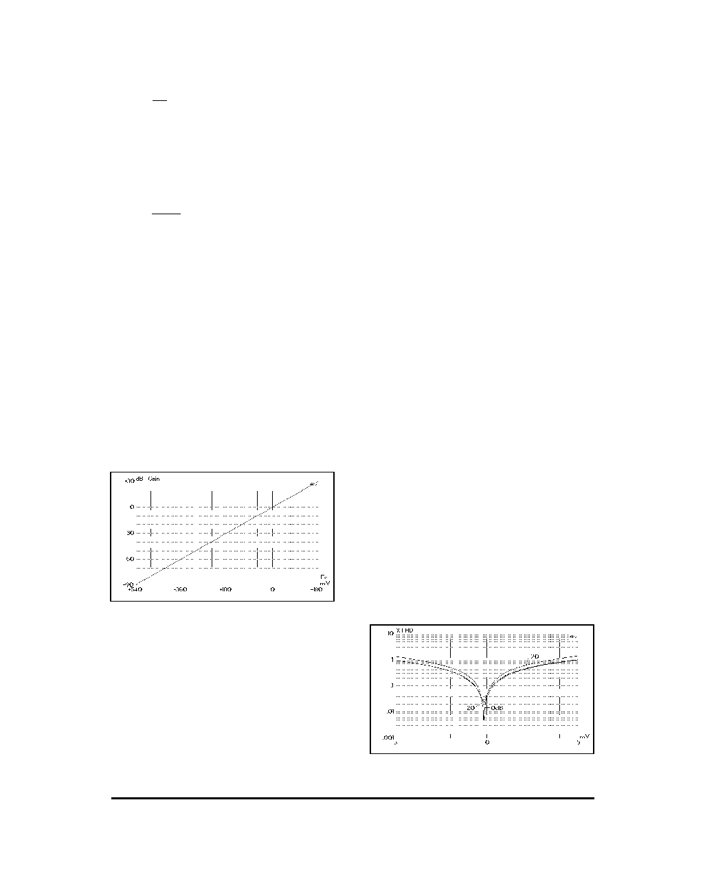
of semiconductors. Figure 7 shows actual data from a
typical 2150 Series VCA, taken at 25∞C.
Core Bias Currents
A quiescent bias current in the core transistors is
established by the Voltage Bias Generator shown in
Figure 6. This current acts like crossover bias in the
output stage of a complementary class AB power am-
plifier, smoothing the transition between turning on
the top (PNP) pair and the bottom (NPN) pair of transis-
tors in the core. This lowers distortion greatly at some
cost to noise performance, as the current noise of the
core transistors (which run at approximately 20
µ
A) is
the dominant noise source in the 2150 Series VCAs.
Transistor Matching
The bias current flows downwards in the core (from
Q1 to Q3, and from Q2 to Q4) so long as there is good
matching between all four compound transistors (tran-
sistors plus diodes). Mismatches will cause a dc output
current to flow in pin 8, which will ultimately manifest
itself as a dc offset voltage. Static offsets are of little
consequence in most audio applications, but any mis-
match-caused dc output current will be modulated by
gain commands, and may become audible as "thumps"
if large, fast gain changes are commanded in the pres-
ence of significant mismatches.
Transistor matching also affects distortion. If the
top half of the gain cell is perfectly matched, while the
bottom half is slightly off, then the gain commanded by
the voltage at pin 3 will affect the two halves of the core
differently. Since positive and negative halves of ac
input signals are handled by separate parts of the core,
this gives rise to even-order distortion products.
Symmetry Adjustment
The monolithic construction of the devices assures
relatively good matching between the paired transis-
tors, but even small V
BE
mismatches can cause unac-
ceptable asymmetries in the output. For this reason,
the bases of Q1 and Q4 are brought out separately to
pin 2 and pin 4, respectively. This allows a small static
voltage differential to be applied to the two bases. The
applied voltage must be set to equal the sum of the V
BE
mismatches around the core (which varies from sample
to sample). Figure 3 (Page 3) includes a typical circuit
to apply this symmetry voltage. R
SYM
controls primarily
even-order harmonic distortion, and is usually ad-
justed for minimum THD at the output. Figure 8 plots
THD vs. the voltage between pins 2 and 4 (the two E
C+
ports) for various gain settings of a typical part.
Opposite Polarity Control
As may be seen from the mathematics, the bases of
Q1 and Q4 can also be used as an additional control
Figure 7. Gain Versus Control Voltage (Pin 3) at 25∞C
Figure 8. Typical THD Versus Symmetry Voltage
THAT Corporation; 734 Forest Street; Marlborough, Massachusetts 01752; USA
Tel: (508) 229-2500; Fax: (508) 229-2590; Web: http://www.thatcorp.com
Rev. 10/25/96
Page 5