T H A T
C o r p o r a t i o n
COMPENSATION
BIAS CURRENT
5
6
1
7
4
8
3
2
PLIER
MULTI-
Vbe
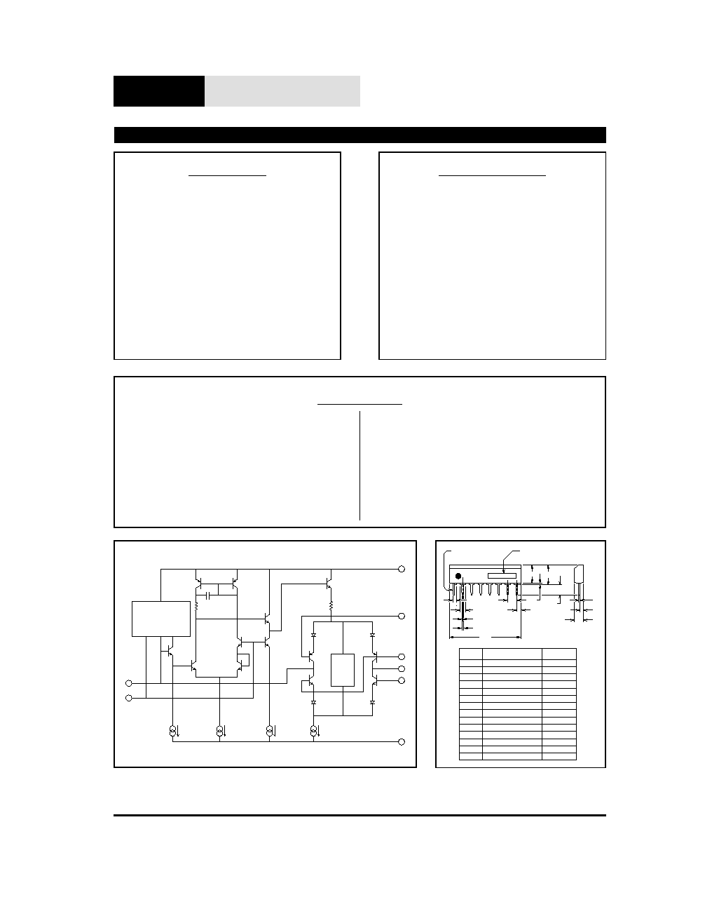
Figure 1. 2150 Series Equivalent Circuit Diagram
A
TYP.
ITEM
MILLIMETERS
INCHES
A
20.32 MAX.
1.1 MIN.
0.25
2.54
1.27 MAX.
B
C
D
E
F
0.8 MAX.
0.043 MIN.
0.02
+
0.01
0.1
0.05 MAX.
0.02 MIN.
0.2 MAX.
0.11
.008
+
0.227 MAX.
0.058 MAX.
0.01
.004
.002
+
0.126
.02
+
0.043 MIN.
G
H
I
J
K
0.51 MIN.
5.08 MAX.
2.8
.2
+
5.75 MAX.
0.25
+.10
L
M
N
3.2
1.1 MIN.
.5
+
1.5 MAX.
_
_
_
_
.04
_
_
_
.004
C
D
B
N
J
M
F
L
K
I
0.5
+
_ .1
H
G
E
PIN 1
THAT
MODEL NO.
Figure 2. 2150 Series Physical Outline
IC Voltage-Controlled
Amplifiers
THAT
2151, 2150A, 2155
FEATURES
�
Wide Dynamic Range: >116 dB
�
Wide Gain Range: >130 dB
�
Exponential (dB) Gain Control
�
Low Distortion: (0.008% @ 0 dB
gain, 0.035% @15dB gain)
�
Wide Gain-Bandwidth: 6 MHz
�
Low Cost: $2.20 in '000s (2155)
�
Single In-Line Package
�
Dual Gain-Control Ports (pos/neg)
APPLICATIONS
�
Faders
�
Panners
�
Compressors
�
Expanders
�
Equalizers
�
Filters
�
Oscillators
�
Automation Systems
Description
The THAT 2150 Series integrated-circuit voltage-
controlled amplifiers (VCAs) are high-performance
current-in/current-out devices with two opposing-
polarity, voltage-sensitive control ports. Based on
dbx
technology, they offer wide-range exponential
control of gain and attenuation with low signal dis-
tortion. The parts are housed in a space-efficient,
plastic 8-pin single-in-line (SIP) package, and re-
quire minimal support circuitry. Fabricated in a
super low-noise process utilizing high h
FE
, comple-
mentary NPN/PNP pairs, the 2150 Series VCAs
combine high gain-bandwidth product with low
noise, low distortion, and low offset to offer discrete
performance at IC prices. They are available in
three grades, selected for distortion, allowing the
user to optimize cost vs. performance.
dbx
is a registered trademark of Carillon Electronics Corporation
THAT Corporation; 734 Forest Street; Marlborough, Massachusetts 01752; USA
Tel: (508) 229-2500; Fax: (508) 229-2590; Web: http://www.thatcorp.com
SPECIFICATIONS
1
Absolute-Maximum Ratings (T
A
= 25�C)
Positive Supply Voltage (V
CC
)
+18 V
Negative Supply Voltage (V
EE
)
-18 V
Supply Current (I
CC
)
10 mA
Power Dissipation (P
D
) (T
A
= 75�C)
330 mW
Operating Temperature Range (T
OP
)
-20 to +75�C
Storage Temperature Range (T
ST
)
-40 to +125�C
Recommended Operating Conditions
2151
2150A
2155
Parameter
Symbol
Conditions
Min
Typ
Max
Min
Typ
Max
Min
Typ
Max
Units
Positive Supply Voltage
V
CC
+5
+12
+15
+5
+12
+15
+5
+12
+15
V
Negative Supply Voltage
V
EE
-5
-12
-15
-5
-12
-15
-5
-12
-15
V
Bias Current
I
SET
V
CC
-V
EE
= 24 V
--
2.4
4
--
2.4
4
--
2.4
4
mA
Signal Current
I
IN
+I
OUT
I
SET
= 2.4 mA
--
175
750
--
175
750
--
125
550
�
Arms
Electrical Characteristics
2
2151
2150A
2155
Parameter
Symbol
Conditions
Min
Typ
Max
Min
Typ
Max
Min
Typ
Max
Units
Supply Current
I
CC
No Signal
--
2.4
4
--
2.4
4
--
2.4
4
mA
Equiv. Input Bias Current
I
B
No Signal
--
5
8
--
5
8
--
5
8
nA
Input Offset Voltage
V
OFF(IN)
No Signal
--
+10
--
--
+10
--
--
+10
--
mV
Output Offset Voltage
V
OFF(OUT)
R
out
=20 k
0 dB gain
--
1
3
--
1
3
--
1
3
mV
+15 dB gain
--
2
3
--
2
3
--
2
3
mV
+40 dB gain
--
5
15
--
7
15
--
10
15
mV
Gain Cell Idling Current
I
IDLE
--
20
--
--
20
--
--
20
--
�
A
Gain-Control Constant
T
A
=25�C (T
CHIP
35�C)
-60 dB < gain < +40 dB
E
C+
/Gain (dB)
Pins 2 & 4 (Fig. 14)
6.0
6.1
6.2
6.0
6.1
6.2
6.0
6.1
6.2
mV/dB
E
C-
/Gain (dB)
Pin 3
-6.0
-6.1
-6.2
-6.0
-6.1
-6.2
-6.0
-6.1
-6.2
mV/dB
Gain-control TempCo
E
C
/
T
CHIP
Ref T
CHIP
= 27�C
--
+0.33
--
--
+0.33
--
--
+0.33
--
%/�C
Gain-Control Linearity
-60 to +40 dB gain
--
0.5
2
--
0.5
2
--
0.5
2
%
Off Isolation (Fig. 14)
E
C+
=-360mV, E
C-
=+360mV
110
115
--
110
115
110
115
--
dB
Output Noise
e
n(OUT)
20 Hz-20 kHz
R
out
= 20k
0 dB gain
--
-98
-97
--
-98
-96
--
-98
-96
dBV
+15 dB gain
--
-88
-86
--
-88
-86
--
-88
-86
dBV
1. All specifications subject to change without notice.
2. Unless otherwise noted, TA=25�C, VCC = +15V, VEE= -15V. Test circuit is as shown in Figure 3. SYMADJ is ad-
justed for minimum THD @ Vin=1 V, 1 kHz, 0 dB gain.
THAT Corporation; 734 Forest Street; Marlborough, Massachusetts 01752; USA
Tel: (508) 229-2500; Fax: (508) 229-2590; Web: http://www.thatcorp.com
Page 2
2150 Series IC VCAs
Electrical Characteristics (Cont'd.)
2151
2150A
2155
Parameter
Symbol
Conditions
Min
Typ
Max
Min
Typ
Max
Min
Typ
Max
Units
Total Harmonic Distortion
THD
I
IN
+ I
OUT
= 180
�
A, 1 kHz
0 dB gain
--
0.004 0.02
--
0.005 0.03
--
--
--
%
�
15 dB gain
--
0.025 0.045
--
0.05
0.07
--
--
--
%
I
IN
+ I
OUT
= 150
�
A, 1 kHz
0 dB gain
--
--
--
--
--
--
--
0.006 0.03
%
�
15 dB gain
--
--
--
--
--
--
--
0.05
0.07
%
Symmetry Control Voltage
V
SYM
A
V
= 0 dB, THD < 0.07%
-1.6
0
+1.6
-2
0
+2
-2.5
0
+2.5
mV
Gain at 0 V Control Voltage
E
C�
= 0 mV
-0.1
0.0
+0.1
-0.15
0.0
+0.15
-0.2
0.0
+0.2
dB
Ec+
Ec+
Ec-
OUT
-IN
V-
GND
V+
-
+
Ec-
10u
LF351
47p
20k
50k
ADJ
SYM
150k
51
5.1k
20k
+15V
-15V
-15V
+15V
OUTPUT
Rsym
INPUT
1
5
6
2
4
8
3
7
300k (2155)
390k (2150A)
470k (2151)
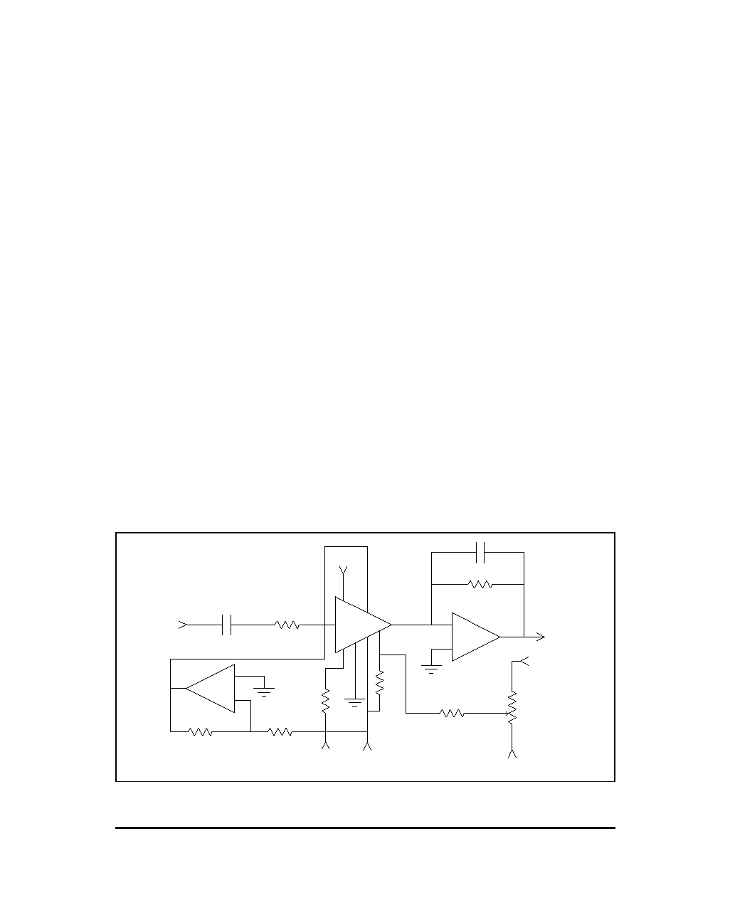
Figure 3. Typical Application Circuit
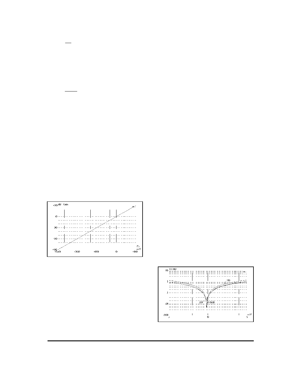
Figure 4. Frequency Response Vs. Gain (2150A)
2150
Series
VCA
Figure 5. Noise (20kHz NBW) Vs. Gain (2150A)
THAT Corporation; 734 Forest Street; Marlborough, Massachusetts 01752; USA
Tel: (508) 229-2500; Fax: (508) 229-2590; Web: http://www.thatcorp.com
Rev. 10/25/96
Page 3
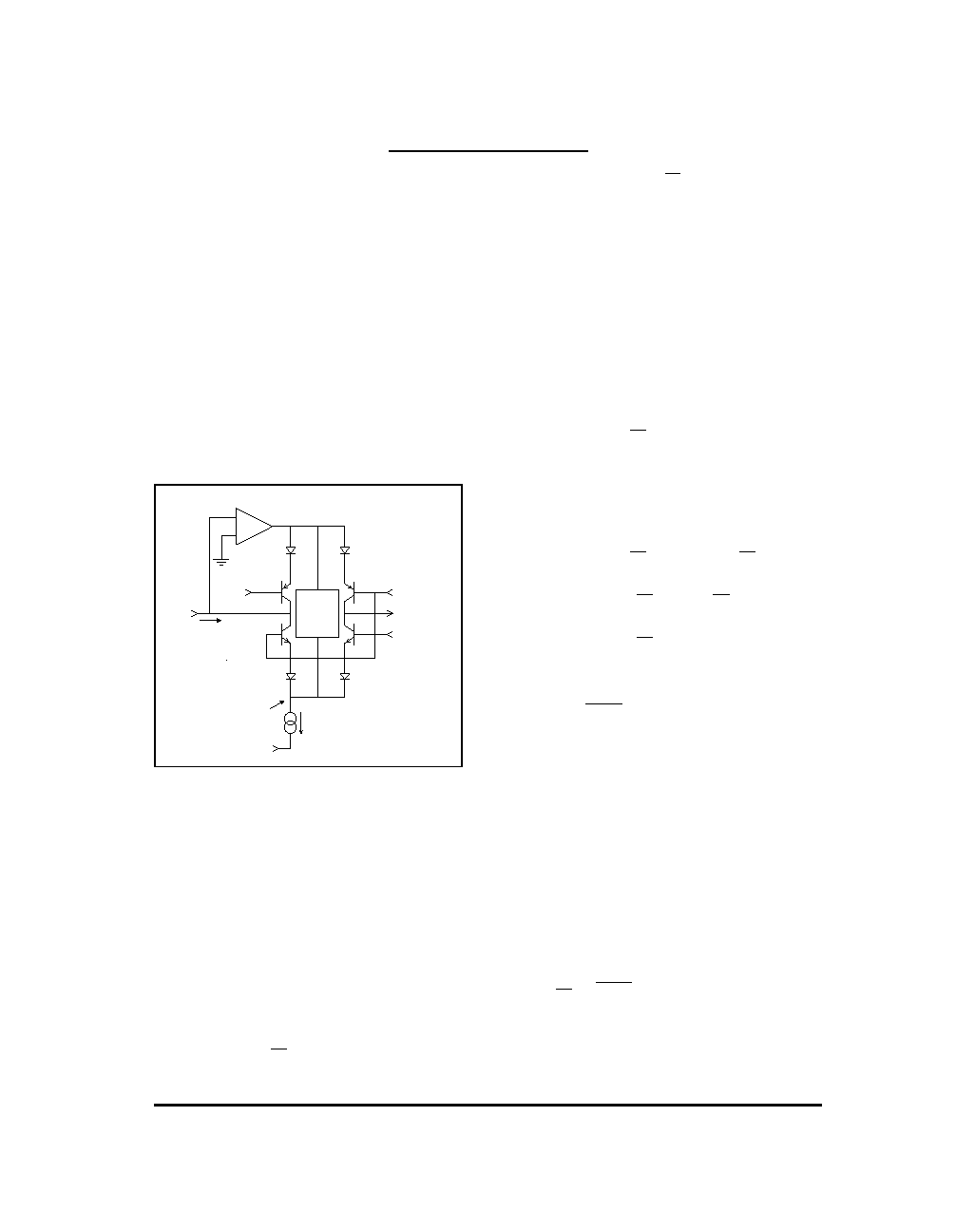
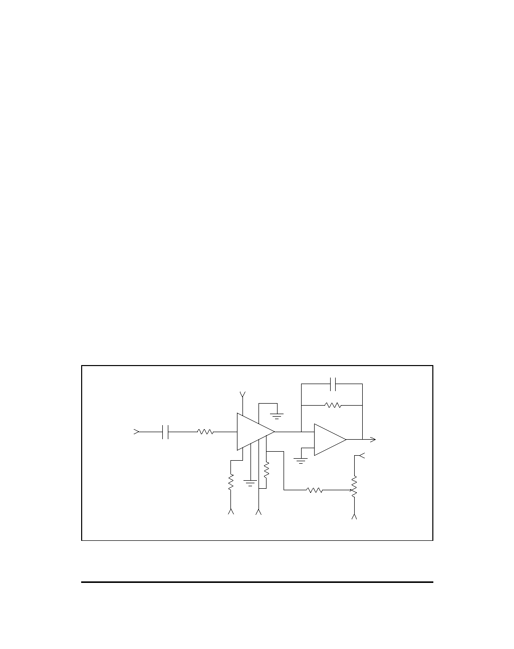
Theory of Operation
The THAT 2150 Series VCAs are designed for high
performance in audio-frequency applications requiring
exponential gain control, low distortion, wide dynamic
range and low dc bias modulation. These parts control
gain by converting an input current signal to a bipolar
logged voltage, adding a dc control voltage, and re-con-
verting the summed voltage back to a current through
a bipolar antilog circuit.
Figure 6 presents a considerably simplified internal
circuit diagram of the IC. The ac input signal current
flows in pin 1, the input pin. The internal op amp
works to maintain pin 1 at a virtual ground potential
by driving the emitters of Q1 and (through the Voltage
Bias Generator) Q3. For positive input currents (I
in
de-
fined as flowing into pin 1), the op amp drives the emit-
ter of Q1 negative, turning off its collector current,
while simultaneously driving the emitter of Q3 nega-
tive, turning it on. The input signal current, therefore,
is forced to flow through Q3 and D3.
Logging & Antilogging
Because the voltage across a base-emitter junction
is logarithmic with collector current, the voltage from
the base of Q3 to the cathode of D3 is proportional to
the log of the positive input current. The voltage at the
cathodes of D3 and D4 is therefore proportional to the
log of the positive input currents plus the voltage at
pin 3, the negative control port. Mathematically,
V
3
=
E
C
-
-
2V
T
ln
I
C3
I
S
,
where V
3
is the voltage at the junction of D3 and D4;
V
T
is the thermal voltage,
kT
q
; I
C3
is the collector cur-
rent of Q3; and I
S
is the reverse-saturation current of
Q3. It is assumed that D3 matches Q3 (and will be as-
sumed that they match Q4 and D4, as well).
In typical applications (see Figure 3, Page 3), pin 4
is connected to a voltage source at ground or nearly
ground potential. Pin 8 is connected to a virtual
ground (usually the inverting input of an op amp with
negative feedback around it). With pin 4 near ground,
and pin 8 at virtual ground, the voltage at the cathodes
of D3 and D4 will cause an exponentially-related cur-
rent to flow in D4 and Q4, and out via pin 8. A similar
equation governs this behavior:
V
3
=
E
C
+
-
2V
T
ln
I
C4
I
S
.
Exponential Gain Control
The similarity between the two preceeding equations
begs further exploration. Accordingly:
V
3
=
E
C
+
-
2V
T
ln
I
C4
I
S
=
E
C
-
-
2V
T
ln
I
C3
I
S
E
C
+
-
E
C
-
=
2V
T
ln
I
C4
I
S
-
2V
T
ln
I
C3
I
S
=
2V
T
ln
I
C4
I
C3
.
Rearranging terms,
I
C4
=
I
C3
e
E
C
+
-
E
C
-
2V
T
.
If pin 3 and pin 4 are at ground potential, the cur-
rent in Q4/D4 will precisely mirror that in Q3/D3.
When pin 3 is positive with respect to pin 4, the voltage
across the base-emitter junction of Q3 is higher than
that across the base-emitter junction of Q4, so the
Q4/D4 current remains proportional to, but less than,
the current in Q3/D3. In the same manner, a negative
voltage at pin 3 with respect to pin 4 causes the
Q4/D4 current to be proportional to, but greater than
that in Q3/D3.
The ratio of currents is exponential with the differ-
ence in the voltages E
C+
and E
C�
, providing convenient
"deci-linear" control. Mathematically, this is:
A
V
=
I
C4
I
C3
=
e
E
C
+
-
E
C
-
2V
T
, where A
V
is the current gain.
For pin 4 at or very near ground, at room tempera-
ture (25�C), allowing for a 10�C internal temperature
rise, and converting to a base of 10 for the exponential,
this reduces to:
-
+
Q1
Q4
Q3
Q2
D3
D1
5
4
8
3
1
2
(SYM)
V-
IN
Ec+
Ec+
OUT
Ec-
Generator
Bias
Voltage
D2
D4
V3
Iin
Figure 6. Simplified Internal Circuit Diagram
THAT Corporation; 734 Forest Street; Marlborough, Massachusetts 01752; USA
Tel: (508) 229-2500; Fax: (508) 229-2590; Web: http://www.thatcorp.com
Page 4
2150 Series IC VCAs
A
V
=
10
-
EC
-
0.122
.
When pin 3 is at O V, the current ratio is unity.
When pin 3 is at +122 mV, the output current (Q4) is
10 times (20 dB) less than the input current. At
�122 mV, the output current is 10 times (20 dB)
greater than the input current. Another way of ex-
pressing this relationship is:
Gain
=
-
E
C
-
0.0061
, where Gain is the gain in decibels.
Negative Input Currents
For negative input currents, Q1/D1 operate with
Q2/D2 to mirror the lower-half-core behavior. Pin 2 is
normally at or very near ground (see the section below
on Symmetry Adjustment for more detail), so the same
gain scaling applied to the base of Q3 is applied to the
base of Q2. The polarity (positive/negative, in dB) of
the gain is the same for the top pair versus the bottom
pair of the four "core" transistors because their sexes
(NPN/PNP) are inverted in the top versus the bottom,
while the bases are cross-connected between the input
(left) half and the output (right) half of each pair.
The resulting control over gain is extremely consis-
tent from unit to unit, since it derives from the physics
of semiconductors. Figure 7 shows actual data from a
typical 2150 Series VCA, taken at 25�C.
Core Bias Currents
A quiescent bias current in the core transistors is
established by the Voltage Bias Generator shown in
Figure 6. This current acts like crossover bias in the
output stage of a complementary class AB power am-
plifier, smoothing the transition between turning on
the top (PNP) pair and the bottom (NPN) pair of transis-
tors in the core. This lowers distortion greatly at some
cost to noise performance, as the current noise of the
core transistors (which run at approximately 20
�
A) is
the dominant noise source in the 2150 Series VCAs.
Transistor Matching
The bias current flows downwards in the core (from
Q1 to Q3, and from Q2 to Q4) so long as there is good
matching between all four compound transistors (tran-
sistors plus diodes). Mismatches will cause a dc output
current to flow in pin 8, which will ultimately manifest
itself as a dc offset voltage. Static offsets are of little
consequence in most audio applications, but any mis-
match-caused dc output current will be modulated by
gain commands, and may become audible as "thumps"
if large, fast gain changes are commanded in the pres-
ence of significant mismatches.
Transistor matching also affects distortion. If the
top half of the gain cell is perfectly matched, while the
bottom half is slightly off, then the gain commanded by
the voltage at pin 3 will affect the two halves of the core
differently. Since positive and negative halves of ac
input signals are handled by separate parts of the core,
this gives rise to even-order distortion products.
Symmetry Adjustment
The monolithic construction of the devices assures
relatively good matching between the paired transis-
tors, but even small V
BE
mismatches can cause unac-
ceptable asymmetries in the output. For this reason,
the bases of Q1 and Q4 are brought out separately to
pin 2 and pin 4, respectively. This allows a small static
voltage differential to be applied to the two bases. The
applied voltage must be set to equal the sum of the V
BE
mismatches around the core (which varies from sample
to sample). Figure 3 (Page 3) includes a typical circuit
to apply this symmetry voltage. R
SYM
controls primarily
even-order harmonic distortion, and is usually ad-
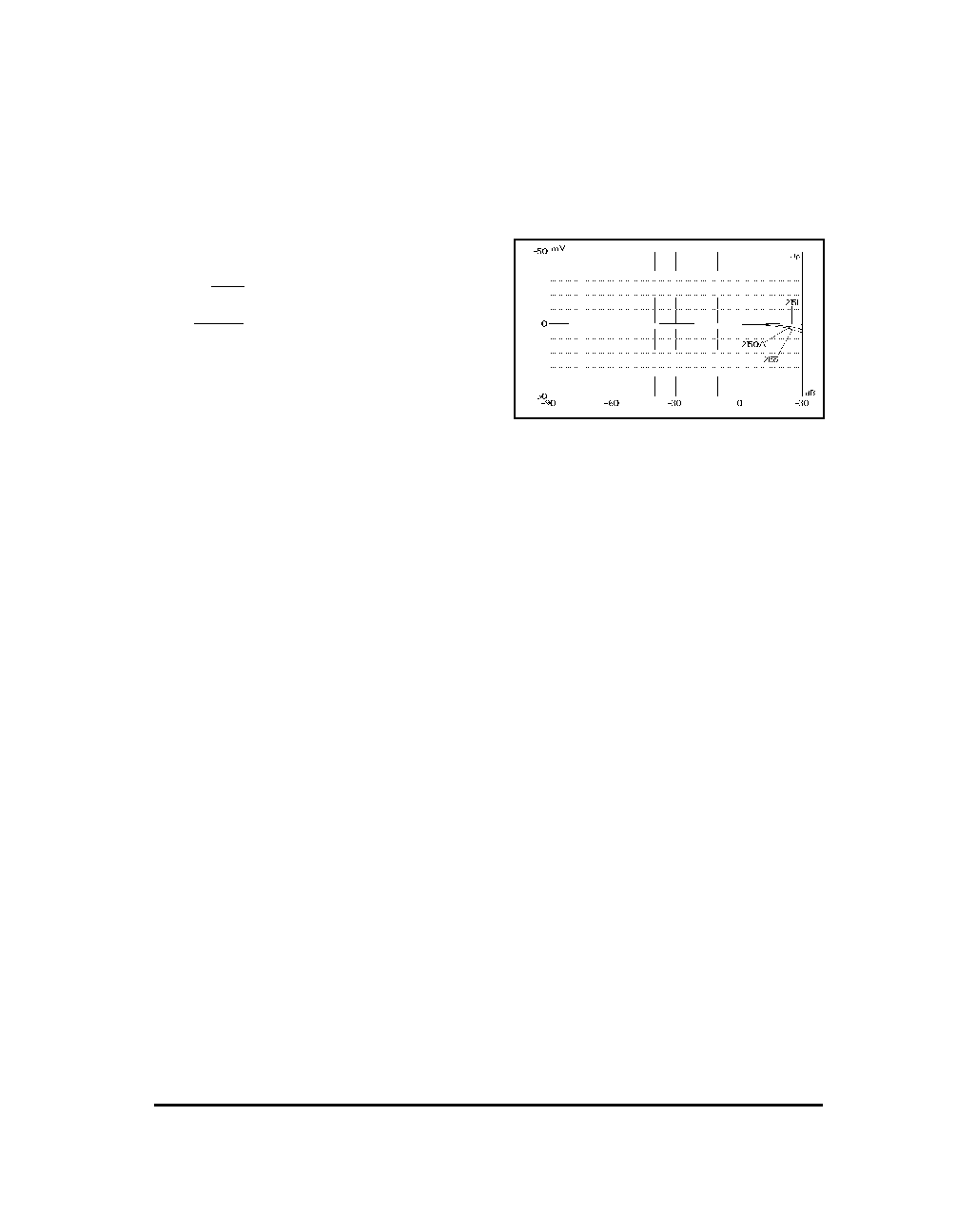
justed for minimum THD at the output. Figure 8 plots
THD vs. the voltage between pins 2 and 4 (the two E
C+
ports) for various gain settings of a typical part.
Opposite Polarity Control
As may be seen from the mathematics, the bases of
Q1 and Q4 can also be used as an additional control
Figure 7. Gain Versus Control Voltage (Pin 3) at 25�C
Figure 8. Typical THD Versus Symmetry Voltage
THAT Corporation; 734 Forest Street; Marlborough, Massachusetts 01752; USA
Tel: (508) 229-2500; Fax: (508) 229-2590; Web: http://www.thatcorp.com
Rev. 10/25/96
Page 5
port, with an opposite sense of control from that at
pin 3. To use this port, both pins must be driven with
the control voltage, while a small differential voltage is
accommodated between the two pins. (Figure 14,
Page 9, shows the typical connection.) Either pin 3, or
pins 2 and 4, or both ports together may be used for
gain control. Mathematically, this relationship is as fol-
lows:
A
V
=
10
EC
+-
EC
-
0.122
, where A
V
is the gain in volts/volt, or
Gain
=
E
c
+
-
E
c
-
0.0061
, where Gain is the gain in decibels.
Control Port Source Impedance
The control ports (pins 2 through 4) are connected
directly to the bases of the logging and/or antilogging
transistors. As was implied in the earlier discussion on
Logging and Antilogging (Page 4) the accuracy of the
logging and antilogging is dependent on the E
C+
and
E
C-
voltages being exactly as desired to control gain.
The base current in the transistors will follow the col-
lector currents, of course. Since the collector currents
are signal-related, the base currents will also be signal-
related. Should the source impedance of the control
voltage(s) be large, the signal-related base currents will
cause signal-related voltages to appear at the control
ports, which will interfere with precise logging and
antilogging, in turn causing distortion.
The 2150 Series VCAs are designed to be operated
with zero source impedance at pins 2 and 3, and a 50
source impedance at pin 4. (Pin 4 is intended for con-
nection to the symmetry control, hence the higher de-
sign-center source impedance.) One can estimate the
distortion caused by a specific, non-zero source imped-
ance by determining the base voltage modulation due
to signal current based on a core-transistor
of ap-
proximately 300 (NPN) or 100 (PNP), and converting the
resulting decibel gain modulation to a percentage.
Even 100
can spoil the good performance of these
parts at high signal levels.
DC Input Signals
Any dc currents in the feedback loop of the internal
op amp will show up as dc terms in the output signal,
and will be modulated by gain commands. Input bias
currents will cause a dc current to flow in the feedback
loop provided by the input side of the core. For this
reason, input bias currents in the internal op amp
must be kept very low. The bias current compensation
at the input stage provides excellent cancellation of the
bias current required by the input differential ampli-
fier. Of course, this good performance can be negated
by a dc current supplied from outside the VCA. To pre-
vent such dc terms, ac input coupling is strongly rec-
ommended. A plot of typical output offset voltage ver-
sus gain for the circuit of Figure 3 is shown in
Figure 9. (The LF351's offset was adjusted to 0 V for
this plot.)
Current Programming
The size of the current source at the bottom of the
core (Figure 6, Page 4) is programmed externally via
I
SET
, which is normally determined by a resistor from
pin 5 to V�. The voltage at pin 5 is typically �2.7 V. I
SET
divides into two portions: approximately 400
�
A is used
for internal biasing, and the rest is available for the
current source at the bottom of the core. I
SET
should
therefore be 400
�
A larger than the total of the peak
input and output signal currents.
Note that the output impedance of the internal op-
amp is approximately 2 k
, and under peak demands,
the sum of the input and output currents plus I
SET
must be supplied through this impedance, lowering the
voltage available to drive the core. For more informa-
tion, see the Power Supplies section on Page 8.
Headroom
Maximum signal currents are also limited by the
logarithmic characteristics of the core transistors. In
the 2150 Series, these devices are specially con-
structed to conform to an ideal log-linear curve over a
wide range of currents, but they reach their limit at ap-
proximately 1 mA. The symptom of failing log confor-
mance is increasing distortion with increasing current
levels. The onset of distortion is gradual at low current
levels, and then more rapid as current becomes high.
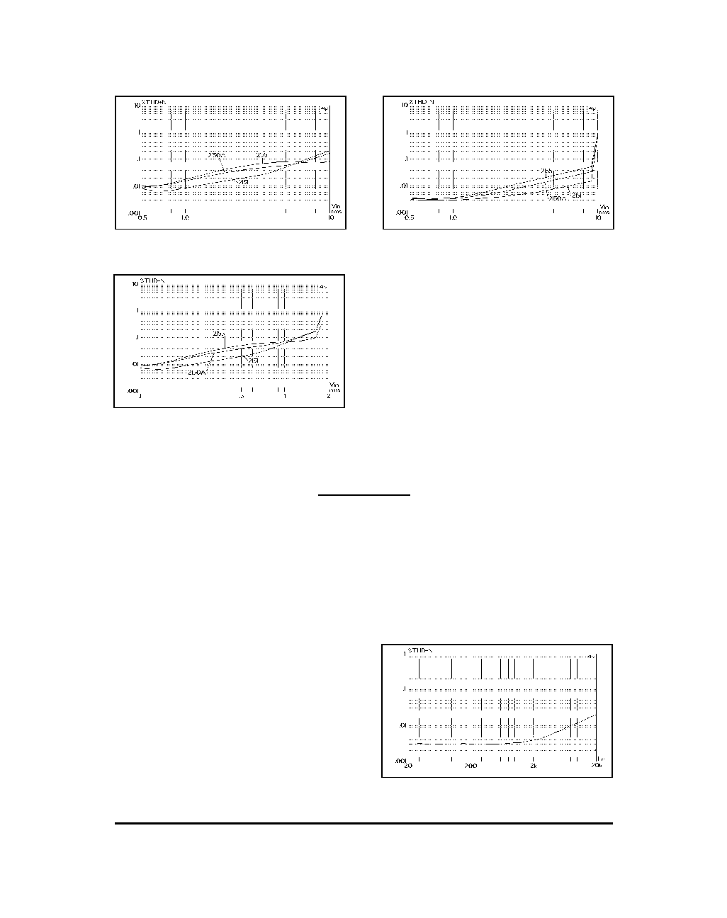
Figures 10 through 12 show distortion versus signal
level for the three parts in the 2150 Series for -15 dB,
0 dB, and +15 dB gain. The acceptable distortion will
determine the maximum signal level for a particular
design.
Figure 9. DC Offset Vs. Gain, After Symmetry
Adjustment
THAT Corporation; 734 Forest Street; Marlborough, Massachusetts 01752; USA
Tel: (508) 229-2500; Fax: (508) 229-2590; Web: http://www.thatcorp.com
Page 6
2150 Series IC VCAs
Applications
Input
As mentioned above, input and output signals are
currents, not voltages. While this often causes some
conceptual difficulty for designers first exposed to this
convention, the current input/output mode provides
great flexibility in application.
The input pin (pin 1) is a virtual ground with nega-
tive feedback provided internally (see Figure 6, Page 4).
The input resistor (shown as 20 k
in Figure 3, Page 3)
should be scaled to convert the available ac input volt-
age to a current within the linear range of the device.
(Peak input currents should be kept under 1 mA for
best distortion performance.) An additional consider-
ation is stability: the internal op amp is intended for
operation with source impedances of less than 30 k
at high frequencies. For most audio applications, this
will present no problem.
The choice of input resistor has an additional, sub-
tle effect on distortion. Since the feedback impedances
around the internal opamp (essentially Q1/D1 and
Q3/D3) are fixed, low values for the input resistor will
require more closed-loop gain from the opamp. Since
the open-loop gain naturally falls off at high frequen-
cies, asking for too much gain will lead to increased
high-frequency distortion. For best results, this resis-
tor should be kept to 10 k
or above. Distortion vs. fre-
quency for a 1 V signal at 0 dB gain with a 20 k
input
resistor is plotted in Figure 13.
The quiescent dc voltage level at the input is ap-
proximately +10 mV. As mentioned above, any dc input
currents will cause dc signals in the output which will
be modulated by gain, causing audible thump. There-
Figure 10. 1kHz THD+Noise Vs. Input, -15 dB Gain
Figure 11. 1kHz THD+Noise Vs. Level, 0 dB Gain
Figure 12. 1kHz THD+Noise Vs. Input, +15 dB Gain
Figure 13. THD Vs. Frequency, 0 dB Gain
THAT Corporation; 734 Forest Street; Marlborough, Massachusetts 01752; USA
Tel: (508) 229-2500; Fax: (508) 229-2590; Web: http://www.thatcorp.com
Rev. 10/25/96
Page 7

fore, capacitive coupling is almost mandatory for qual-
ity audio applications. Choose a capacitor which will
give acceptable low frequency performance for the ap-
plication.
Multiple signals may be summed by multiple resis-
tors, just as with an inverting op amp configuration. In
such a case, a single coupling capacitor may be located
next to pin 1 rather than multiple capacitors at the
driven ends of the summing resistors. However, take
care that the capacitor does not act as an antenna for
stray signals.
Output
The output pin (pin 8) is intended to be connected to
a virtual ground node, so that current flowing in it may
be converted to a voltage (see Figures 3, 14, & 15).
Choose the external op amp for good audio perfor-
mance. The feedback resistor should be chosen based
on the desired current-to-voltage conversion constant.
Since the input resistor determines the voltage-to-cur-
rent conversion at the input, the familiar ratio of R
f
/R
i
for an inverting op amp will determine the overall volt-
age gain when the VCA IC is set for 0 dB current gain.
Since the VCA performs best at settings near unity
gain, use the input and feedback resistors to provide
design-center gain or loss, if necessary.
A small feedback capacitor around the output op
amp is necessary to cancel the output capacitance of
the VCA. Without it, this capacitance will destabilize
most op amps. The capacitance at pin 8 is typically
30 pf.
Power Supplies
The positive supply is connected directly to pin 7.
No special bypassing is necessary, but it is good prac-
tice to include a small (~1
�
f) electrolytic close to the
VCA IC on the PCB. Performance is not particularly de-
pendent on supply voltage. The lowest permissible sup-
ply voltage is determined by the sum of the input and
output currents plus I
SET
, which must be supplied
through the resistor at the top of the core transistors
(see Figure 1) while still allowing enough voltage swing
to bias the internal op amp and the core transistors
themselves. This resistor is approximately 2 k
. Re-
ducing signal currents may help accommodate low
supply voltages.
The highest permissible supply voltage is fixed by
the process characteristics and internal power con-
sumption. +15 V is the nominal limit.
The negative supply terminal is intended to be con-
nected to a resistive current source, which determines
the current available for the core. As mentioned before,
this source must supply the sum of the input and out-
put signal currents, plus the bias to run the rest of the
IC. The minimum value for this current is 430
�
A over
the sum of the required signal currents. 2.4 mA is rec-
ommended for most pro audio applications where
+15 V supplies are common and headroom is import-
ant.
Higher bias levels are of limited value, partly be-
cause the resistor mentioned in the positive supply dis-
cussion must supply all the current devoted to the
core, and partly because the core transistors become
ineffective at logging and antilogging at currents over
1 mA.
Since pin 5 is intended as a current supply, not a
voltage supply, bypassing at pin 5 is not necessary.
Pin 6 is used as a ground reference for the VCA. The
non-inverting input of the internal op amp is con-
nected here, as are various portions of the internal bias
network. It may not be used as an additional input pin.
Voltage Control
The primary voltage-control pin is pin 3. This point
controls gain inversely with applied voltage: positive
voltage causes loss, negative voltage causes gain. As
described on Page 6, the current gain of the VCA is
unity when pin 3 is at 0 V with respect to pins 2 and 4,
and varies with voltage at approximately -6.1 mV/dB,
at room temperature.
As implied by the equation for A
V
(at the foot of
Page 4), the gain is sensitive to temperature, in propor-
tion to the amount of gain or loss commanded. The
constant of proportionality is 0.33% of the decibel gain
commanded, per degree Celsius, referenced to 27
�
C
(300
�
K). This means that at 0 dB gain, there is no
change in gain with temperature. However, at -122 mV,
the gain will be +20 dB at room temperature, but will
be 20.66 dB at a temperature 10�C lower. The formula
is:
Gain
=
E
C
+
-
E
C
-
(
0.0061
)
(
1
+
0.0033
)
T
,
where E
C
is in volts, and
T is the difference between
the actual temperature and room temperature (25�C).
For most audio applications, this change with tem-
perature is of little consequence. However, if necessary,
it may be compensated by a resistor which varies its
value by .33%/�C. Such parts are available from RCD
Components, Inc, 3301 Bedford St., Manchester, NH,
USA [(603) 669-0054], and KOA/Speer Electronics, PO
Box 547, Bradford, PA, 16701 USA [(814)362-5536].
When pin 3 is used for voltage control, pin 2 is con-
nected to ground and pin 4 is used to apply a small
THAT Corporation; 734 Forest Street; Marlborough, Massachusetts 01752; USA
Tel: (508) 229-2500; Fax: (508) 229-2590; Web: http://www.thatcorp.com
Page 8
2150 Series IC VCAs
symmetry voltage (<
�
2.5 mV) to correct for V
BE
mis-
matches within the VCA IC. For this purpose, the 2150
series devices were designed for optimum performance
with an impedance of approximately 50
at pin 4. A
trim pot is used to adjust the voltage between pin 4
and pin 2 as shown in Figure 3, Page 3. For supply
voltages other than shown, scale R
SYM
to provide the
required adjustment range.
It is also possible to use pin 2 and pin 4 together as
an opposite-sense voltage control port. A typical circuit
using this approach is shown in Figure 14. Pin 3 may
be grounded, and pin 2 driven against the symmetry-
adjustment voltage. The change in voltage at pin 4
does have a small effect on the symmetry voltage, but
this is of little practical consequence in most applica-
tions. Using the opposite sense of control can some-
times save an inverter in the control path.
It is also possible (and advantageous) to combine
both control ports with differential drive (see Fig-
ure 15). While the driving circuitry is more complex,
this configuration offers better performance at high
attentuation levels (<-90 dB) where the single-control-
port circuits begin to saturate Q1 (for E
C�
drive) or Q3
(for E
C+
drive). When either of these transistors satu-
rates, the internal opamp will accomodate the change
in current demand by responding with a small change
in its input offset voltage. This leads to an accumula-
tion of charge on the input capacitor, which in turn
can cause thump when the high attenuation is sud-
denly removed (e.g., when a muted channel is opened).
Differential control drive avoids the large dc levels oth-
erwise required to command high attenuation
(+610 mV for -100 dB gain at pin 3 alone, vs.
�
305 mV
when using both pin 3 and pins 2 and 4).
Control Port Drive Impedance
It has already been noted that the control port
should be driven by a low source impedance for mini-
mum distortion. This often suggests driving the control
port directly with an opamp (see below under Noise
Considerations). However, the closed-loop output im-
pedance of an opamp typically rises at high frequencies
due to falling loop gain. The output impedance is
therefore inductive at high frequencies. Excessive in-
ductance in the control port source impedance can
cause the VCA to oscillate internally. In such cases, a
51
resistor in series with a 1.5 nf capacitor from the
control port to ground will usually suffice to prevent
the instability.
Noise Considerations
It is second nature among good audio designers to
consider the effects of noisy devices on the signal path.
As is well known, this includes not only active devices
such as op amps and transistors, but extends to the
choice of impedance levels as well. High value resistors
have inherent thermal noise associated with them, and
the noise performance of an otherwise quiet circuit can
be easily spoiled by the wrong choice of impedance lev-
els.
Less well known, however, is the effect of noisy cir-
cuitry and high impedance levels in the control path of
Ec+
Ec+
Ec-
OUT
-IN
V-
GND
V+
-
+
240k
VCA
Series
2150
Rsym
Ec+
10u
LF351
47p
20k
50k
ADJ
SYM
51
5.1k
20k
+15V
-15V
-15V
+15V
OUTPUT
INPUT
1
5
6
2
4
8
3
7
2150
Series
VCA
300k (2155)
390k (2150A)
470k (2151)
Figure 14. Positive Control Port Using Pins 2 and 4
THAT Corporation; 734 Forest Street; Marlborough, Massachusetts 01752; USA
Tel: (508) 229-2500; Fax: (508) 229-2590; Web: http://www.thatcorp.com
Rev. 10/25/96
Page 9
voltage-control circuitry. The 2150 Series VCAs act like
double-balanced multipliers: when no signal is present
at the signal input, noise at the control input is re-
jected. So, when measuring noise (in the absence of
signal -- as most everyone does), even very noisy con-
trol circuitry often goes unnoticed. However, noise at
the control port of these parts will cause noise modula-
tion of the signal. This can become significant if care
is not taken to drive the control ports with quiet sig-
nals.
The 2150 Series VCAs have a small amount of in-
herent noise modulation because of its class AB bias-
ing scheme, where the shot noise in the core
transistors reaches a minimum with no signal, and in-
creases with the square root of the instantaneous sig-
nal current. However, in an optimum circuit, the noise
floor rises only to -94 dBV with a 50
�
A signal at unity
gain -- 4 dB of noise modulation. By contrast, if a
unity-gain connected, inverting 5534 opamp is used to
directly drive the control port, the noise floor will rise
to 92 dBV -- 6 dB of noise modulation.
To avoid excessive noise, one must take care to use
quiet electronics throughout the control-voltage cir-
cuitry. One useful technique is to process control volt-
ages at a multiple of the eventual control constant
(e.g., 61 mV/dB -- ten times higher than the VCA re-
quires), and then attenuate the control signal just be-
fore the final drive amplifier. With careful attention to
impedance levels, relatively noisy op amps may be
used for all but the final stage.
Closing Thoughts
The design and application of Voltage-Controlled
Amplifiers has traditionally been partly black art, in-
volving as much magic as science. We hope that the
foregoing discussion will help to de-mystify the subject.
THAT Corporation welcomes comments, questions
and suggestions regarding these devices, their design
and application. Please feel free to contact us with your
thoughts.
Ec+
Ec+
Ec-
OUT
-IN
V-
GND
V+
-
+
-
+
VCA
Series
2150
1k
1k
Rsym
Ec+
10u
LF351
47p
20k
50k
ADJ
SYM
150k
51
5.1k
20k
+15V
-15V
-15V
+15V
OUTPUT
INPUT
1
5
6
2
4
8
3
7
2150
Series
VCA
240k
300k (2155)
390k (2150A)
470k (2151)
Figure 15. Using Both Control Ports (Differential Drive)
THAT Corporation; 734 Forest Street; Marlborough, Massachusetts 01752; USA
Tel: (508) 229-2500; Fax: (508) 229-2590; Web: http://www.thatcorp.com
Page 10
2150 Series IC VCAs