THAT Corporation; 45 Sumner Street; Milford, Massachusetts 01757-1656; USA
Tel: +1 508 478 9200; Fax: +1 508 478 0990; Web: www.thatcorp.com
-
+
7
4
3
1
8
6
5
2
BIAS
CURRENT
COMP
1
V
BIAS
CURRENT
COMP
2
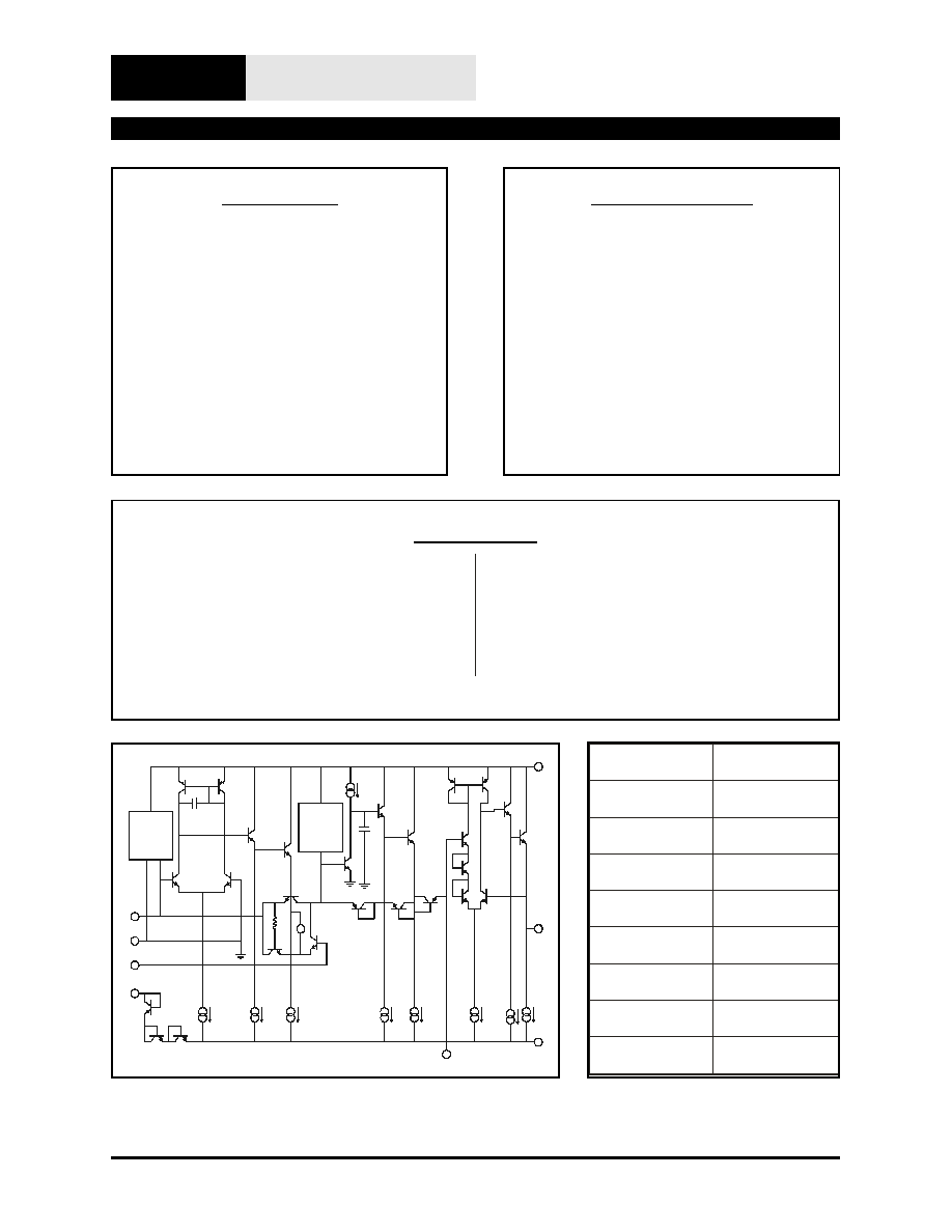
Fig ure 1. 2252 Equiv a lent Cir cuit Di a gram
Pin Name
SIP Pin
Input
1
I BIAS
2
Gnd
3
Sym
4
V-
5
Cap
6
Output
7
V+
8
Fig ure 2. 2252 Pin As sign ments
FEATURES
�
True RMS Re sponse
�
Wide Dy namic Range: >80 dB
�
High Crest Fac tor: 8 (1 dB er ror)
�
Wide Band width: to > 20 kHz
�
Log a rith mic Out put Scaling
�
Low Cost: $2.20 in '000s
�
Sin gle In-Line Pack age
�
Matches 2180 and 2181 Se ries
VCAs
APPLICATIONS
�
Me ters
�
Spec trum An a lyzers
�
Com pres sors
�
Ex panders
�
Os cil la tors
�
Psychoacoustic Modeling
�
Noise Mea sure ment
Description
The THAT 2252 in te grated-circuit rms-level de tec -
tor is de signed to con vert an ac in put cur rent into a
dc out put volt age. The out put is pro por tional to the
log of the true rms value of the in put sig nal. The
parts are housed in a space-efficient plas tic 8-pin
sin gle-in-line (SIP) pack age, and re quire min i mal
sup port cir cuitry. Based on dbx tech nol ogy and fab -
ri cated in a super low-noise pro cess, the 2252 com -
bines wide dy namic range with fre quency re sponse
to be yond 20 kHz. The log a rith mic out put is es pe -
cially con ve nient for au dio ap pli ca tions re quir ing
deci bel-linear scal ing. The in te gra tion time is ad -
just able via an ex ter nal R/C pair. With some ex ter -
nal cir cuitry, re sponse to dc is also pos si ble.
dbx
is a reg is tered trade mark of Car il lon Elec tron ics Cor po ra tion
T H A T
C o r p o r a t i o n
IC RMS-Level Detector
THAT
2252
Doc. 600032 Rev. 02

THAT Corporation; 45 Sumner Street; Milford, Massachusetts 01757-1656; USA
Tel: +1 508 478 9200; Fax: +1 508 478 0990; Web: www.thatcorp.com
Page 2
THAT 2252 RMS-Level De tec tor
SPECIFICATIONS
1
Ab so lute-Maximum Rat ings (TA = 25�C)
Pos i tive Sup ply Volt age (VCC)+18 V
Neg a tive Sup ply Volt age (VEE)
-18 V
Sup ply Cur rent (ICC)
10 mA
Power Dis si pa tion (PD)
330 mW
Op er ating Tem per a ture Range (TOP)
-20 to +75�C
Stor age Tem per a ture Range (TST)
-40 to +125�C
Rec om mended Op er ating Con di tions
Pa ram e ter
Sym bol
Con di tions
Min
Typ
Max
Units
Pos i tive Sup ply Volt age
V
CC
+4
+12
+15
V
Neg a tive Sup ply Volt age
V
EE
-4
-12
-15
V
Bias Set Cur rent
I
BIAS
15
24
50
�
A
Sig nal Cur rent
I
in
I
BIAS
= 24
�
A
--
--
1
mA
Tim ing Cur rent
I
T
1
7.5
50
�
A
Elec tri cal Characteristics
2
Pa ram e ter
Sym bol
Con di tions
Min
Typ
Max
Units
Sup ply Cur rent
I
CC
No Sig nal
--
1
3
mA
Equiv. In put Bias Cur rent
I
B
No Sig nal
--
5
8
nA
In put Off set Volt age
V
OFF(IN)
No Sig nal
0
+8
+16
mV
Sym me try Volt age
V
SYM
-2
8
+18
mV
Out put Scale Fac tor
E
O
/20log(I
in
/ I
in0
) 31.6nA<I
IN
<1mA
T
A
=25�C (T
CHIP
35�C) 6.0
6.1
6.2
mV/dB
In put Cur rent for 0V Out put
I
in0
I
I
3.5
BIAS
T
�
I
I
2.9
BIAS
T
�
I
I
2.4
BIAS
T
�
Out put Lin ear ity
f
IN
= 1kHz
1
�
A < I
in
< 100
�
A
--
0.1
--
dB
100nA < I
in
< 316
�
A
--
0.5
--
dB
31.6nA < I
in
< 1mA
--
1.0
--
dB
Crest Fac tor
1ms pulse rep e ti tion rate
0.2 dB er ror
--
3.5
--
0.5 dB er ror
--
5
--
1.0 dB er ror
--
8
--
Max i mum Fre quency for 1 dB ad di tional er ror
I
in
100
�
A
--
80
--
kHz
I
in
10
�
A
74
--
kHz
I
in
1
�
A
30
--
kHz
I
in
100nA
4
--
kHz
Fil tering Time Con stant
(.
)
026
C
I
T
T
s
Out put TempCo
E
0
/
T
CHIP
Re: T
CHIP
= 27
�
C
--
0.33
--
%
/
�
C
1. All spec i fi ca tions sub ject to change with out no tice.
2. Un less oth er wise noted, T
A
=25�C, V
CC
= +15V, V
EE
= -15V. Test cir cuit is as shown in Fig ure 4. SYM is ad justed for
min i mum rip ple at V
out
with V
in
=1 V
RMS
, 100 Hz.
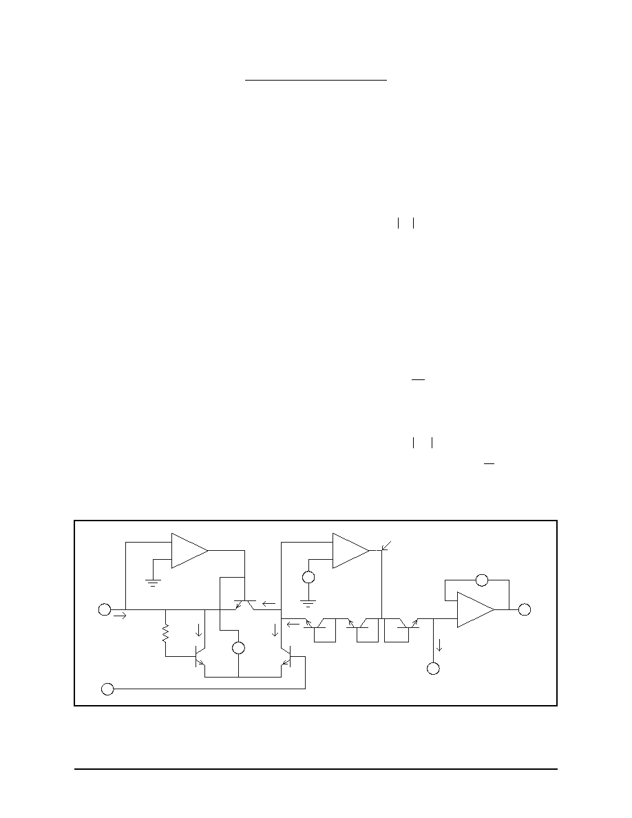
Theory of Operation
The THAT 2252 RMS-Level Detector is designed
for high performance in audio-frequency applica-
tions requiring logarithmic output, rms response,
and wide dynamic range. The parts compute rms
level by rectifying input current signals, converting
the resulting current waveform to a logarithmic
voltage, and applying this voltage to a log-domain
filter.
Current Rectification
Figure 3 presents a simplified internal circuit dia-
gram of the 2252. The input signal current, I
in
,
flows in pin 1, the input pin. OA1 drives the base
of Q3 and the emitter of Q1 (through V1) to main-
tain pin 1 at virtual ground potential. A negative
input current (flowing out of pin 1) will tend to
drive the inverting input of OA1 negative, driving
OA1's output positive, turning on Q3. V1 is de-
signed to cut off Q1 while Q3 is on. Therefore, neg-
ative input currents are forced to flow through the
collector-emitter of Q3.
Positive I
in
will drive OA1's output negative, cutting
off Q3 and turning on diode-connected transistor
Q1. Positive input current is thereby forced to flow
through the collector-emitter of Q1. Pin 4 is nor-
mally connected through a 20
resistor to ground
(see Figure 4, Typical Application Circuit, Page 4,
and
Symmetry Adjustment, Page 6), so the
base-emitter potential of Q2 is the same as that of
Q1. Therefore, the current in the collector of Q2
(I
C2
) will mirror that in the collector of Q1 (I
C1
),
which equals the positive input current.
Since the input impedance of OA2 is high, the cur-
rent in the emitter of Q4 (I
C4
), is the sum of the
currents I
C2
and I
C3
. The mirror action of Q1/Q2
reverses the positive input currents so that they
add to the negative input currents in Q4. The cur-
rent in Q4, therefore, is equal to the absolute value
of the input current.
Mathematically,
I
and I
I
C
in
in
in
C
C
in
in
in
I
I
I
I
I
I
3
1
2
0
0
0
0
0
=
=
=
>
-
>
,
,
,
,
,
0
.
But, I
I
I
I
I
C
C
C
C
C
4
3
2
3
1
=
+
=
+
=
>
-
<
I
I
I
I
in
in
in
in
,
,
0
0
= I
in
.
See Figure 3 for definitions of these currents.
Logging Action
OA2, together with Q4 and Q5, forms a log ampli-
fier. By using two diode-connected transistors in
the feedback loop of OA2, the 2252 produces a
voltage proportional to twice the log of IC4 at the
output of OA2. This voltage, V
log
, is therefore pro-
portional to the log of the square of the input cur-
rent, plus a bias voltage (V2).
Mathematically,
( )
V
V n
V
T
I
I
C
S
log
=
+
2
1
4
2
( )
( )
=
-
+
2
1
2
1
4
2
V
n I
V
n I
V
T
C
T
S
( )
( )
=
-
+
V
n I
V
n I
V
T
C
T
S
1
2
1
4
2
2
( )
=
-
+
V
n I
V
n I
V
T
in
T
S
1
2
1
2
2
,
Where V
T
is the thermal voltage,
kT
q
, and I
S
is the
reverse-saturation current of Q4 and Q5 (assumed
to be the same in each).
THAT Corporation; 45 Sumner Street; Milford, Massachusetts 01757-1656; USA
Tel: +1 508 478 9200; Fax: +1 508 478 0990; Web: www.thatcorp.com
600032 Rev 02
Page 3
+
-
+
-
+
-
+
-
+
+
-
Vlog
Vout
7
T
V6
Iin
IC3
IC1
IC2
IC4
I
V3
OA3
Q6
Q5
Q4
OA2
V2
V1
OA1
Q3
Q2
Q1
20
6
4
1
-
Figure 3. Simplified Internal Schematic
Computing the Mean
In the classic mathematical definition of rms
value, the time integral of the square of the signal
must be evaluated over infinite time. Obviously, for
a practical measurement, only a finite time is
available, which leads to the question of how to
weight events occuring at various times. Tradi-
tionally, the simplest and most meaningful weight-
ing is exponential in time, giving highest weight to
the most recent history, and exponentially less
weight to increasingly older events. This weighting
corresponds to convolution in time with the famil-
iar exponential weighting function, e
t
-
.
To accomplish this weighting, Pin 6 is normally
connected to a capacitor and a negative current
source. (Refer to the Typical Application Circuit in
Figure 4. In this circuit, C
T
is the capacitor and R
T
together with V- form the current source.) This
current source
establishes a quiescent dc bias
current, I
T
, through Q6. Over time, the capacitor
charges to 1 V
BE
below V
log
(the potential at the
output of OA2).
The instantaneous emitter current in Q6 is propor-
tional to the antilog of its V
BE
, which is the differ-
ence between Q6's base voltage and the voltage at
pin 6. The potential at the base of Q6 represents
the log of the square of the input current, while
the emitter of Q6 is held at ac ground via the ca-
pacitor. Since Q6's emitter current is proportional
to the antilog of its V
BE
, the current in Q6 is pro-
portional to the square of the instantaneous input
current.
Note that this antilogging only takes place for dy-
namic signals. For a dc input, the output of OA2
represents the square of the input current. After
charging, the external timing capacitor voltage
again approaches one diode drop below V
log
. The
exact value of the diode drop will be determined by
the bias current I
T
. However, for sudden increases
in the input current I
in
, the current available to
charge the capacitor C
T
is proportional to the
square of the short-term increase in input current.
The "dynamic" antilogging causes the capacitor
voltage to represent the log of the mean of the
square of the input current.
Time Constants
Another way of looking at this situation is to con-
sider the action of Q6 and C
T
as a first-order filter
in the log domain. Q6 and C
T
establish a single
pole at a frequency determined by a) the imped-
ance of Q6 at the bias current I
T
and b) the value
of C
T
. The time constant
is given below.
= C
T
V
I
T
T
= C
T
I
T
0 0259
.
, at 300� Kelvin.
The result is that the voltage at pin 6 represents
the average (or mean) of the square of the input
signal, averaged over the time constant
. The av-
eraging corresponds to convolution with the time
weighting of a simple RC circuit. Mathematically,
this is as follows:
V
n
I e dt
T
T
in
t
6
1
1
0
2
2
-
, where T is the time at
which the average level is computed. Note that
e
t
-
represents the exponential time weighting
imposed by the log-domain filter.
How fast the 2252 acquires a signal (the "attack"),
and how fast it returns to rest following a signal
(the "release"), are locked in relationship to each
other
by
the
nature
of
the
exponential
time-weighting imposed by this log-domain filter.
Separate attack and release adjustments are not
possible within the constraint of rms response.
The time response for typical values of I
T
and C
T
(the circuit of Figure 4) is shown in Figure 5,
which shows the 2252's response to a 100 ms,
1 kHz tone burst at ~ +10 dBV followed by
~500 ms of 1 kHz at ~ �30 dBV. The top trace is
the input tone burst (at 10 V/div), the bottom trace
is the output at 50 mV/div. The time scale is
50 ms/div.
The shape of the attack and release waveforms is
determined by the interaction of the exponential
response
of
the
log-domain
filter
with
the
log-representation of the signal. The straight-line
decay follows from the fact that the natural release
of the exponential time weighting is a decaying ex-
ponential in the linear world. This maps to a
straight line in the log representation. The attack
in the photo appears exponential, but actually fol-
lows the (
)
1
-
-
e
t
shape of the attack curve. The
transformation from the linear to the log world
steepens the apparent attack shape.
The time constant,
, also determines the amount
of ripple (at frequency 2f
in
) in the output for any
THAT Corporation; 45 Sumner Street; Milford, Massachusetts 01757-1656; USA
Tel: +1 508 478 9200; Fax: +1 508 478 0990; Web: www.thatcorp.com
Page 4
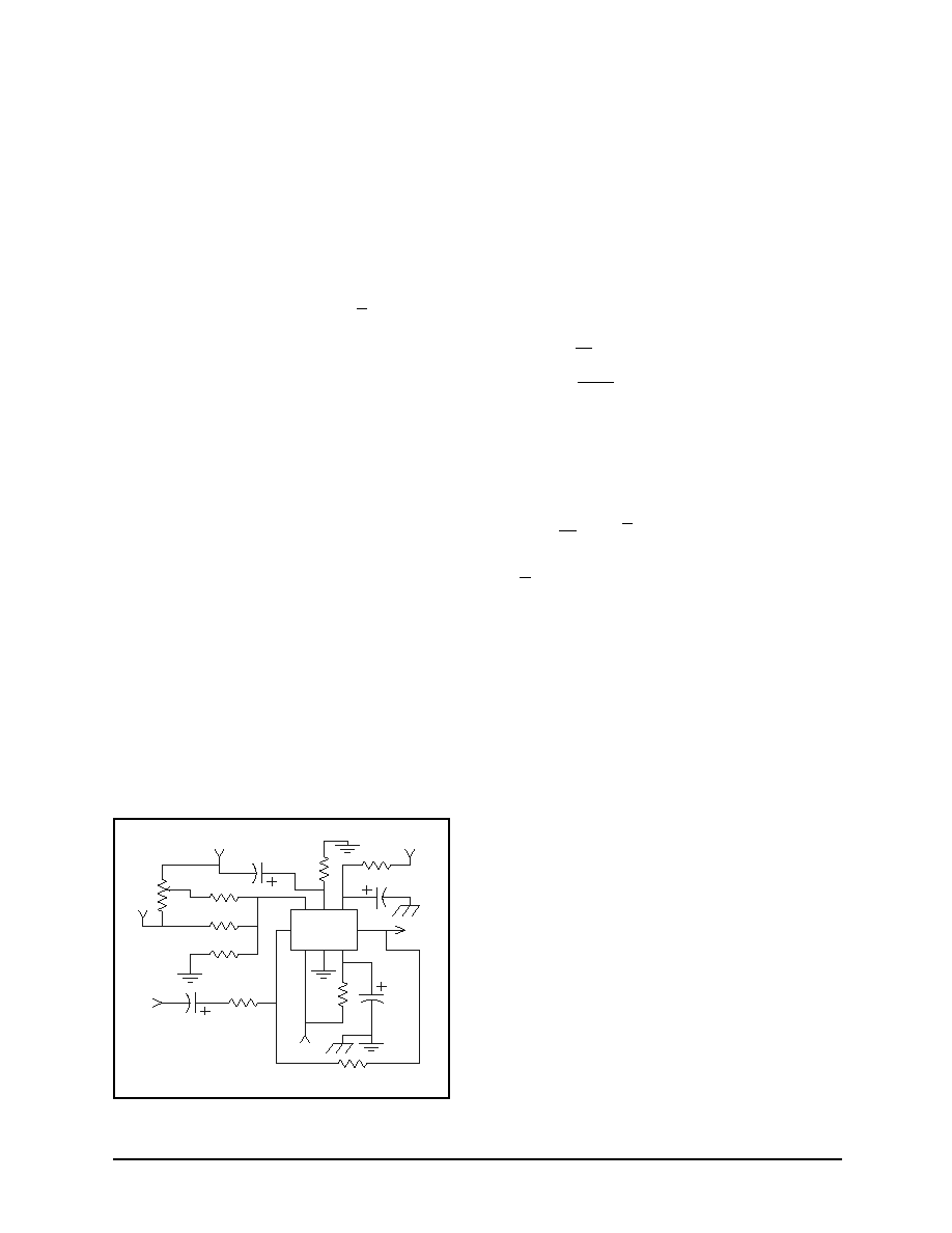
THAT 2252 RMS-Level Detector
V+
V+
OUT
IN
7
2
6
3
8
1
5
4
2252
V+
OUT
CAP
V-
SYM
GND
IBIAS
IN
V-
V-
T
R
T
C
SYM
50k
24k
47k
20
22M
Rf
1k
2M2
560k
1u
Rb
10u
20u
Cin
10u
10k
Rin
Figure 4. Typical Application Circuit (�15V)
given in put fre quency, f
in
. Larger val ues of
re -
duce rip ple at the ex pense of lon ger at tack and re -
lease times. For f
in
>>
1
4 p t
, the rip ple volt age at the
out put is given by: V
R
V
f
T
in
�
4
2
p
t
, where V
R
is the
rms rip ple volt age.
Taking the Square Root
The square root por tion of the Root-Mean Square
is im plied by the con stant of pro por tion al ity for
the out put volt age: it is not com puted ex plic itly.
This is be cause, in the log rep re sen ta tion, tak ing
the square root is equiv a lent to di vi sion by two.
The volt age at pin 6 is pro por tional to the mean of
the square at ap prox i mately 3 mV/dB, and pro por -
tional to the square root of the mean of the square
at ap prox i mately 6 mV/dB.
Out put Buffering and Level Shifting
The volt age at pin 6 is buf fered by OA3, and level
shifted down by the bias volt age V3. Level shift ing
is re quired so that the out put volt age will be zero
when the rms in put cur rent reaches a pre de ter -
mined value, I
in0
. This cur rent is of ten called level
match, and rep re sents the 0 dB ref er ence of the
cir cuit.
The var i ous level shifts through out the 2252 are as
fol lows: V2 rep re sents one di ode drop, so the volt -
age at the emit ter of Q4 is +1V
BE
. The out put of
OA2 is two di ode drops higher than this, or
+3V
BE
. Q6 will sub tract one di ode drop from the
out put of OA2, so the volt age at pin 6 will be
+2V
BE
. Finally, V3 rep re sents two di ode drops,
set ting the volt age at pin 7 to 0 V.
Of course, the ac tual value of all these level shifts
is de pend ent on the cur rents through the tran sis -
tors re spon si ble for each V
BE
. These cur rents, in
turn, are de pend ent on the bias pro gram ming cur -
rent in pin 2 (I
BIAS
) and the tim ing cur rent pulled
from pin 6 (I
T
). This de pend ence may be given as
fol lows:
I
in
I
I
BIAS T
0
2 9
=
.
, where I
in0
is the in put cur rent
caus ing 0 V out put, I
T
is the cur rent in pin 6, and
I
BIAS
is the cur rent in pin 2. The fac tor 2.9 de rives
from the ge om e try of the tran sis tors in volved.
Fig ure 6 plots out put volt age ver sus in put level for
a 2252 in its rec om mended cir cuit con fig u ra tion
(Fig ure 4). In this plot, 0 dBr
43 mV. Fig ure 7
plots out put volt age for sev eral dif fer ent con -
stant-amplitude fre quency sweeps for the same cir -
cuit. The ver ti cal di vi sions are 60 mV apart,
rep re sent ing ap prox i mately 10 dB in cre ments. Full
au dio band width is main tained over a 60 dB dy -
namic range.
Cur rent Pro gramming
All the in ter nal cur rent sources in the 2252 are
slaved to the cur rent in pin 2, I
BIAS
. As men tioned
above, the choice of this cur rent af fects I
in0
. I
BIAS
is nor mally set by a re sis tor from pin 2 to ground
(V
CC
would do also). Note that the volt age at pin 2
is nor mally V
EE
+ 2.1 V, where V
EE
is the neg a tive
sup ply volt age.
Sym me try Ad just ment
The rec ti fier (Q1 through Q3 and OA1) de pends on
the match ing be tween Q1 and Q2 for ac cu rate re -
THAT Corporation; 45 Sumner Street; Milford, Massachusetts 01757-1656; USA
Tel: +1 508 478 9200; Fax: +1 508 478 0990; Web: www.thatcorp.com
600032 Rev 02
Page 5
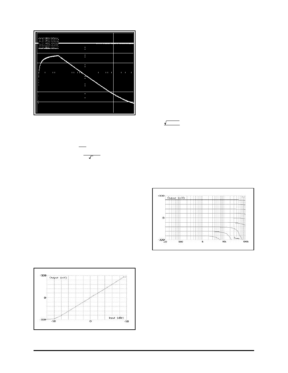
Fig ure 6. 2252 DC Out put Vs. AC In put Level
Fig ure 7. 2252 DC Out put Vs. Fre quency at
Var i ous Levels
Fig ure 5. Tone Burst Re sponse