 | –≠–ª–µ–∫—Ç—Ä–æ–Ω–Ω—ã–π –∫–æ–º–ø–æ–Ω–µ–Ω—Ç: THAT4301A | –°–∫–∞—á–∞—Ç—å:  PDF PDF  ZIP ZIP |

THAT Corporation; 45 Sumner Street; Milford, Massachusetts 01757-1656; USA
Tel: +1 (508) 478-9200; Fax: +1 (508) 478-0990; Web: www.thatcorp.com
T H A T
C o r p o r a t i o n
THAT Analog Engine
Æ
IC Dynamics Processor
THAT 4301, 4301A
FEATURES
∑
High-Performance Voltage
Controlled Amplifier
∑
High-Performance RMS-Level
Detector
∑
Three General-Purpose Opamps
∑
Wide Dynamic Range: >115 dB
∑
Low THD: <0.03%
∑
Low Cost: $4.39 (`000s)
∑
DIP & Surface-Mount Packages
APPLICATIONS
∑
Compressors
∑
Limiters
∑
Gates
∑
Expanders
∑
De-Essers
∑
Duckers
∑
Noise Reduction Systems
∑
Wide-Range Level Meters
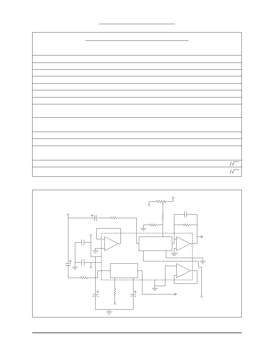
Description
THAT
4301
Dynamics
Processor,
dubbed
"THAT Analog Engine," combines in a single IC
all the active circuitry needed to construct a
wide range of dynamics processors. The 4301
includes
a
high-performance,
exponen-
tially-controlled
VCA,
a
log-responding
RMS-level sensor and three general- purpose
opamps.
The VCA provides two opposing-polarity, volt-
age-sensitive control ports. Dynamic range ex-
ceeds 115 dB, and THD is typically 0.003% at 0
dB gain. In the 4301A, the VCA is selected for
low THD at extremely high levels. The RMS de-
tector provides accurate rms-to-dc conversion
over an 80 dB dynamic range for signals with
crest factors up to 10. One opamp is dedicated
as a current-to-voltage converter for the VCA,
while the other two may be used for the signal
path or control voltage processing.
The combination of exponential VCA gain con-
trol and logarithmic detector response -- "deci-
bel-linear"
response
--
simplifies
the
mathematics of designing the control paths of
dynamics processors. This makes it easy to de-
sign audio compressors, limiters, gates, ex-
panders, de-essers, duckers, noise reduction
systems and the like. The high level of integra-
tion ensures excellent temperature tracking be-
tween
the
VCA
and
the
detector,
while
minimizing the external parts count.
OUT
CT
IT
IN
-
+
-
1
18
11
17
14
13
12
15
16
19
20
2
5
4
9
10
8
6
7
-
OA1
+
VCC
THAT4301
EC-
EC+
IN
OUT
SYM
VCA
OA3
+
OA2
GND VEE
RMS
Figure 1. Block Diagram (pin numbers are for DIP only)

THAT Corporation; 45 Sumner Street; Milford, Massachusetts 01757-1656; USA
Tel: +1 (508) 478-9200; Fax: +1 (508) 478-0990; Web: www.thatcorp.com
Page 2
Rev. 04/10/02
SPECIFICATIONS
1 , 2
Absolute Maximum Ratings (T
A
= 25∞C)
Positive Supply Voltage (V
CC
)
+18 V
Negative Supply Voltage (V
EE
)
-18 V
Supply Current (I
CC
)
20 mA
Power Dissipation (P
D
) (T
A
= 75∞C)
700
mW
Operating Temperature Range (T
OP
)
0 to +70∞C
Storage Temperature Range (T
ST
)
-40 to +125∞C
Overall Electrical Characteristics
Parameter
Symbol
Conditions
Min
Typ
Max
Units
Positive Supply Voltage
V
CC
+7
--
+15
V
Negative Supply Voltage
V
EE
-7
--
-15
V
Positive Supply Current
I
CC
--
12
18
mA
Negative Supply Current
I
EE
--
-12
-18
mA
Thermal Resistance
q
J-C
SO-Package
--
140
--
∞C/W
VCA Electrical Characteristics
3
4301
4301A
Parameter
Symbol
Conditions
Min
Typ
Max
Min
Typ
Max
Units
Input Bias Current
I
B(VCA)
No Signal
--
30
400
--
30
400
pA
Input Offset Voltage
V
OFF(VCA In)
No Signal
--
±4
±15
--
±4
±15
mV
Input Signal Current
I
IN(VCA)
or I
OUT(VCA)
--
175
750
--
175
750
mArms
Gain at 0V Control
G
0
E
C+
= E
C≠
= 0.000V
-0.4
0.0
+0.4
-0.4
0.0
+0.4
dB
Gain-Control Constant
T
A
= 25∞C (T
CHIP
@ 55∞C)
-60 dB < gain < +40dB
E
C+
/Gain (dB)
E
C+
& SYM
6.4
6.5
6.6
6.4
6.5
6.6
mV/dB
E
C-
/Gain (dB)
E
C-
-6.4
-6.5
-6.6
-6.4
-6.5
-6.6
mV/dB
Gain-Control TempCo
DE
C
/
DT
CHIP
Ref T
CHIP
= 27∞C
--
+0.33
--
--
+0.33
--
%/∞C
Gain-Control Linearity
-60 to +40 dB gain
--
0.5
2
--
0.5
2
%
Off Isolation
E
C+
=SYM=-375mV, E
C-
=+375mV 110
115
--
110
115
--
dB
Output Offset Voltage Change
DV
OFF(OUT)
R
out
= 20k
W
0 dB gain
--
1
3
--
1
3
mV
+15 dB gain
--
2
10
--
2
10
mV
+30 dB gain
--
5
25
--
5
25
mV
Gain Cell Idling Current
I
IDLE
--
20
--
--
20
--
mA
Output Noise
e
n(OUT)
20 Hz-20 kHz
R
out
= 20k
W
0 dB gain
--
-96
-94
--
-96
-94
dBV
+15 dB gain
--
-85
-83
--
-85
-83
dBV
Total Harmonic Distortion
THD
V
IN
= 0 dBV, 1 kHz
0 dB gain
--
0.003 0.007
--
0.003 0.007
%
1. All specifications subject to change without notice.
2. Unless otherwise noted, T
A
=25∞C, V
CC
= +15V, V
EE
= -15V; VCA
SYM
adjusted for min THD @ 1 V, 1 kHz, 0 dB gain.
3. Test circuit is the VCA section only from Figure 2.

THAT Corporation; 45 Sumner Street; Milford, Massachusetts 01757-1656; USA
Tel: +1 (508) 478-9200; Fax: +1 (508) 478-0990; Web: www.thatcorp.com
THAT 4301 Dynamics Processor IC
Page 3
SPECIFICATIONS
1 , 2
(Cont'd.)
VCA Electrical Characteristics
3
(Cont'd.)
4301
4301A
Parameter
Symbol
Conditions
Min
Typ
Max
Min
Typ
Max
Units
Total Harmonic Distortion (cont'd.) THD
V
IN
= +10 dBV, 1 kHz
0 dB gain
--
0.03
0.07
--
0.03
0.07
%
≠15 dB gain
--
0.035 0.09
--
0.035 0.09
%
V
OUT
= +10 dBV, 1 kHz
+15 dB gain
--
0.035 0.09
--
0.035 0.09
%
V
IN
= +19.5 dBV, 1 kHz
0 dB gain
--
--
--
--
0.05
0.09
%
Symmetry Control Voltage
V
SYM
minimum THD
-2.5
0
+2.5
-2.5
0
+2.5
mV
RMS Detector Electrical Characteristics
4
Parameter
Symbol
Conditions
Min
Typ
Max
Units
Input Bias Current
I
B (RMS)
No Signal
--
30
400
pA
Input Offset Voltage
V
OFF(RMS In)
No Signal
--
±4
±15
mV
Input Signal Current
I
IN(RMS)
--
175
750
mA
Input Current for 0 V Output
I
in0
I
T
= 7.5
mA
6
8.5
12
mA
Output Scale Factor
E
O
/ 20log(
I
in
/I
in0
)
31.6nA< I
IN
< 1mA
T
A
= 25∞C (T
CHIP
ª55∞C)
6.4
6.5
6.6
mV/dB
Scale Factor Match (RMS to VCA)
-20 dB < VCA Gain < +20 dB
1
mA<I
in (DET)
<100
mA
.985
1
1.015
Output Linearity
f
IN
= 1kHz
1
mA < I
in
< 100
mA
--
0.1
--
dB
100nA <
I
in
< 316
mA
--
0.5
--
dB
31.6nA <
I
in
< 1mA
--
1.5
--
dB
Rectifier Balance
f
IN
= 100 Hz,
t = .001 s
1
mA< I
in
< 100
mA
≠20
--
20
%
Crest Factor
1ms pulse repetition rate
0.2 dB error
--
3.5
--
0.5 dB error
--
5
--
1.0 dB error
--
10
--
Maximum Frequency for 2 dB Additional Error
I
in
≥ 10mA
--
100
--
kHz
I
in
≥ 3mA
--
45
--
kHz
I
in
≥ 300nA
--
7
--
kHz
Timing Current Set Range
I
T
1.5
7.5
15
mA
Voltage at I
T
Pin
I
T
= 7.5
mA
-10
+20
+50
mV
Timing Current Accuracy
I
CT
/I
T
I
T
= 7.5
mA
0.90
1.1
1.30
Filtering Time Constant
t
T
CHIP
= 55
∞C
(
)
0 026
.
C
I
T
T
s
Output Temp. Coefficient
DE
o
/
DT
CHIP
Re: T
CHIP
= 27
∞C
--
0.33
--
%/∞C
Output Current
I
OUT
≠300mV < V
OUT
< +300mV
±90
±100
--
mA
4. Except as noted, test circuit is the RMS-Detector section only from Figure 2.
THAT Corporation; 45 Sumner Street; Milford, Massachusetts 01757-1656; USA
Tel: +1 (508) 478-9200; Fax: +1 (508) 478-0990; Web: www.thatcorp.com
Page 4
Rev. 04/10/02
Specifications
1 , 2
(Cont'd)
Opamp Electrical Characteristics
5
OA1
OA2
OA3
Parameter
Symbol
Conditions
Min
Typ
Max
Min
Typ
Max
Min
Typ
Max
Units
Input Offset Voltage
V
OS
--
±0.5 ±6
--
±0.5
±6
--
±0.5 ±6
mV
Input Bias Current
I
B
--
150
500
--
150
500
--
150
500
nA
Input Offset Current
I
OS
--
15
50
--
15
50
N/A
nA
Input Voltage Range
I
VR
--
±13.5 --
--
±13.5 --
N/A
V
Common Mode Rej. Ratio
CMRR
R
S
<10k
--
100
--
--
100
--
N/A
Power Supply Rej. Ratio
PSRR
VS=
±7V to ±15V
--
100
--
--
100
--
--
100
--
Gain Bandwidth Product
GBW
(@50kHz)
--
5
--
--
5
--
--
5
--
MHz
Open Loop Gain
A
VO
R
L
=10k
--
115
--
--
110
--
--
125
--
R
L
=2k
N/A
N/A
--
120
--
Output Voltage Swing
V
O
@R
L
=5k
W
--
±13
--
--
±13
--
--
±14
--
V
V
O
@R
L
=2k
W
N/A
N/A
--
--
±13
--
V
Short Circuit Output Current
--
4
--
--
4
--
--
12
--
mA
Slew Rate
SR
--
2
--
--
2
--
--
2
--
V/
ms
Total Harmonic Distortion
THD
1kHz, A
V
=1, R
L
=10k
W -- 0.0007 0.003 -- 0.0007 0.003 -- 0.0007 0.003 %
1kHz, A
V
=≠1, R
L
= 2k
W
N/A
N/A
-- 0.0007 0.003
%
Input Noise Voltage Density
e
n
f
O
=1kHz
--
6.5
10
--
7.5
12
--
7.5
12
nV Hz
Input Noise Current Density
i
n
f
O
=1kHz
--
0.3
--
--
0.3
--
--
0.3
--
pA Hz
50K
R5
47uF
C1
10uF
C4
22uF
C6
300K
R4
51
R3
1%
R1
1%
R2
47pF
C2
1%
10K0
R6
47uF
C3
1%
2M00
R7
100n
C7
100n
C8
Ct
OA2
OA1
VEE
VCC
GND
-
+
VCA
-
-
+
VCA SYM
IN
SIGNAL
Ec-
OUT
SIGNAL
OUT
RMS
+15V
+15V
-15V
-15V
-15V
20K0
20K0
THAT4301
IN
RMS
It
SYM
OUT
IN
EC-
EC+
OA3
OUT
+
Figure 2. VCA and RMS detector test circuit
5. Test circuit for opamps is a unity-gain follower configuration, with load resistor R
L
as specified.
THAT Corporation; 45 Sumner Street; Milford, Massachusetts 01757-1656; USA
Tel: +1 (508) 478-9200; Fax: +1 (508) 478-0990; Web: www.thatcorp.com
THAT 4301 Dynamics Processor IC
Page 5
Pin Name
DIP P in
SO Pin
RMS In
1
3
I
T
(I
Time
)
2
4
No Connection
3
5
RMS Out
4
6
C
T
(C
Time
)
5
7
OA2 -In
6
9
OA2 Out
7
10
OA2 +In
8
11
GND
9
12
VEE
10
13
VCC
11
18
OA3 Out
12
19
VCA Out
13
20
SYM
14
22
E
C+
15
23
Pin Name
DIP P in
SO Pin
E
C-
16
24
VCA In
17
25
OA1 Out
18
26
OA1 -In
19
27
OA1 +In
20
28
No Connection
1
No Connection
2
No Connection
8
No Connection
14
No Connection
15
No Connection
16
No Connection
17
No Connection
21
No Connection
29
No Connection
30
Table 1. Pin Connections
1
B
A
C
D
P
J
I
K
N
L
M
O
H
F
G
E
ITEM
A
B
C
D
E
F
G
H
I
J
K
L
M
N
O
P
MILLIMETERS
INCHES
24.8 Max.
0.98 Max
24.2 +/-0.2
0.95 +/-0.008
6.4 +/-0.2
0.25 +/-0.008
7.62 +/-0.25
0.30 +/-0.01
2.54 +/-0.15
0.10 +/-0.006
0.46 +0.15 -0.1
0.02 +0.006 -0.004
1.0 +/-0.15
0.04 +/-0.006
1.5 Typ.
0.06 Typ.
0.98 Typ.
0.04 Typ.
1.5
0.06
1.75
0.07
3.25 +/-0.15
0.13 +/-0.006
4.7 Max.
0.19 Max.
0.51 Min.
0.02 Min.
2.8 Min.
0.11 Min.
0.25 +0.15 -0.05
0.01 +0.006 -0.002
0-15
Figure 3. Plastic dual in-line package outline
B
C
J
G
I
H
E
D
A
1
+ 0.1 - 0.05
Typ.
+/- 0.2
+ 0.1 - 0.05
+/- 0.4
+/- 0.3
J
0.2
I
0.8
H
0.15
G
2.3
F
0.85 MAX.
E
1.0
D
0.4
C
10.3
B
7.5
15.4
A
MILLIMETERS
ITEM
F
+/- 0.1
+/- 0.15
INCHES
0.60 +/- 0.012
0.29 +/- 0.008
0.41 +/- 0.016
0.002 +0.004 -0.002
0.039 Typ.
0.033 Max.
0.09 +/- 0.006
0.006 +/- 0.004
0.031
0.008 +0.004 -0.002
0-10
Figure 4. Plastic surface-mount package outline
Ordering Information
Plastic DIP
4301P
4301PA
Plastic Surface Mount
4301S
Inquire