 | –≠–ª–µ–∫—Ç—Ä–æ–Ω–Ω—ã–π –∫–æ–º–ø–æ–Ω–µ–Ω—Ç: THAT4305 | –°–∫–∞—á–∞—Ç—å:  PDF PDF  ZIP ZIP |
THAT Corporation; 45 Sumner Street; Milford, Massachusetts 01757-1656; USA
Tel: +1 508 478 9200; Fax: +1 508 478 0990; Web: www.thatcorp.com
Document 600067 Rev 00
T H A T
C o r p o r a t i o n
Pre-trimmed Analog Engine
Æ
IC
THAT
4305
FEATURES
∑
Pre-trimmed BlackmerTM VCA &
RMS-level detector
∑
Wide supply voltage range:
±4.5V ~±16V
∑
Low supply current:
3.5 mA typ. (±15V)
∑
Wide dynamic range:
117 dB (VCA)
60 dB (RMS-level detector)
APPLICATIONS
∑
Compressors & Limiters
∑
Gates & Expanders
∑
AGCs
∑
Line-operated dynamics processors
∑
De-Essers
∑
Duckers
∑
Mixers
∑
Level indicators
∑
Companding noise reduction systems
Description
The THAT4305 is a single-chip Analog En-
gine optimized for low-cost applications. It incor-
porates a high-performance Blackmer voltage-
controlled amplifier (VCA) and log-responding
RMS-level sensor. The VCA and RMS detector
are pre-trimmed at wafer stage to deliver low dis-
tortion without further adjustment.
Available only in a small (QSOP) surface-
mount package, the 4305 is aimed at line-oper-
ated audio applications such as compressor/lim-
iters, gates, and other dynamic processors. The
part normally operates from a split supply volt-
age up to ±16Vdc, drawing only 3.5mA at ±15V.
This IC also works at supply voltages as low as
±4.5V, making it useful in some battery-operated
products as well.
The 4305 was developed specifically for use
in low-cost dynamics processors, drawing from
THAT's long history and experience with such
designs. Both VCA control ports and the detec-
tor input and output are available for the de-
signer to connect as s/he sees fit. As a result, the
part is extremely flexible and can be configured
for a wide range of applications including single-
and multi-band companders, digital overload
protectors, voltage-controlled faders, level indi-
cators, etc.
What really sets the 4305 apart from other
manufacturers' offerings is the transparent sound
of its Blackmer VCA, coupled with its accurate
true-RMS level detector. This makes the IC useful
in a wide range of analog audio products.
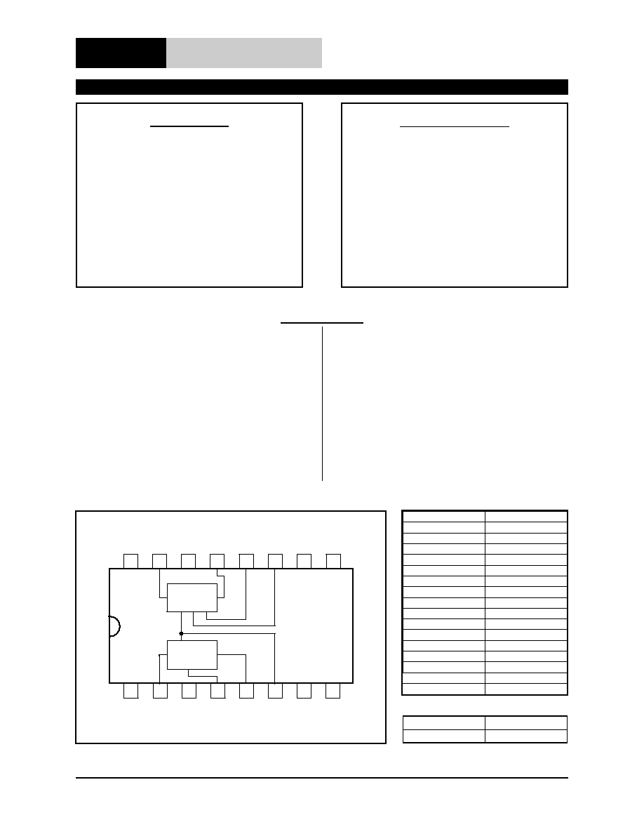
15
2
14
3
13
4
12
5
11
6
10
7
9
8
EC-
EC+
IN
OUT
VCA
IN
CT
OUT
RMS
16
1
VCA
IN
RMS
IN
VCA
OUT
CT
NC
NC
NC
NC
EC-
RMS
OUT
EC+
GND
NC
NC
VCC
VEE
Figure 1. THAT4305 equivalent block diagram
Pin Name
Pin Number
No Connection
1
RMS IN
2
No Connection
3
C
TIME
4
RMS OUT
5
GND
6
NC
7
Vee
8
V
CC
9
No Connection
10
EC+
11
EC-
12
VCA OUT
13
No Connection
14
VCA IN
15
No Connection
16
Table 1. THAT 4305 pin assignments
Package
Order Number
16 pin QSOP
4305Q16-U
Table 2. Ordering Information

THAT Corporation; 45 Sumner Street; Milford, Massachusetts 01757-1656; USA
Tel: +1 508 478 9200; Fax: +1 508 478 0990; Web: www.thatcorp.com
Page 2
THAT4305 Pre-trimmed Analog Engine
Operating Temperature Range (T
OP
)
-40 to +85 ∫C
Junction Temperature (T
J
)
-40 to +125 ∫C
Power Dissipation (P
D
) at T
A
=85 ∫C
400mW
Supply Voltages (V
CC
, V
EE
)
±
18V
VCA Control Voltage
±0.6 V
Storage Temperature Range (T
ST
)
-40 to +125 ∫C
Absolute Maximum Ratings
1
Power Supply
Positive Supply Voltage
V
CC
Referenced to GND
+4.5
-
+16
V
Negative Supply Voltage
V
EE
Referenced to GND
-4.5
-
-16
V
Supply Current
No Signal
I
CC
V
CC
=+15V, V
EE
= -15V
3.5
5
mA
I
EE
V
CC
=+15V, V
EE
= -15V
-3.5
-5
mA
I
CC
V
CC
=+5V, V
EE
= -5V
2
mA
I
EE
V
CC
=+5V, V
EE
= -5V
-2
mA
Voltage Controlled Amplifier (VCA)
Max. I/O Signal Current
i
IN(VCA)
+ i
OUT(VCA)
±1.8
mA
peak
VCA Gain Range
-60
+60
dB
Gain at 0V Control
G
0
E
C+
= E
C-
= 0V
-1.0
0
+1.0
dB
Gain-Control Constant
E
C+
/Gain (dB)
-60 dB < gain < +60 dB
-
6.2
-
mV/dB
Gain-Control Tempco
E
C
/
T
CHIP
Ref T
CHIP
=27∫C
-
+0.33
-
%/∫C
Output Offset Voltage Change
3
V
OFF(OUT)
R
OUT
= 20 k
0 dB gain
-
1
15
mV
+15 dB gain
-
3
30
mV
+30 dB gain
-
10
50
mV
Output Noise
e
N(OUT)
0 dB gain
22Hz~22kHz, R
IN
=R
OUT
=20 k
-
-97.5
-95
dBV
Total Harmonic Distortion
THD
V
IN
= -5dBV, 1kHz, E
C+
= E
C-
= 0V
0.07
0.15
%
RMS level detector
Output Voltage at Reference i
IN
e
O(0)
i
IN
= 7.5
µ
A RMS
-9
0
+9
mV
Output Error at Input Extremes
e
O(RMS)error
i
IN
= 200 nA RMS
±1
±3
dB
i
IN
= 200
µ
A RMS
±1
±3
dB
Scale Factor Match to VCA
-20 dB < VCA gain < +20 dB
1
µ
a< i
IN(RMS)
< 100
µ
A
.95
1
1.05
-
Electrical Characteristics
2
Parameter
Symbol
Conditions
Min
Typ
Max
Units
SPECIFICATIONS
1. If the devices are subjected to stress above the Absolute Maximum Ratings, permanent damage may result. Sustained operation at
or near the Absolute Maximum Ratings conditions is not recommended. In particular, like all semiconductor devices, device reliabil-
ity declines as operating temperature increases.
2. Unless otherwise noted, T
A
=25∫C, V
CC
=+15V, V
EE
= -15V.
3. Reference is to output offset with -60dB VCA gain.

THAT Corporation; 45 Sumner Street; Milford, Massachusetts 01757-1656; USA
Tel: +1 508 478 9200; Fax: +1 508 478 0990; Web: www.thatcorp.com
Document 600067 Rev 00
Page 3
Theory of Operation
The THAT 4305 Dynamics Processor combines
THAT Corporation's proven exponentially controlled
BlackmerTM Voltage-Controlled Amplifier (VCA) and
log-responding RMS-Level Detector building blocks
in a small package optimized for low cost designs.
The part is fabricated using a proprietary, fully com-
plementary, dielectric-isolation process. This pro-
cess produces very high-quality bipolar transistors
(both NPNs and PNPs) with unusually low collector-
substrate capacitances. The 4305 takes advantage of
these devices to deliver wide bandwidth and excel-
lent audio performance while consuming very low
Rectifier Balance
±7.5
µ
A DC
IN
±1
±3
dB
Timing Current
I
T
-
7.5
-
µ
A
Filtering Time Constant
3467 X C
TIME
s
Output Tempco
E
O
/
T
CHIP
Ref T
CHIP
= 27 ∫C
-
+0.33
-
%/∫C
Load Resistance
R
L
-250mV < V
OUTRMS
< +250mV
2
k
Capacitive Load
C
L
150
pf
Electrical Characteristics (con't)
2
Parameter
Symbol
Conditions
Min
Typ
Max
Units
Surface Mount Package
Type
See Fig. 23 for dimensions
16 Pin QSOP
Thermal Resistance
JC
SO package in ambient
105
∫C/W
Thermal Resistance
JA
SO package soldered to board
40
∫C/W
Environmental Regulation Compliance
Complies with RoHS requirements
Soldering Reflow Profile
JEDEC JESD22-A113-D (250 ∫C)
Package Characteristics
Parameter
Symbol
Conditions
Min
Typ
Max
Units
R1
5k1
C1
10u
R2
20k
C3
22p NPO
R3
20k
C2
10u
10u
C5
100p
R4
6k8
VCA Out
13
VCA In
15
U1A
THAT4305
RMS In
2
RMS Out
5
U1B
THAT4305
+15V
-15V
VCA Out
VCA In
RMS In
RMS Out
Control Voltage
U2
R5
2k
Vcc
Gnd
Vee
Ec-
Ec+
9
11
6
8
12
4
CT
C
TIME
C4
10u
+15V
Figure 2. Simplified application circuit

THAT Corporation; 45 Sumner Street; Milford, Massachusetts 01757-1656; USA
Tel: +1 508 478 9200; Fax: +1 508 478 0990; Web: www.thatcorp.com
Page 4
THAT4305 Pre-trimmed Analog Engine
current and operating over a wide range of power
supply voltages.
For details of the theory of operation of the VCA
and RMS Detector, we refer the interested reader to
THAT Corporation's data sheets on the 2180-Series
VCAs and the 2252 RMS Level Detector. Theory of
the interconnection of exponentially controlled VCAs
and log-responding level detectors is covered in
THAT Corporation's application note AN101A, The
Mathematics of Log-Based Dynamic Processors.
The VCA - in Brief
The VCA in the 4305 is based on THAT Corpora-
tion's highly successful complementary log-antilog
gain cell topology (the BlackmerTM VCA) as used in
THAT 2180-Series IC VCAs. VCA symmetry is
trimmed during wafer probe for minimum distor-
tion. No external adjustment is allowed.
Input signals are currents in the VCA's VCA
IN
pin
(pin 15). This pin is a virtual ground with a small dc
offset, so in normal operation an input voltage is
converted to input current via an appropriately sized
resistor (R3 in Figure 2). Because the dc current as-
sociated with dc offsets present at the input pin plus
any dc offset in the preceding stages will be modu-
lated by gain changes (thereby becoming audible as
thumps), the input pin is normally ac-coupled. This
blocks such offset currents and reduces dc offset
variation with gain.
The VCA output signal, VCA
OUT
(pin 13), is also
a current, inverted with respect to the input current.
In normal operation, the output current is converted
to a voltage via an external op-amp, where the cur-
rent-to-voltage conversion ratio is determined by the
feedback resistor connected between the op-amp's
output and its inverting input (R2 in Figure 2). The
resulting signal path through the VCA plus op-amp
is noninverting.
The VCA gain is controlled by the voltage applied
between E
C+
(pin 11) and E
C-
(pin 12). Note that any
unused control port should be connected to ground
(as E
C+
is in Figure 2). The gain (in decibels) is pro-
portional to (E
C+
- E
C-
). The constant of proportion-
ality is 6.2 mV/dB for the voltage at E
C+
(relative to
E
C-
). Note that neither E
C+
or E
C-
should be driven
more than ±0.6 V away from ground.
The VCA's noise performance varies with gain in
a predictable way, but due to the way internal bias
currents vary with gain, noise at the output is not
strictly the product of a static input noise times the
voltage gain commanded. At large attenuation, the
noise floor is usually limited by the input noise of
the output op-amp and its feedback resistor. At 0 dB
gain, the noise floor of ~ -97.5 dBV is the result of
the VCA's output noise current, converted to a volt-
age by the typical 20k I-V converter resistor (R2 in
Figure 2). In the vicinity of 0 dB gain, the noise in-
creases more slowly than the gain: approximately
5 dB noise increase for every 10 dB gain increase.
Finally, as gain approaches 30 dB, output noise be-
gins to increase directly with gain.
While the 4305's VCA circuitry is very similar to
that of the THAT 2180 Series VCAs, there are sev-
eral important differences, as follows.
1. Supply current for the 4305 VCA depends on
the supply voltage. At ±5 V, approximately 800 uA is
available for the sum of input and output signal cur-
rents. This increases to about 1.8 mA at ±15 V.
(Compare this to ~1.8 mA for a 2180 Series VCA
when biased as recommended.)
2. The SYM control port (similar to that on the
2180 VCA) is not brought out to an external pin; it is
driven from an internally trimmed current genera-
tor.
3. The control-voltage constant is approximately
6.2 mV/dB, due primarily to the higher internal op-
erating temperature of the 4305 compared to that of
the 2180 Series.
The RMS Detector - in Brief
The 4305's detector computes RMS level by rec-
tifying input current signals, converting the rectified
current to a logarithmic voltage, and applying that
voltage to a log-domain filter. The output signal is a
dc voltage proportional to the decibel-level of the
RMS value of the input signal current. Some ac com-
ponent (at twice the input frequency plus higher-
order even harmonics) remains superimposed on
the dc output. The ac signal is attenuated by a log
domain filter, which constitutes a single-pole rolloff
with cutoff determined by an external capacitor (C4
in Figure 2).

The rectifier is balanced to within ±3 dB, so a
small amount of fundamental (and higher odd-order
harmonics) ripple can be present at the detector out-
put. By design, this ripple contributes less total rip-
ple than the even-order products that are naturally
and inevitably present at the output of a perfectly
balanced detector.
As in the VCA, input signals are currents to the
RMS
IN
pin (pin 2). This input is a virtual ground, so
a resistor (R1 in Figure 2) is normally used to con-
vert input voltages to the desired current. The level
detector is capable of accurately resolving signals
well below 10 mV (with a 5 k
input resistor). How-
ever, if the detector is to accurately track such
low-level signals, ac coupling (C1 in Figure 2) is re-
quired to prevent dc offsets from causing a dc cur-
rent to flow in the detector's input, which would
obscure low-level ac signal currents.
The log-domain filter cutoff frequency is usually
placed well below the frequency range of interest.
For an audio-band detector, a typical value would be
5 Hz, or a 32 ms time constant (
). The filter's time
constant is determined by an external timing capaci-
tor (C
TIME
) attached to the C
T
pin (pin 4), and an in-
ternal current source (I
T
) connected to C
T
. The
current source is internally fixed at 7.5 µA. The re-
sulting time constant in seconds is approximately
equal to 3467 times the value of the timing capacitor
in Farads. Note that, as a result of the mathematics
of RMS detection, the attack and release time con-
stants are fixed in their relationship to each other.
The RMS detector is capable of driving large
spikes of current into C
TIME
, particularly when the
audio signal input to the RMS detector increases
suddenly. This current is drawn from V
CC
(pin 9),
fed through C
TIME
at pin 4, and returns to the power
supply through the ground end of C
TIME
. If not han-
dled properly through layout and bypassing, these
currents can mix with the audio in the circuit's
ground structure with unpredictable and undesir-
able results. As noted in the Applications section,
local bypassing from the V
CC
pin to the ground end
of C
TIME
is strongly recommended in order to keep
these currents out of the ground structure of the cir-
cuit (see C4 in Figure 2.)
The dc output of the detector is scaled with the
same constant of proportionality as the VCA gain
control: 6.2 mV/dB. The detector's 0 dB reference
(i
in0
, the input current which causes the detector's
output to equal 0V), is trimmed during wafer probe
to equal approximately 7.5 µA. The RMS detector
output stage is capable of sinking or sourcing
125 µA. It is also capable of driving up to 150 pF of
capacitance.
Frequency response of the detector extends
across the audio band for a wide range of input sig-
nal levels. Note, however, that it does fall off at high
frequencies at low signal levels like THAT's other
RMS detectors.
Differences
between
the
4305's
RMS
level
detector circuitry and that of the THAT 2252 RMS
detector include the following.
1. The rectifier in the 4305 RMS Detector is in-
ternally balanced by design, and cannot be balanced
via an external control. The 4305 will typically bal-
ance positive and negative halves of the input signal
within 10 %, but in extreme cases the mismatch may
reach +40 % or -30 % (±3 dB). However, even such
extreme-seeming mismatches will not significantly
increase ripple-induced distortion in dynamics pro-
cessors over that caused by balanced signal ripple
alone.
2. The time constant of the 4305's RMS detector
is determined by the combination of an external ca-
pacitor C
TIME
and an internal current source. The in-
ternal current source is set to about 7.5 µA. A
resistor is not normally connected directly to the C
T
pin on the 4305.
3. The 0 dB reference point, or level match, is
also set to approximately 7.5 µA. However, as in the
2252, the level match will be affected by any addi-
tional currents drawn from the C
T
pin.
Compressor (or Limiter) Configurations
The 4305 provides the two essential building
blocks required for a wide variety of dynamics pro-
cessing applications.
The part may be configured
into practically any type of dynamics processor sys-
tem.
Perhaps the most common application for the
4305 is as a compressor or limiter. These circuits
are intended to reduce gain above some determined
signal level in order to prevent subsequent stages
from being overloaded by too high a signal.
Com-
pressors generally have low to moderate compres-
THAT Corporation; 45 Sumner Street; Milford, Massachusetts 01757-1656; USA
Tel: +1 508 478 9200; Fax: +1 508 478 0990; Web: www.thatcorp.com
Document 600067 Rev 00
Page 5

THAT Corporation; 45 Sumner Street; Milford, Massachusetts 01757-1656; USA
Tel: +1 508 478 9200; Fax: +1 508 478 0990; Web: www.thatcorp.com
Page 6
THAT4305 Pre-trimmed Analog Engine
sion ratios, while limiters have high ratios. In such
applications, the signal path has static gain so long
as the input signal remains below some threshold,
but gain is reduced when the signal rises above the
threshold. Compression ratio is defined as the num-
ber of dB the input signal increases for a 1 dB in-
crease in output signal.
Feedforward Topologies
To make a compressor or limiter with a 4305,
typically, the input signal is applied to both the VCA
and the RMS detector. The RMS output signal is fed
forward to the VCA's negative control port (E
C-
) via a
dc-coupled op-amp based stage. This stage has gain
above some dc level (the threshold), and no trans-
mission below that level. This path, called the
"sidechain," -- from detector output to VCA control
port -- determines the compression behavior of the
circuit. As signal level rises, the dc voltage at the
RMS' output rises.
Once the dc level exceeds the
threshold, the rms output signal is transmitted
through the sidechain and presented to the VCA con-
trol port, lowering the gain to signals passing
through the VCA. As a result, the output signal level
is reduced, or compressed, relative to rising input
signal levels.
Varying the threshold setting of the sidechain will
vary the point at which compression begins. Varying
the gain between the RMS output and the VCA con-
trol input varies the compression ratio.
Feedforward compressor topologies are espe-
cially versatile because they cannot become unstable
due to oscillation in the control loop. Unity gain in
the sidechain produces infinite compression (where
the output remains constant regardless of increases
in the input signal). With feedforward, negative com-
pression ratios are easily achievable. (Negative com-
pression occurs when the output signal decreases
as the input signal increases.) This approximates the
effect of playing music backwards, since the attack
is suppressed and the release is increased in vol-
ume.
Many other variations of the feedforward concept
are possible. These include implementing more than
one threshold, different ratios, additional time con-
stants, ac-coupling of some (or all) of the detector
output signal, and many more. See AN101A, The
Mathematics of Log-Based Dynamic Processors, for
more details of how the sidechain gain determines
compression ratios.
Feedback Topologies
An alternative configuration for compressor/lim-
iter design is to feed the output signal into the RMS
detector. The RMS output is fed back (dc coupled)
to the VCA's negative control port to reduce signal
levels.
Similarly as with a feedforward designs, a
threshold in the sidechain serves to stop the com-
pression action at low signal levels.
The feedback topology behaves somewhat differ-
ently from feedforward. First, reaching infinite com-
pression requires infinite gain in the feedback loop
from RMS output to VCA control port. Of course, in-
finite gain is impossible, so practical feedback com-
pressors are usually limited to ratios no greater than
20 or so. Additionally, the gain in the feedback loop
alters the effective time constant of the detector,
shortening the attack as the ratio becomes higher.
This may or may not be appropriate, depending on
the desired effect.
Expander (Gate) Configurations
By changing the sign of the sidechain in a
feedforward compressor, it is possible to arrange
signal gain to decrease along with signal level, thus
producing an expander.
This is typically applied
below a threshold (so, the threshold detector's po-
larity is reversed from that of a compressor) to re-
duce noise or crosstalk during pauses in program
material.
This technique has long been used for
"cleaning up" individual drum tracks to reduce re-
verberation, interference from microphones picking
up adjacent drum sounds, and alter the attack/decay
characteristic of individual drum sounds.
Practical gates usually require very fast attack
times, and carefully programmable release times. In
a 4305, this is best accomplished by using the RMS
detector as a log rectifier with very short time con-
stants, and following the detector output with a
time-constant stage that applies the desired attack
and release behavior. This alters the 4305 detector's
natural response characteristics to peak, rather than
rms, time constants. We intend to produce an appli-
cation note showing examples of these circuits. Un-
til that is available, see DN 100, which shows a noise
gate application using THAT's 4301 Analog Engine.

Noise Reduction (Compander) Configurations
An additional application of the 4305 is for
noise reduction systems. In these applications, one
Analog Engine is configured for use as a compressor
to condition audio signals before feeding them into a
noisy channel. A second Analog Engine, configured
as an expander, is located at the receiver end of the
noisy channel. Most commonly, the compression/ex-
pansion ratio is modest (e.g. 2:1:2) and is linearly
applied across the entire signal dynamic range.
During low-level audio passages, the compressor
increases signal levels, bringing them up above the
noise floor of the channel. At the receiving end, the
expander reduces the signal back to its original
level, in the process attenuating channel noise.
During high-level audio passages, the compres-
sor decreases signal levels, reducing them to fit
within the headroom limits of the channel. The ex-
pander increases the signal back to its original level.
While the channel noise may be increased by this ac-
tion, in a well-designed compander, at such times
the noise floor will be masked by the high-level sig-
nal.
The 4305 facilitates the design of a wide variety
of companding noise reduction systems. The RMS
detector responds accurately over a wide range of
levels; the VCA responds accurately to a wide range
of gain commands; and all the detector and VCA in-
puts, outputs, and control ports are independently
accessible and fully configurable. All these features
mean that the 4305 will support a wide range of
compander designs, including simple 2:1 wide range
(level-independent) systems, level-dependent sys-
tems with thresholds and varying compression
slopes, systems including noise gating and/or limit-
ing,
and
systems
with
varying
degrees
of
pre-emphasis and filtering in both the signal and de-
tector paths. Furthermore, much of this can be ac-
complished by extensively conditioning the control
voltage sidechain rather than the audio signal itself.
The audio signal can pass through as little as one
VCA and one opamp, and still support multiple ra-
tios, thresholds, and time constants.
Note that the 4305 is fully compatible with other
Analog Engines from THAT Corporation. All our An-
alog Engines feature log-responding true-RMS level
detectors and exponentially controlled Blackmer
VCAs.
It is possible to compress (encode) signals
using the low-voltage, low-power 4315 or 4320 in a
handheld, battery-operated device such as a wireless
microphone or instrument belt pack, and expand
(decode) that signal using the 4305 in a rack-mount,
line-operated receiver.
The Mathematics of Log-Based Dynamics
Processors
At first, the logarithmic output of the RMS detec-
tor and the exponential control ports of the VCA can
be intimidating for designers unfamiliar with THAT
Corporation's offerings.
However, in fact, these
characteristics make developing audio processors
easy once a designer understands the concepts in-
volved. As noted earlier, AN101A: The Mathematics
of Log-Based Dynamics Processors, discusses these
concepts in some detail.
The following discussion
draws heavily from that application note.
The Feedforward Compressor
Figure 3 shows a conceptual diagram of a very
simple feedforward compressor.
Using the "log
math" principles explained in AN101A, we can state
that
Out
In
G
dB
dB
dB
=
+
, and that
G
k In
dB
dB
= -
.
Note that the sign of k makes this a compressor
in which gain G
dB
decreases as input signal level
In
dB
increases. Combining these equations,
Out
In
k In
In
k
dB
dB
dB
=
-
=
-
(
)
1
.
Rearranging yields
In
Out
k
dB
dB
C R
=
=
-
1
1
(
)
. .
This is the compression ratio.
THAT Corporation; 45 Sumner Street; Milford, Massachusetts 01757-1656; USA
Tel: +1 508 478 9200; Fax: +1 508 478 0990; Web: www.thatcorp.com
Document 600067 Rev 00
Page 7
In
In
dB
G
-k
Out
RMS
dB
dB
dB
Figure 3. Simplified feedforward compressor,
conceptual diagram.

THAT Corporation; 45 Sumner Street; Milford, Massachusetts 01757-1656; USA
Tel: +1 508 478 9200; Fax: +1 508 478 0990; Web: www.thatcorp.com
By inspection we can see that if k equals zero,
the compression ratio will be 1:1, and if k equals 1,
the compression ratio will be infinity:1.
Thus, we
can make a feedforward compressor/limiter by hav-
ing the gain of the sidechain vary from zero to one.
Note that if k>1, the compression ratio becomes
negative. Negative compression results with 1<k<2.
The Feedback Compressor
We can use the same approach for a feedback
compressor. Figure 4 shows a simplified theoretical
model of a feedback compressor. By inspection,
Out
In
G
dB
dB
dB
=
+
, and
G
k Out
dB
dB
= -
. Therefore,
Out
In
k Out
dB
dB
dB
=
-
, and
Out
k Out
In
dB
dB
dB
+
=
. As such,
In
Out
dB
dB
k
C R
= + =
1
. . .
In this case, as mentioned earlier, infinite com-
pression requires infinite sidechain gain.
Fortu-
nately, compression ratios of between 10 and 20
limit effectively enough that infinite gain is not re-
quired.
Log-Based Expanders
Similarly, for the feedforward expander shown in
Figure 5, we can state that
Out
In
G
dB
dB
dB
=
+
, and that
G
k In
dB
dB
=
.
Note that the sign of k makes this an expander in
which gain G
dB
decreases as input signal level In
dB
decreases. Combining these equations:
Out
In
k In
dB
dB
dB
=
+
, and
Out
k In
dB
dB
= +
(
)
1
.
Rearranging yields
Out
In
dB
dB
k
E R
= + =
1
. .
This is the expansion ratio.
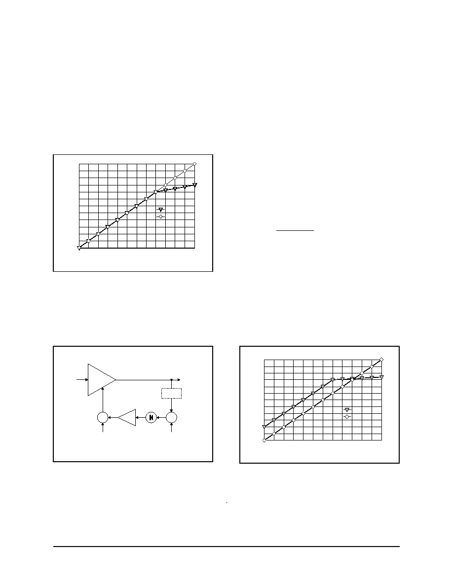
Adjusting the Level Match Point
In the equations so far, we have made the im-
plicit assumption that the decibel reference level ev-
erywhere is that of the rms-level detector.
This
assumption simplifies the math, but it may not cor-
respond to real-world reference levels such as 1V
rms (0 dBV) or 0.775V rms (0 dBu). Additionally, it
is possible to offset the VCA's inherent behavior of
producing unity (0 dB) current gain at 0 mV control
voltage (E
C+
-E
C-
) by selecting asymmetrical volt-
age-to-current and current-to-voltage converting re-
sistors (R3 and R2, respectively, in Figure 2).
Figure 6 allows for a VCA voltage gain offset of
A
dB
, as well as an offset (LM
dB
) to vary the "level
match" point of the RMS detector. Using similar "log
math" from AN101A, we can state for Figure 6:
Out
In
G
A
dB
dB
dB
dB
=
+
+
, where G
dB
is the
VCA's control port gain in dB, and A
dB
is any static
gain or attenuation (in dB) applied to the signal.
We can also state that:
G
k Out
L M
dB
dB
dB
= -
-
(
.
.
) , where L.M. is a vary-
ing dc voltage intended to change the system's zero
dB reference point (often referred to as level match
Page 8
THAT4305 Pre-trimmed Low-power Analog Engine
In
dB
RMS
G
k
Out
In
dB
dB
dB
Figure 5. Simplified feedforward expander,
conceptual diagram
Out
dB
RMS
G
-k
Out
In
dB
dB
dB
Figure 4. Simplified feedback compressor,
conceptual diagram.

THAT Corporation; 45 Sumner Street; Milford, Massachusetts 01757-1656; USA
Tel: +1 508 478 9200; Fax: +1 508 478 0990; Web: www.thatcorp.com
Document 600067 Rev 00
Page 9
point) from that of the detector, and k is the gain of
the sidechain.
Substituting the second equation into the first,
Out
In
k L M
Out
A
dB
dB
dB
dB
dB
=
+
-
+
( .
.
)
, or
Out
In
k L M
k Out
A
dB
dB
dB
dB
dB
=
+ ◊
- ◊
+
.
.
, or
Out
dB
In
k L M
A
k
dB
dB
dB
=
+ ◊
+
+
. .
(
)
1
.
Similarly, for the expander shown in Figure 7, we
can state that:
Out
In
A
G
dB
dB
dB
dB
=
-
+
G
k In
L M
dB
dB
dB
=
-
(
.
.
) . Thus:
Out
k In
k L M
A
dB
dB
dB
dB
= +
- ◊
-
(
)
.
.
1
In both Figures 6 and 7, we show two ways to ad-
just the point at which input and output levels of the
compressor or expander become equal. These are
a) adjusting the 0 dB reference voltage level of the
RMS detector by setting its voltage-to current con-
verting resistor (R1 in Figure 2), and b) varying the
static signal-path gain offset (A
dB
). For the 4305, the
best practice is to achieve level match via a combina-
tion of setting the RMS detector's voltage-to-current
conversion, and offsetting the signal-path gain. Sig-
nal-path gain can be offset by altering the values of
the VCA's voltage-to-current and current-to-voltage
resistors. Both of these approaches have the advan-
tage of being temperature-independent.
Figure 8 shows the behavior of the compressor
of Figure 6 with varying sidechain gain k for a con-
stant A
dB
and LM
dB
. Note that as k increases, the
compression ratio increases, and the dynamic range
of output levels decreases. Low input signal levels
(including noise) are increased, and high input sig-
nal levels are decreased.
Figure 9 shows how the
same compressor behaves with varying LM
dB
, but
fixed A
dB
and k. Note that as LM
dB
is reduced, all
output levels decrease, and vice-versa.
-120
-100
-80
-60
-40
-20
0
20
dB In
-80
-60
-40
-20
0
L.M.= -10
L.M.= -20
L.M.= -30
L.M.= -40
k=1
dB
Out
Figure 9. Compressor input-output transfer
characteristics with varying LM
dB
-120
-100
-80
-60
-40
-20
0
20
dB In
-120
-100
-80
-60
-40
-20
0
20
k=0
k=1
k=2
k=3
LM= -40
dB
Out
Figure 8. Compressor input-output transfer
characteristics with varying k.
In
dB
RMS
G
-A
k
Out
In
L.M.
+
-
dB
dB
dB
dB
dB
dB
dB
dB
Figure 7. Feedforward expander with level match.
Out
dB
RMS
G
A
-k
Out
In
L.M.
+
-
dB
dB
dB
dB
dB
Figure 6. Feedback compressor with level match

THAT Corporation; 45 Sumner Street; Milford, Massachusetts 01757-1656; USA
Tel: +1 508 478 9200; Fax: +1 508 478 0990; Web: www.thatcorp.com
Figures 10 and 11 show how the input-output
transfer characteristics of the expander of Figure 7
change while varying k (Fig 10) and LM (Fig 11). In
each case, all other parameters remain fixed.
Compressors with Thresholds
The compressor of Figure 6 and expander of
Figure 7 form the primary basis for the linear
companding systems used in many audio applica-
tions. However, they are limited in application, since
the compression ratio is linear over the entire dy-
namic range of the applied signal. While this is fine
for companding systems, it is impractical for an ef-
fects compressor, not least due to the way very
low-level signals -- including noise -- are raised in
gain by the compressor's actions. A more practical
approach to effects compressors is shown in Fig-
ure 12, which offers control over the threshold of
compression and gain offset (or "makeup gain") in
addition to the ratio.
In Figure 12, we've extended this approach to
model a compressor with more of the features one
would expect in an effects compressor/limiter. This
model has a threshold adjustment (T
dB
), a threshold
(set by the ideal diode), a means to vary the
sidechain gain (k), and a make-up gain adjustment
(A
dB
). As with the previous equations, all these vari-
ables are expressed in decibels, in keeping with the
simple "log math" of AN101A.
As with all the previous figures,
Out
In
G
dB
dB
dB
=
+
For input signals above the level determined by
the threshold setting,
In
T
dB
dB
>
.
So, for signals above this level,
G
k In
L M T A
A
dB
dB
V
= -
-
-
+
(
.
.
. .)
.
Substituting yields
Out
In
k In
L M T A
A
dB
dB
dB
V
=
-
-
-
+
(
.
.
. .)
.
For input signals below the level set by the
threshold setting, the signal at the output of the
ideal diode threshold is 0 (dB), so
G
A
dB
dB
=
, thus,
Out
In
A
dB
dB
dB
=
+
.
In the circuit of Figure 12, static gain offset is ap-
plied via a dc voltage summed into the sidechain
and applied to the VCA control port. This illustrates
an alternative method of varying VCA gain (different
from offsetting the V-I and I-V converting resistors as
mentioned earlier).
This is especially convenient
when the level match must be varied by the user, as
with a front-panel control. Note, however, that since
the VCA gain scale factor varies slightly with temper-
ature (+0.33%/∫C), the level match point will vary
Page 10
THAT4305 Pre-trimmed Low-power Analog Engine
-60
-40
-20
0
dB In
-140
-100
-60
-20
20
60
100
140
k=0
k=1
k=2
k=3
dB
Out
Figure 10. Expander input-output transfer
characteristics with varying k.
-60
-50
-40
-30
-20
-10
0
dB In
-120
-100
-80
-60
-40
-20
0
20
40
L.M.= -10
L.M.= -20
L.M.= -30
L.M.= -40
dB
Out
Figure 11. Expander input-output transfer
characteristics with varying LM
dB
In
dB
RMS
dB
dB
Out
dB
In
dB
G
dB
-k
T
S
+
-
A
S
Ideal
Diode
Figure 12. Feedforward compressor with threshold (T), gain
(A), and ratio (k) adjustments
THAT Corporation; 45 Sumner Street; Milford, Massachusetts 01757-1656; USA
Tel: +1 508 478 9200; Fax: +1 508 478 0990; Web: www.thatcorp.com
Document 600067 Rev 00
Page 11
slightly with temperature unless the applied voltage
is appropriately compensated.
If we let T
dB
=20, A
dB
=0 dB, and k=0.75, this be-
havior yields the transfer function shown in Fig-
ure 13. As predicted by the above equations, this
results in a 4:1 compression ratio above the thresh-
old of -20 dB (relative to the RMS detector's 0 dB
reference level. The output level increases by 10 dB
over a 40 dB change in input level.
In Figure 14, we have again extended the basic
feedback compressor with a threshold adjustment
(T
dB
), a threshold (the ideal diode), a means to vary
the sidechain gain (k), and a make-up gain adjust-
ment (A
dB
) just as in Figure 8.
However, in this
case, the detector level is based on the compressor's
output.
Once again we start with
Out
In
G
dB
dB
dB
=
+
For output signals above the level determined by
the threshold setting,
Out
T
dB
dB
>
.
So for signals above the threshold,
G
k Out
T
A
dB
dB
dB
dB
= -
-
+
(
)
.
Substituting yields
Out
In
k Out
T
A
dB
dB
dB
dB
dB
=
-
-
+
(
)
,
which can be reduced to
Out
dB
In
T
A
k
dB
dB
dB
=
+
+
+
(
)
1
.
For output signals below the level set by the
threshold setting, the signal at the output of the
ideal diode threshold is 0 (dB), so
G
A
dB
dB
=
, and
Out
In
A
dB
dB
dB
=
+
If we let T
dB
=10, A
dB
=20, and k=10, this behav-
ior yields the transfer function shown in Figure 15.
The compression ratio of 11:1 allows a rise of only
about 4.5 dB over a 50 dB range.
-100
-50
0
dB Out
-100
-50
0
Out
In
d
BI
n
Figure 15. Transfer function of a feedback compressor
Out
dB
RMS
-k
T
S
+
-
A
S
Out
dB
In
dB
G
dB
Ideal
Diode
dB
dB
Figure 14. Feedback compressor with threshold, gain, and
ratio adjustments
-100
-80
-60
-40
-20
0
20
dB In
-100
-90
-80
-70
-60
-50
-40
-30
-20
-10
0
10
20
Out
In
dB
O
ut
Figure 13. Transfer function of a feedforward compressor

THAT Corporation; 45 Sumner Street; Milford, Massachusetts 01757-1656; USA
Tel: +1 508 478 9200; Fax: +1 508 478 0990; Web: www.thatcorp.com
Applications
In this datasheet, we will show detailed circuits
for the 4305 in a relatively simple above-threshold
compressor, and in two simple companding sys-
tems.
As mentioned above, many other configura-
tions of the 4305 are possible. THAT intends to
publish additional circuits in forthcoming applica-
tions notes. Please check with THAT's applications
engineering department to see if your application
has been covered yet, and for personalized assis-
tance with specific designs.
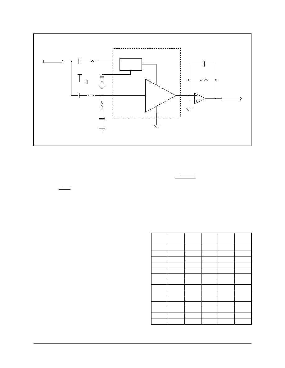
Feedforward Compressor/Limiter
The circuit in Figure 16 shows a typical hard-
knee, feedforward compressor/limiter.
In addition
to compression ratio, the sidechain includes con-
trols for threshold and make-up gain as well.
The Signal Path
The input of the VCA (pin 15) is a virtual ground,
and R14 converts the input signal into a current
flowing into the VCA.
The maximum total signal
current, (I
IN
+ I
OUT
) is 1.8 mA with ±15 V supplies,
so R14 is sized to keep the maximum current at
unity gain to below this level. With peak input volt-
age swing limited by the ±15 V supply rails, the
20 k
resistor at R14 limits maximum i
IN
to about
750 µA. At 0 dB gain, this will cause the same cur-
rent at the VCA output, which is converted back to
15 V by U2 and R13 (also 20 k
). C2 provides AC
coupling, required to block any DC currents that
might otherwise flow into the VCA input. This pre-
vents changes in gain from modulating this current,
which could produce audible "thumps".
The compensation circuit of R28 and C16 is re-
quired for stability. The VCA must "see" a source im-
pedance no greater than 5 k
above 1 MHz. R28 in
parallel with R14 accomplishes this. C16 is chosen
to prevent the added noise gain of the lower source
impedance from increasing noise within the audio
band.
Note that such compensation is unnecessary
when
the
voltage-to-current
converting
resistor
(R14) is 5 k
or less. For example, if the input sig-
nal were limited to lower voltages, the input volt-
age-to-current converting resistor (R14) could be
reduced in value, possibly eliminating the need for
R28 and C16.
U2, along with C4 and R13 forms a trans-
impedance amplifier that converts the VCA's output
current into a voltage. C4 prevents the VCA's output
capacitance from destabilizing the op-amp in this
configuration.
Page 12
THAT4305 Pre-trimmed Low-power Analog Engine
R1
33k
R2
10k
R7
430k
R9
1k
R3
10k
R10
10k
Threshold
Increase
R11
10k
Compression
Ratio
C1
10u
R13
20k
C4
22p NPO
R14
20k
C2
10u
10u
R17
5k1
R18
5k1
C5
100n
R8
620k
R12
10k
Gain
Increase
C13
22u
C15
22p
D1
1N4148
D2
1N4148
-40 dBu
20 dBu
+20 dB
-20 dB
1:1 CR
INF:1 CR
+15V
+15V
C16
100p
R28
6k2
-15V
-15V
-
VCA Out
13
VCA In
15
9
U1A
THAT4305
RMS In
2
RMS Out
5
U1B
THAT4305
U2
U3
U4
C6
22p
+15V
+15V
-15V
Out
In
Vee
Gnd
EC+
Vcc
EC-
11
6
8
12
CT
4
C
TIME
Figure 16. 4305-based feedforward compressor

THAT Corporation; 45 Sumner Street; Milford, Massachusetts 01757-1656; USA
Tel: +1 508 478 9200; Fax: +1 508 478 0990; Web: www.thatcorp.com
Document 600067 Rev 00
Page 13
The Sidechain
As noted earlier, for most effects compressors, it
is best not to linearly compress the entire dynamic
range of the audio signal.
To this end, in the
sidechain of figure 16, we have added a threshold
amplifier with ±30 dB of threshold adjustment.
This restricts compression to signals above the
threshold, passing those below threshold without
any change. Additionally, we added a compression
ratio control adjustable from 1:1 to
:1.
Finally,
we've added a means to apply up to ±20 dB of
static, or "make-up" gain.
The input signal is fed into the RMS detector
through C1 and R1. Like the VCA, the input to the
detector is AC coupled. This prevents any DC cur-
rent flowing into the detector's input from being
measured by the detector.
If unchecked, such off-
sets would limit resolution at low levels, producing
an artificial "floor" to the detector's low-level re-
sponse.
As previously discussed (in the theory section),
the output of the detector is proportional to the log
of the RMS level of the input voltage. The output of
the detector will be approximately zero volts at the
"zero dB reference level" -- the point at which the
RMS value of the input current equals the timing
current (set at 7.5 µA for the 4305). We have chosen
a value of -10dBu, (245 mV
RMS
) for the zero dB ref-
erence level. The required input resistor can be cal-
culated as
R
k
k
mV
A
RMS
=
=
245
7 5
32 6
33
.
.
µ
.
Inverting threshold amplifier (U3) provides gain
of approximately -2 to the detector output signal
above threshold, and zero gain (A
V
=0) to signals be-
low threshold. The change in gain is accomplished
by D1 and D2, which allow negative-going output
signals to pass but block positive-going ones.
Be-
cause U3 is configured to invert, positive-going sig-
nals at the RMS output (indicating increasing ac
input levels) are passed onwards, while nega-
tive-going RMS outputs are blocked.
By feeding
variable dc into this stage via R7 and the threshold
pot R10, we can vary the point at which RMS output
signals begin to be passed through to the threshold
amplifier stage's output (at the junction of D2 and
R2.)
The scaling at the output of the detector is
+6.2 mV/dB, but because R2 is approximately twice
R17, the threshold amplifier (U3) has a gain of -2, so
the scaling at its output is -12.4 mV/dB. To swing
the threshold over ±30 dB, we can calculate the re-
quired value of R7 as follows:
15
0 0124
10
7
30
V
k
R
V
dB
dB
(
)
.
=
.
We can rearrange this to be
10
30
15
7
0 0124
k
R
dB
V
V
dB
=
.
, and therefore,
R
k
7
403 2
=
.
We chose 430 k
for R7.
U4 is a variable-gain inverter that serves to
buffer the VCA's control port, ensuring a low-
impedance drive at that point.
(High impedances,
even as little as 50 to 100 ohms, will increase VCA
distortion at high signal levels.)
Above threshold,
when U4's gain is -Ω, the net gain of the sidechain
(from RMS output to VCA control input) is unity,
and the compression ratio is
:1. The network of
R3, R9, and R11 in conjunction with R18, allows the
gain of U4 to vary from 0 to -1/2, and simultaneously
shapes the (linear) pot's response so that 50% rota-
tion results in 4:1 compression. 4:1 ratio at 50% ro-
tation is often considered a useful target. Note that
with the more conventional approach of connecting
the undriven end of the pot to ground, the compres-
sion ratio at 50% rotation would be 2:1.
Finally, R8 and R12 provide the means for add-
ing static, or "make-up" gain.
The control-voltage
sensitivity at the output of U4 is 6.2 mV/dB. There-
fore,
15
0 0062
5 1
8
20
V
k
R
V
dB
dB
(
)
.
.
=
.
We can rearrange this to be
5 1
20
15
8
0 0062
.
.
k
R
dB
V
V
dB
=
, and therefore,
R
k
k
dB
V
V
dB
8
5
0 0062
20
15
625
=
=
.
We've chosen 620 k
for R8 since it is the near-
est 5% value.

The signals in the sidechain, and at the output of
U4, are generally relatively slow moving, so the
sidechain does not usually require wide bandwidth.
Furthermore, noise on the VCA control port can
modulate the VCA signal, thus adding noise to the
signal path. Accordingly, we added C5 in order re-
duce the noise gain of U4 at high frequencies, which
slightly reduces the high-frequency noise floor of the
entire circuit. C5 may be omitted for non-critical ap-
plications.
As described in the Theory of Operation section
("The RMS Detector - In Brief"), the RMS detector is
capable of driving large spikes of current into the av-
eraging capacitor C
TIME
. To prevent these currents
from upsetting circuit grounds, it is necessary to by-
pass V
CC
to a point very near the grounded end of
C
TIME
with a capacitor equal to or greater than the
value of C
TIME
. This is C13 in Figure 16. The
grounded ends of these two capacitors should be
connected together before being tied to the rest of
the ground system. Doing so will ensure that the
current spikes flow within the local loop consisting
of the two capacitors, and stay out of the ground sys-
tem.
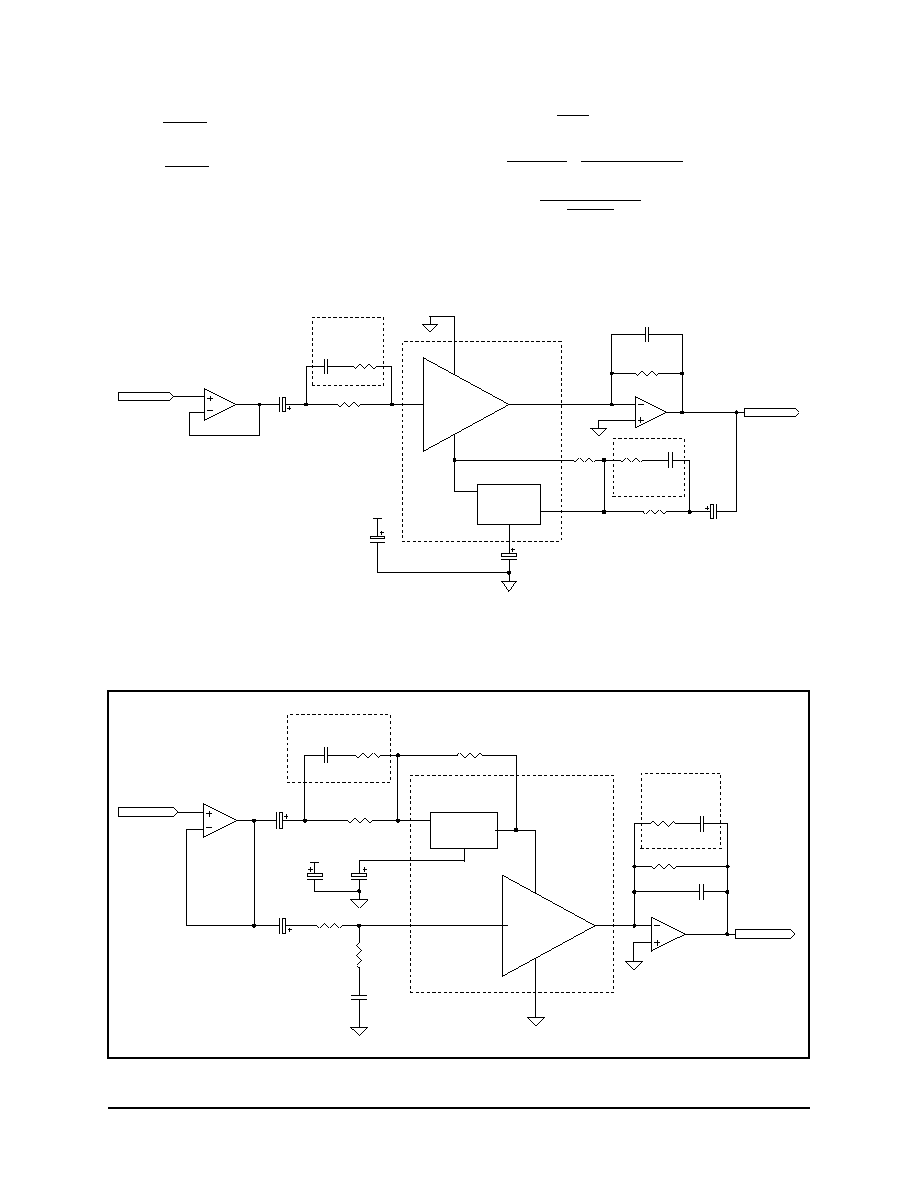
Companding Systems
The Encoder
Figure 17 shows the 4305 configured as a simple
2:1 encoder or feedback compressor. The encoder in
a companding system is positioned before the noisy
channel (wireless link, storage system, etc.). The
static gain of this circuit is 1, or zero dB, and a
5.1 k
resistor (R3) along with a 220 pF capacitor
(C4) comprise the compensation network is re-
quired to keep the VCA's input amplifier stable for
all gains.
Since the RMS detector output is tied directly to
the VCA's E
C-
, the compression ratio will be 2:1.
Note that the use of the negative-sense control port,
E
C-
, makes this circuit a compressor. The RMS de-
tector timing capacitor is set for a release rate of
-125 dB per second by using a value of 10 uF.
As described in the Theory of Operation section
("The RMS Detector - In Brief"), the RMS detector is
capable of driving large spikes of current into the av-
eraging capacitor C
TIME
. To prevent these currents
from upsetting circuit grounds, it is necessary to by-
pass V
CC
to a point very near the grounded end of
the C
TIME
with a capacitor (C5) equal to or greater
than the value of C
TIME
. The grounded ends of these
two capacitors should be connected together before
being tied to the rest of the ground system. Doing so
will ensure that the current spikes flow within the
local loop consisting of the two capacitors, and stay
out of the ground system.
The output of the RMS detector is zero volts
when the RMS input current is equal to the timing
current (internally set to ~7.5 mA). A voltage level
THAT Corporation; 45 Sumner Street; Milford, Massachusetts 01757-1656; USA
Tel: +1 508 478 9200; Fax: +1 508 478 0990; Web: www.thatcorp.com
Page 14
THAT4305 Pre-trimmed Analog Engine
C5
22u
+15V
VCA Out
13
VCA In
15
U1A
THAT4305
RMS In
2
RMS Out
5
U1B
THAT4305
C1
22u
C3
10u
C2
22u
C5
22p
R1
20k
R3
5k1
R4
5k1
R2
20k
C4
220p
U2A
Op-Amp
OUTPUT
INPUT
EC+
EC-
12
11
CT
4
Figure 17. 4305 simple compander circuit - 2:1 encoder (compressor)
of -28.5 dBV was chosen as the desired zero dB ref-
erence. The RMS detector's input resistance can be
calculated as:
R
k
RMS in
A
=
-
10
7 5
28 5
20
5 1
.
.
.
µ
.
This value also applies to the decoder.
The Decoder
Figure 18 shows the THAT4305 configured as a
1:2 expander intended to complement the encoder
in Figure 17.
This circuit also uses a static gain of zero dB.
Since the VCA is not stable unless it sees a high fre-
quency source impedance of 5 k
or less, the com-
pensation network of R13 and C21 ensures stability.
In this instance, the RMS detector output is con-
nected to E
C+
; this reverses the polarity of the con-
trol signal relative to the encoder, and makes this
circuit a 2:1 expander.
System Performance
Table 3 shows the transfer characteristics of this
companding system. The columns labeled Encoder
VCA Gain, Encoder Out, Decoder VCA Gain, and De-
coder Out use the equations derived previously in
the Theory sub-section entitled "The Mathematics of
Log Based Companding Systems". The values in the
column labeled RMS In are derived using the equa-
tion:
I
RMS In
R
Encoder Out
RMS In
=
10
20
(
)
The required encoder VCA gain range is -24 dB
to +36 dB, and the required decoder VCA gain
range is -36 dB to +14 dB. These gains are easily
within the capabilities of the 4305's VCA. The range
of RMS input currents is easily accommodated at
the high end, though accuracy may be slightly com-
promised at the lowest input levels.
THAT Corporation; 45 Sumner Street; Milford, Massachusetts 01757-1656; USA
Tel: +1 508 478 9200; Fax: +1 508 478 0990; Web: www.thatcorp.com
Document 600067 Rev 00
Page 15
C14
22u
+15V
VCA Out
13
VCA In
15
U3A
THAT4305
RMS In
2
RMS Out
5
U3B
THAT4305
C11
22u
C13
10u
C12
22u
C15
47p
R7
20k
R10
5k1
R8
20k
3
2
1
U4A
Op-Amp
INPUT
OUTPUT
R13
5k1
C21
220p
EC+
EC-
12
11
CT
4
Figure 18. 4305 Typical Application Circuit - 1:2 Expander
Encoder
In
Encode
VCA
Gain
Encoder
Out/
Decoder
In
IRMS In
Decoder
VCA
Gain
Decoder
Out
(dBV)
(In dB)
(dBV)
(mA)
(In dB)
(dBV)
+20
-24
-4
0.1223
24
20
+10
-19
-9
0.0688
19
10
0
-14
-14
0.0387
14
0
-10
-9
-19
0.0218
9
-10
-20
-4
-24
0.0122
4
-20
-30
1
-29
0.0069
-1
-30
-40
6
-34
0.0039
-6
-40
-50
11
-39
0.0022
-11
-50
-60
16
-44
0.0012
-16
-60
-70
21
-49
0.0007
-21
-70
-80
26
-54
0.0004
-26
-80
-90
31
-59
0.0002
-31
-90
-100
36
-64
0.0001
84
139
Table 3. 2:1 compander transfer characteristics

Figure 19 tracks signal levels through the en-
coder and decoder of Figures 17 and 18. The en-
coder reduces the dynamic range at its input by a
factor of 2, compressing 120dB into 60dB. The de-
coder expands this dynamic range back to track that
of the encoder's input signal.
Hi-fi Compander
While the previous circuits perform adequately
in some applications, a few minor changes can re-
sult in substantially improved overall performance.
The following compander implementation adds pre-
and de-emphasis to the signal path.
Signal path
pre-emphasis helps overcome the rising noise level
with frequency of an FM RF channel by raising the
level of the high frequency portions of the signal be-
fore it passes through the transmission channel.
Matching signal-path de-emphasis in the decoder
brings the frequency response back to flat while si-
multaneously lowering the noise floor of the chan-
nel.
This helps ensure that isolated low-frequency
signals mask the channel noise by reducing the per-
ception of high-frequency noise signals.
Of
course,
the
drawback
of
signal-path
pre-emphasis is that it can cause overload in the
channel when high-level, high-frequency signals are
present. To guard against this problem, we have
added RMS pre-emphasis to both detectors.
This
mitigates high-frequency overload by lowering the
level-match point to high-frequency signals.
For a
given signal level, high-frequency signals are lowered
in level by the VCA more than low-frequency signals.
As an additional enhancement, we have included
a means to truncate the RMS detector's low-level
response. This improves low level tracking between
different detectors by forcing each detector to "bot-
tom out" at a predetermined level, eliminating the ef-
fects
of
different
low-level
behavior
from
one
detector to the next.
System Performance
The compander shown in Figures 20 and 21 im-
plements all of the aforementioned improvements.
Assuming
no
change
in
VCA
gain
(G
dB
),
the
pre-emphasis network of R3 and C7 produces
~20 dB of signal-path pre-emphasis starting at
~2 kHz and stopping at ~19 kHz.
Note that R3 and C7 also compensate the input
to the VCA, so additional components are not re-
quired to implement this feature. Signal fed to this
network is buffered by U2; while this buffer is not
always necessary, the pre-emphasis network must
be driven from a low source impedance to ensure
proper tracking between the encoder pre-emphasis
and the decoder de-emphasis. If driven from an
unbuffered
source,
the
pre-emphasis
network
should be adjusted to take into account the imped-
ance of that source.
We have included ~10 dB of RMS pre-emphasis
(provided by R5 and C8 in the encoder, and R11 and
C18 in the decoder) for the detectors in both the en-
coder and the decoder. The center frequency of this
pre-emphasis circuit is aligned with the center fre-
quency of the signal path pre-emphasis when evalu-
ated on a logarithmic frequency scale. This shifts the
level match of the encoder symmetrically about the
mid-point of the signal-path pre-emphasis, which
configures the system to take the best advantage of
the companding to avoid high-level high-frequency
overload in the transmission or storage channel.
R6 of the Hi-Fi encoder and R12 of the decoder
are intended to force each of the detectors to stop
responding to low level signals at the same point in
order to improve tracking. This floor occurs when
the RMS current through R1 equals that of R3, and
when the current through R10 equals that of R12.
Since the input of the RMS detector is at virtual
ground, the current through R3 and R12 will be
THAT Corporation; 45 Sumner Street; Milford, Massachusetts 01757-1656; USA
Tel: +1 508 478 9200; Fax: +1 508 478 0990; Web: www.thatcorp.com
Page 16
THAT4305 Pre-trimmed Analog Engine
-100
-80
-60
-40
-20
0
20
20
0
-20
-40
-60
-80
-100
dB
Compression
Process
Expansion
Process
In(Cmp)
Out Exp
Out Cmp
In(Exp)
Figure 19. 2:1 compander transfer characteristics
i
R
RMSOut
R
3
3
=
, and
i
R
RMSOut
R
12
12
=
We'll choose a point about 4dB above the mini-
mum input level which is -56dBV.
V
mV
In
RMS
dBV
=
=
-
10
316
52
20
(
)
.
. Therefore,
0 00316
8 87
23 6
52 0 0062
3
.
.
(
.
(
)) .
mV
k
R
=
-
- -
, And
R
k
k
mV
k
3
459
464
23 6
52 0 0062
0 00316
8 87
=
=
-
- -
(
.
(
)) .
.
.
The same is true for R12.
THAT Corporation; 45 Sumner Street; Milford, Massachusetts 01757-1656; USA
Tel: +1 508 478 9200; Fax: +1 508 478 0990; Web: www.thatcorp.com
Document 600067 Rev 00
Page 17
VCA Out
13
VCA In
15
U3A
THAT4305
RMS In
2
RMS Out
5
U3B
THAT4305
C11
1u
C13
10u
C12
1u
C15
22p
R7
21k0
R10
8k87
R8
84k5
R11
4k02
C17
3n3
C18
3n3
C14
22u
U5
Op-Amp
U4
Op-Amp
V+
Decode In
Decode Out
R9
2k32
R12
464k
R13
5k1
C21
220p
EC+
EC-
12
11
CT
4
Signal Path
De-emphasis
RMS Pre-emphasis
Figure 21. 4305 hi-fi 2:1 decoder circuit
VCA Out
13
VCA In
15
U1A
THAT4305
RMS In 2
RMS Out
5
U1B
THAT4305
C1
1u
C3
10u
C2
1u
C5
22p
R1
21k0
R3
2k32
R4
8k87
R2
84k5
R5
4k02
C7
3n3
C8
3n3
C4
22u
U3
Op-Amp
U2
Op-Amp
Vcc
R6
464k
Encode Out
Encode In
EC+
EC-
12
11
CT
4
Signal Path
Pre-emphasis
RMS
Pre-emphasis
Figure 20. 4305 hi-fi 2:1 encoder circuit
THAT Corporation; 45 Sumner Street; Milford, Massachusetts 01757-1656; USA
Tel: +1 508 478 9200; Fax: +1 508 478 0990; Web: www.thatcorp.com
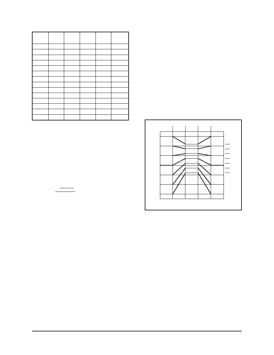
Table 4 shows the transfer characteristics of this
companding system (neglecting the effects of R6 and
R12). As before, the columns labeled Encoder VCA
Gain, Encoder Out, Decoder VCA Gain, and Decoder
Out use the equations derived previously in the sec-
tion
titled
"The
Mathematics
of
Log
Based
Companding Systems". The values in the column la-
beled RMS In are derived using the equation:
I
RMS In
R
Encoder Out
RMS In
=
10
20
(
)
Figure 22 tracks signal levels through the en-
coder and decoder of Figures 20 and 21. The com-
pression and expansion ratios here are the same as
those of the previous circuits, but the frequency
shaping afforded by signal pre- and de-emphasis
and detector pre-emphasis make this a superior
sounding system.
In this application, the VCA gain ranges over
about ±30 dB, which is well within specification, as
is the RMS detector input current.
Other Dynamics Processor Configurations
We have said before that the building blocks con-
tained within the 4305 are applicable to a very wide
range of dynamics processor configurations. These
include companding noise reduction systems with
ratios other (higher or lower) than 2:1:2, multi-band
companders, etc. The 4305 is versatile enough to be
used as the heart of a compressor, expander, noise
gate, AGC, de-esser, frequency-sensitive compres-
sor, and many other dynamics processors. It is be-
yond the scope of this data sheet to provide specific
advice about any of these functional classes. We re-
fer the interested reader to THAT's applications
notebooks volumes 1 and 2, which contain many cir-
cuits based on THAT's other VCAs and RMS level
detectors, but are largely applicable to the 4305 with
only minor variations. Of course, look for more ap-
plications information aimed specifically at the 4305
in the future.
Closing Thoughts
The
design
of
dynamics
processors
and
companding systems is a very intricate art: witness
the proliferation of dynamics processors available in
the market today.
Many of these are based on
THAT's VCAs and level detectors, yet they all have
individual sonic characteristics. In the applications
section of this data sheet, we have offered a few ex-
amples only as starting points. THAT Corporation's
applications engineering department is ready to as-
sist customers with suggestions for tailoring and ex-
tending these basic circuits to meet specific needs.
Page 18
THAT4305 Pre-trimmed Analog Engine
-100
-80
-60
-40
-20
0
20
20
0
-20
-40
-60
-80
-100
dB
Compression
Process
Expansion
Process
In(Cmp)
Out Exp
Out Cmp
In(Exp)
Figure 22. Hi-fi compander transfer characteristics
Encoder
In
Encoder
VCA Gain
Encoder
Out/
Decoder
In
IRMS In
Decoder
VCA Gain
Decoder
Out
(dBV)
(In dB)
(dBV)
(mA)
(In dB)
(dBV)
20
-28
4
0.1841
28
20
10
-23
-1
0.1035
23
10
0
-18
-6
0.0582
18
0
-10
-13
-11
0.0327
13
-10
-20
-8
-16
0.0184
8
-20
-30
-3
-21
0.0104
3
-30
-40
2
-26
0.0058
-2
-40
-50
7
-31
0.0033
-7
-50
-60
12
-36
0.0018
-12
-60
-70
17
-41
0.0010
-17
-70
-80
22
-46
0.0006
-22
-80
-90
27
-51
0.0003
-27
-90
-100
32
-56
0.0002
-32
-100
Table 4. Hi-fi compander transfer characteristics
THAT Corporation; 45 Sumner Street; Milford, Massachusetts 01757-1656; USA
Tel: +1 508 478 9200; Fax: +1 508 478 0990; Web: www.thatcorp.com
Document 600067 Rev 00
Page 19
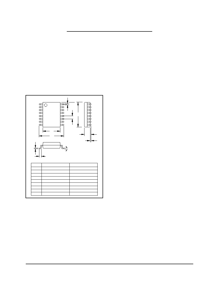
Package and Soldering Information
The THAT 4305 is available in a 16-pin QSOP
package. The package dimensions are shown in Fig-
ure 23 below, while the pinout is given in Table 1 on
page 1.
The 4305 is available only in a lead-free, "green"
package. The lead frame is copper, plated with suc-
cessive layers of nickel palladium, and gold. This
approach makes it possible to solder these devices
using lead-free and lead-bearing solders. The plastic
mold compound, and the material in which the
parts are packaged, contains no hazardous sub-
stances as specified in the RoHS directive. For more
information, including MDDS forms which disclose
the substances contained in our ICs and their pack-
aging, please visit
www.thatcorp.com/RoHShome.html.
The package has been qualified using reflow tem-
peratures as high as 260∞C for 10 seconds. This
makes them suitable for use in a 100% tin solder
process. Furthermore, the 4305 has been qualified
to a JEDEC moisture sensitivity level of MSL1. No
special humidity precautions are required prior to
flow soldering the parts.
A
D
1
B
C
E
I
J
0-8∫
G
H
ITEM
MILLIMETERS
INCHES
A
4.80 - 4.98
0.189 - 0.196
B
3.81 - 3.99
0.150 - 0.157
C
5.79 - 6.20
0.228 - 0.244
D
0.20 - 0.30
0.008 - 0.012
E
0.635 BSC
0.025 BSC
G
1.35 - 1.75
0.0532 - 0.0688
H
0.10 - 0.25
0.004 - 0.010
I
0.40 - 1.27
0.016 - 0.050
J
0.19 - 0.25
0.0075 - 0.0098
Figure 23. QSOP-16 surface mount package drawing

Notes:
THAT Corporation; 45 Sumner Street; Milford, Massachusetts 01757-1656; USA
Tel: +1 508 478 9200; Fax: +1 508 478 0990; Web: www.thatcorp.com
Page 20
THAT4305 Pre-trimmed Analog Engine