THAT Corporation; 45 Sumner Street; Milford, Massachusetts 01757-1656; USA
Tel: +1 508 478 9200; Fax: +1 508 478 0990; Web: www.thatcorp.com
THAT 4311
Description
The THAT 4311 Low Power Dynamics Proces-
sor combines in a single IC all the active circuitry
needed to construct a wide range of dynamics
processors.
The 4311 includes a high perfor-
mance, voltage controlled amplifier, a log re-
sponding RMS-level sensor and three opamps,
one of which is dedicated to the VCA, while the
other two may be used for the signal path or con-
trol voltage processing.
The exponentially-controlled VCA provides
two opposing-polarity, voltage sensitive control
ports. Dynamic range exceeds 105 dB, and THD
is typically 0.09% at 0dB gain. The RMS detector
provides accurate RMS to DC conversion over an
80 dB dynamic range.
Though originally designed for use in micro-
phone noise reduction systems, the 4311 is a use-
ful building block in a number of analog signal
processing applications. The combination of ex-
ponential VCA gain control and logarithmic detec-
tor
response
-
"decibel-linear"
response
-
simplifies the mathematics of designing the con-
trol paths of dynamics processors, making it easy
to develop audio compressors, limiters, gates, ex-
panders, de-essers, duckers, and the like.
The
high level of integration ensures excellent temper-
ature tracking between the VCA and the detector,
while minimizing the external parts count.
T H A T
C o r p o r a t i o n
Low-voltage, Low-power
Analog Engine
�
Dynamics Processor
FEATURES
�
High Performance VCA, RMS-Level
Detector, and three 0pamps in one
package
�
Wide Dynamic Range: >105 dB
�
Low THD: <0.09%
�
Low Power: 7 mA typ.
�
Surface-Mount Package
�
5 VDC Operation
APPLICATIONS
�
Wireless microphone systems
�
Wireless in-ear monitors
�
Compressors and Limiters
�
Gates
�
De-Essers
�
Duckers
18
19
20
17
16
15
14
13
12
11
7
9
8
6
10
5
4
3
2
1
THAT4311
VREF
OA1
OA2
VEE
EC-
EC+
SYM
IN
OUT
IN
CT
OUT
IT
VCA
RMS
OA3
VCC
VREF
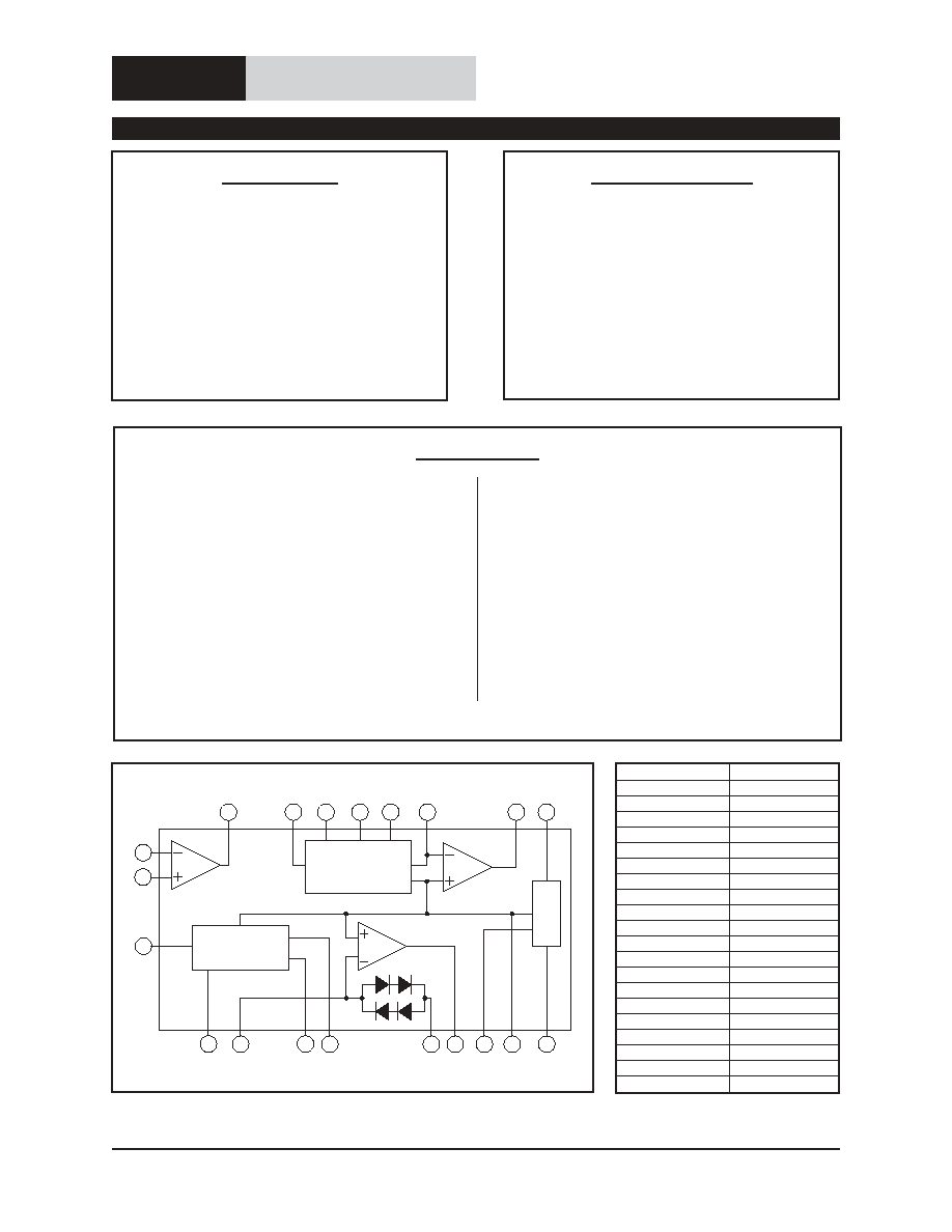
Figure 1. THAT 4311 equivalent block diagram
Pin Name
DMP20
RMS IN
1
IT (I
TIME
)
2
OA2 -IN
3
RMS OUT
4
CT (C
TIME
)
5
CLIP
6
OA2 OUT
7
CAP
8
VREF
9
VEE
10
VCC
11
OA3 OUT
12
VCA OUT
13
SYM
14
EC+
15
EC-
16
VCA IN
17
OA1 OUT
18
OA1 -IN
19
OA1 +IN
20
Table 1. THAT 4311 pin assignments

THAT Corporation; 45 Sumner Street; Milford, Massachusetts 01757-1656; USA
Tel: +1 508 478 9200; Fax: +1 508 478 0990; Web: www.thatcorp.com
Page 2
Low-voltage, Low-power Analog Engine
�
Dynamics Processor
Absolute Maximum Ratings (T
A
= 25�C)
Positive Supply Voltage (V
CC
)
+15 V
Power Dissipation (P
D
) (T
A
= 75�C)
700 mW
Operating Temperature Range (T
OP
)
-20 to +70�C
Storage Temperature Range (T
ST
)
-40 to +125�C
Max
DE
C
E
C+
- (E
C-
)
� 1V
Electrical Characteristics
2
Parameter
Symbol
Conditions
Min
Typ
Max
Units
Supply Current
I
CC
No signal; V
CC
=+7 VDC
--
7.0
9.0
mA
Reference Voltage
V
REF
1.8
1.95
2.1
V
Encode and Decode � Companding Noise Reduction ( V
CC
= +7V encoder, +15V decoder)
Encode Level Match
LMe
Encode mode; f = 1kHz
-25.3
-23.0
-20.7
dBV
Encode Gain Accuracy
Encode mode, f = 1kHz
GAe1
Vin = LMe + 10dB
+3.5
+5
+6.5
dB
GAe2
Vin = LMe - 40dB
-23
-20
-17
dB
Decode Level Match
LMd
Decode mode; f = 1kHz
-18.3
-16.0
-13.7
dB
Decode Gain Accuracy
Decode mode; f=1kHz
GAd1
Vin = LMd + 5dB
+8.5
+10
+11.5
dB
GAd2
Vin = LMd - 20dB
-43
-40
-37
dB
Max Input Voltage
Vime
Encode mode; THD = 3%; f = 1kHz
3
5
--
dBV
Max Output Voltage
Vomd
Decode mode; THD = 3%; f = 1kHz
10.7
13.7
--
dBV
Total Harmonic Distortion
THDtrim
End-to-end; Vin = LMe; f = 1kHz
--
0.025
--
%
(with trim)
Total Harmonic Distortion
THDnotrim
End-to-end; Vin = LMd; f = 1kHz
--
0.15
0.7
%
(no trim)
Output Noise
Vnod
End-to-end ; Vin = short; A-weighted
--
7
--
�Vrms
Recommended Operating Conditions
Parameter
Symbol
Conditions
Min
Typ
Max
Units
Positive Supply Voltage
V
CC
+5
+15
V
SPECIFICATIONS
1
1. All specifications are subject to change without notice.
2. Unless otherwise noted, T
A
=25�C, test circuit as shown in Fig 2.
THAT Corporation; 45 Sumner Street; Milford, Massachusetts 01757-1656; USA
Tel: +1 508 478 9200; Fax: +1 508 478 0990; Web: www.thatcorp.com
Rev. 09/22/03
Page 3
Electrical Characteristics (con't)
Parameter
Symbol
Conditions
Min
Typ
Max
Units
Op amp OA1
Offset Voltage
V
IO
RL = 2k
W
--
�0.5
�6
mV
Equivalent Input Noise
V
nOA1
A-weighted
6.5
10
nV
Hz
Total Harmonic Distortion
THD
OA1
1kHz, A
V
=1; R
L
= 10k
W
--
0.0007
0.003
%
Open Loop Gain
A
VO-OA1
R
L
= 10k
W
--
115
--
Gain Bandwidth Product
GBW
OA1
at 50kHz
--
5
--
Slew Rate
SR
OA1
--
2
--
Op amp OA2
Offset Voltage
V
IO
RL = 2k
W
--
�0.5
�6
mV
Equivalent Input Noise
V
nOA1
A-weighted
7.5
12
nV
Hz
Total Harmonic Distortion
THD
OA1
1kHz, A
V
=1; R
L
= 10k
W
--
0.0007
0.003
%
Open Loop Gain
A
VO-OA1
R
L
= 10k
W
--
110
--
Gain Bandwidth Product
GBW
OA1
at 50kHz
--
5
--
Slew Rate
SR
OA1
--
2
--
R11
23k2
R14
31k6
R22
30R1
R16
280R
C6
47u
V-
R12
261k
R9
51R
5%
R8
300k 5%
R6
20k0
C5
47p NPO
R5
20k0
C4
47u
R7
50k
Sym
cw
V+
R10
100R 5%
C7
10u
R26
100R
5%
TP2
RMS Output
TP1
RMS Input
R17
31k6
C8 47p
R20
10k0
R21
10k0
C9
3u3
1
2
3
CN1
External
Control
Input
CONTROL-VOLTAGE
1
2
3
CN2
Power
Input
C11
100n
(U1)
C10
22u
V+
Bypass
Capacitors
XLR2
XLR-M
Output
C17
47p
D3
1N4004
IN
17
14
15
13
12
16
OUT
VCA
EC+
SYM
EC-
OA3
VREF
U1A
THAT4311
Iset
2
TC
5
IN
1
OUT 4
RMS
U1B
THAT4311
3
7
OA2
VREF
6
U1C
THAT4311
18
19
20 OA1
U1D
THAT4311
CAP
8
VEE
10
VREF
9
VCC
11
VREF
U1E
THAT4311
3
2
6
8
1
U1
OP-27
R1
100k
R4
1k33
R3
10k0
R29
1k33 VREF
R23
280R
R24
2k80
C15
1000u
C16
47u
R27
10k0
R18
10k0
R19
100k
V+
R15
31k6
C19
1000u
C2
10u
C3
22u
C1
10u
V+
VREF
R2
10k0
C12
3u3
+40dB
+20dB
+40dB
+60dB
C18
47u
2
15
SW1B
5
12
SW1E
6
11
SW1F
C14
100n
(U1)
C13
22u
D4
1N4004
V-
V-
VREF
R25
100R
5%
R28
100R 5%
1
16
SW1C
SW1A
1
2
3
CN1
RMS Output
VREF
0dB
5 4
3 1
2
2
3
1
XLR1
XLR-F
Input
5
4
3
1
2
2
3
1
+
+
+
+
+
+
+
+
+
+
+
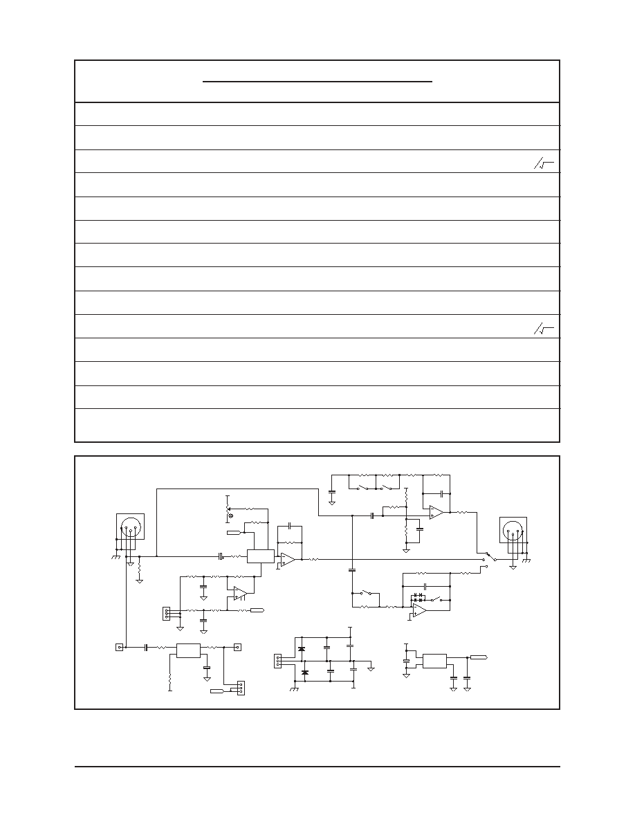
Fig 2. THAT 4311 test circuit
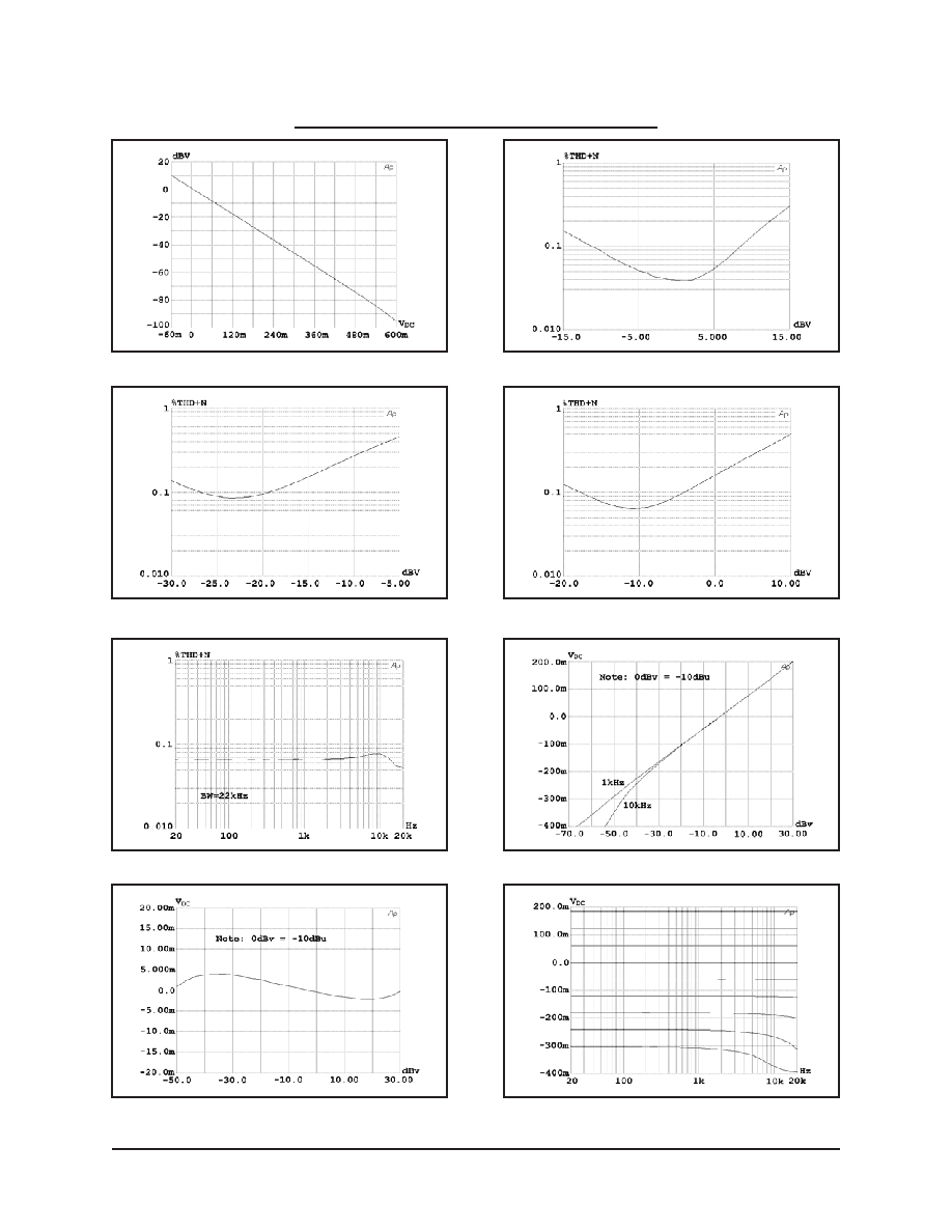
Representative Data (Stand-alone)
THAT Corporation; 45 Sumner Street; Milford, Massachusetts 01757-1656; USA
Tel: +1 508 478 9200; Fax: +1 508 478 0990; Web: www.thatcorp.com
Page 4
Low-voltage, Low-power Analog Engine
�
Dynamics Processor
Fig 3. VCA Gain vs. Control Voltage (Ec-) at 25
�C
Fig 4. VCA 1kHz THD+Noise vs. Input, -15 dB Gain
Fig 5. VCA 1kHz THD+Noise vs. Input, +15 dB Gain
Fig 6. VCA 1kHz THD+Noise vs. Input, 0 dB Gain
Fig 7. VCA THD vs. Frequency, 0 dB gain, 1 Vrms Input
Fig 9. Departure from Ideal Detector Law vs. Level
Fig 8. RMS Output vs. Input Level, 1 kHz & 10 kHz
Fig 10. Detector Output vs. Frequency at Various Levels
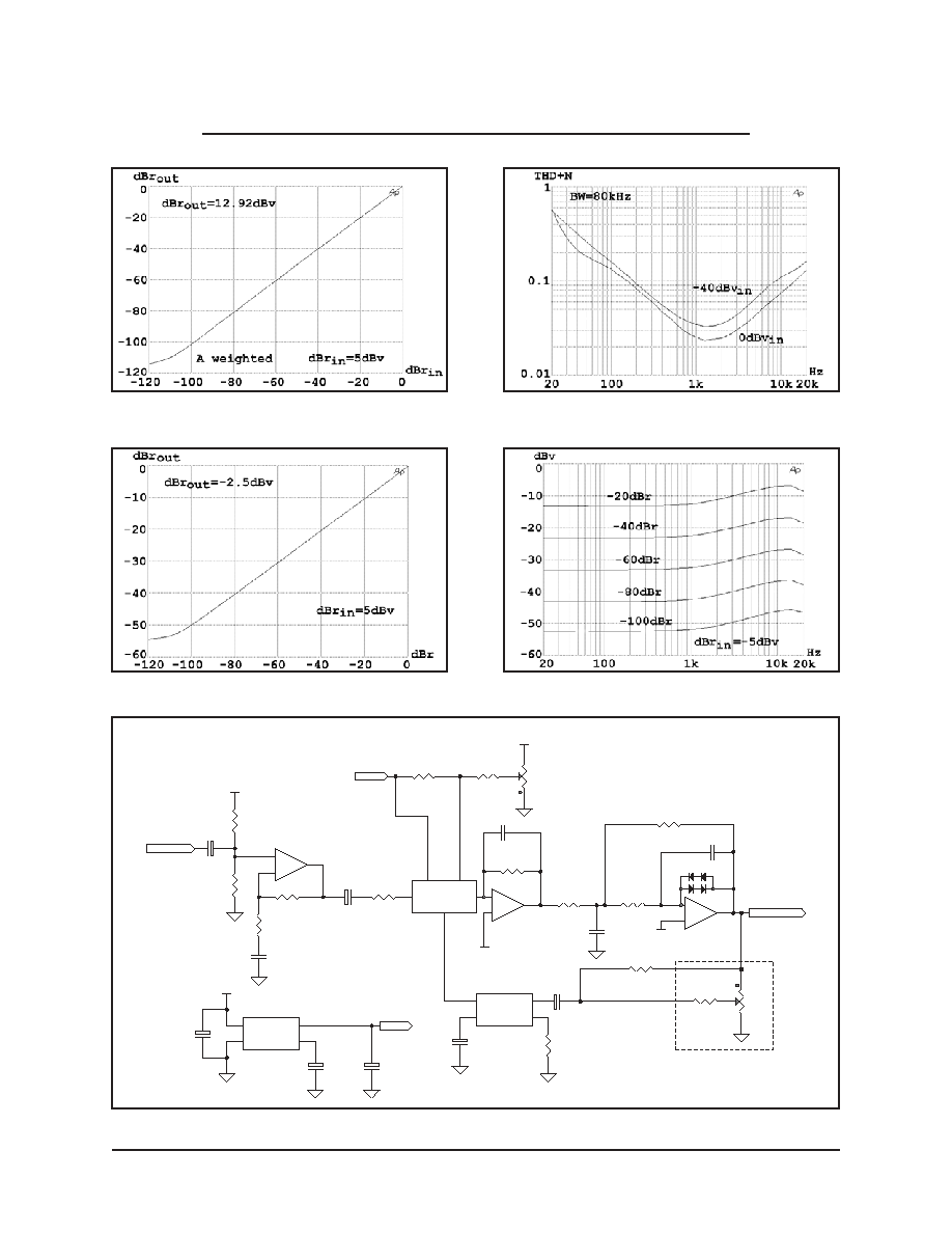
Representative Data (Companding Noise Reduction)
THAT Corporation; 45 Sumner Street; Milford, Massachusetts 01757-1656; USA
Tel: +1 508 478 9200; Fax: +1 508 478 0990; Web: www.thatcorp.com
Rev. 09/22/03
Page 5
Fig 11. End-to-End Transfer Function, 1kHz
Fig 12. End-to-End THD+N
Fig 13. Encoder Transfer Function, 1kHz
Fig 14. Encoder Frequency Response 20-20kHz
IN
17
12
OUT
VCA
EC+
SYM
EC-
OA3
Vref
U1A
THAT4311
Iset
2
TC
5
IN
1
OUT
4
RMS
U1B
THAT4311
3
7
OA2
Vref
6
U1C
THAT4311
18
19
20
U1D
THAT4311
R1
200k
R2
200k
R13
2k
R3
8k06
R5
15k
R9
51R
R8
50k
R6
30k
R11B
10k
R12
261k
C1
10n
C5
270p
C4
3u3
C7
10u
R7
20k
C6
10u
V+
C3
10u
C8
22u
V+
+5
C2
3u3
Encoder
In
Vref
Vref
22kHz 3 pole BW filter
Cap
8
Vee
10
Vref
9
Vcc
11
Vref
U1E
THAT4311
R4
6k19
R10
6k19
C9
570p
Encoder
Out
C16
10u
R31
4k32
C10
4n7
VR1
20k
R11A
20k
optional
15
14
13
16
+
+
+
+
+
+
+
+
_
+
_
_
_
+
Fig 15. THAT 4311 Noise Reduction Encoder Schematic