
THC63LVD103 _Rev2.2
Copyright 2001-2006 THine Electronics, Inc. All rights reserved. 1 THine Electronics, Inc.
THC63LVD103
135MHz 30Bits COLOR LVDS Transmitter
General Description
The THC63LVD103 transmitter is designed to support
pixel data transmission between Host and Flat Panel
Display from NTSC up to SXGA+ resolutions.
The THC63LVD103 converts 35bits of CMOS/TTL
data into LVDS(Low Voltage Differential Signaling)
data stream. The transmitter can be programmed for ris-
ing edge or falling edge clocks through a dedicated pin.
At a transmit clock frequency of 135MHz, 30bits of
RGB data and 5bits of timing and control data
(HSYNC, VSYNC, DE, CNTL1, CNTL2) are transmit-
ted at an effective rate of 945Mbps per LVDS channel.
Features
∑
Wide dot clock range: 8-135MHz suited for NTSC,
VGA, SVGA, XGA,SXGA and SXGA+
∑
PLL requires no external components
∑
Supports spread spectrum clock generator
∑
On chip jitter filtering
∑
Clock edge selectable
∑
Supports reduced swing LVDS for low EMI
∑
Power down mode
∑
Low power single 3.3V CMOS design
∑
64pin TQFP
∑
Backward compatible with
THC63LVDM63R(18bits) / M83R(24bits)
Block Diagram
P
A
RALLEL
T
O
SERIAL
TA +/-
TB +/-
TC +/-
TD +/-
TE +/-
TA0-6
7
CMOS/TTL INPUT
LVDS OUTPUT
RS
CLK IN
(8 to135MHz)
TD0-6
7
TB0-6
PLL
TC0-6
TCLK +/-
(8 to 135MHz)
7
7
7
TE0-6
7
R/F
/PDWN
7
Copyright 2001-2006 THine Electronics, Inc. All rights reserved. 2 THine Electronics, Inc.
THC63LVD103 _Rev2.2
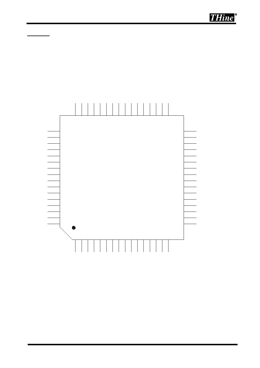
Pin Out
1
2
3
4
5
6
7
8
9
10
11
12
13
14
15
16
48
47 46
45
44
43
42
41
40
39
38
37
36
35
34
33
LVDS GND
LVDS GND
LVDS GND
TE+
TE-
TCLK+
TCLK-
TD+
TD-
LVDS VCC
TC+
TC-
TB+
TB-
TA+
TA-
49
50
51
52
53
54
55
56
57
58
59
60
61
62
63
64
32
31
30
29
28
27
26
25
24
23
22
21
20
19
18
17
GND
GN
D
GN
D
GN
D
GN
D
TA
0
TA
1
TA
2
TA
3
TA
4
TA
5
TA
6
TB5
TB4
TB3 TB2
TB1
TB0
RS
VCC
VCC
TB6
TC1
TC2
TC3
TC3
TC4
TC4
TC4
TC5
TC6
TD0
TC0
TD2
TD1
TD3
TD4
TD
5
TD
6
TE0
TE1
TE2
TE3
TE4
TE5
TE6
R/F
/PD
W
N
PL
L
G
N
D
PL
L
V
C
C
CLK
I
N
Copyright 2001-2006 THine Electronics, Inc. All rights reserved. 3 THine Electronics, Inc.
THC63LVD103 _Rev2.2
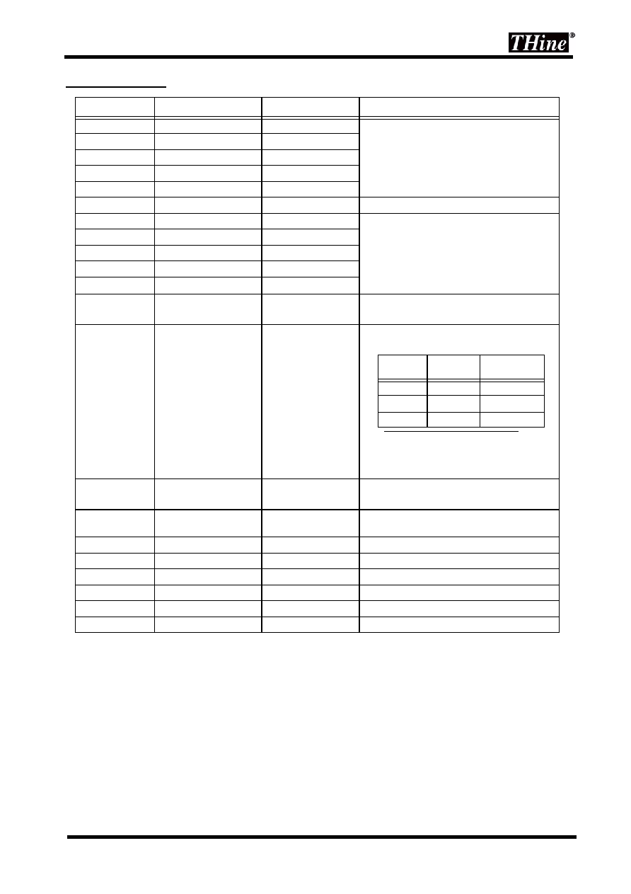
Pin Description
Pin Name
Pin #
Type
Description
TA+, TA-
30, 31
LVDS OUT
LVDS Data Out.
TB+, TB-
28, 29
LVDS OUT
TC+, TC-
24, 25
LVDS OUT
TD+, TD-
20, 21
LVDS OUT
TE+,TE-
18, 19
LVDS OUT
TCLK+, TCLK-
22, 23
LVDS OUT
LVDS Clock Out.
TA0 ~ TA6
33,34,35,36,37,38,40
IN
Pixel Data Inputs.
TB0 ~ TB6
41,42,44,45,46,48,49
IN
TC0 ~ TC6
50,52,53,54,55,57,58
IN
TD0 ~ TD6
59,61,62,63,64,1,3
IN
TE0 ~ TE6
4,5,6,8,9,11,16
IN
/PDWN
13
IN
H: Normal operation,
L: Power down (all outputs are Hi-Z)
RS
43
IN
LVDS swing mode, VREF select.
R/F
60
IN
Input Clock Triggering Edge Select.
H: Rising edge, L: Falling edge
VCC
51, 7
Power
Power Supply Pins for TTL inputs and digital
circuitry.
CLKIN
12
IN
Clock in.
GND
2, 10, 39, 47, 56
Ground
Ground Pins for TTL inputs and digital circuitry.
LVDS VCC
27
Power
Power Supply Pins for LVDS Outputs.
LVDS GND
17, 26, 32
Ground
Ground Pins for LVDS Outputs.
PLL VCC
15
Power
Power Supply Pin for PLL circuitry.
PLL GND
14
Ground
Ground Pins for PLL circuitry.
RS
LVDS
Swing
Small Swing
Input Support
VCC
350mV
N/A
0.6 ~ 1.4V
350mV
RS=VREF
a
a. VREF is Input Reference Voltage.
GND
200mV
N/A

Copyright 2001-2006 THine Electronics, Inc. All rights reserved. 4 THine Electronics, Inc.
THC63LVD103 _Rev2.2
Absolute Maximum Ratings
1
Supply Voltage (V
CC
)
-0.3V ~ +4.0V
CMOS/TTL Input Voltage
-0.3V ~ (V
CC
+ 0.3V)
CMOS/TTL Output Voltage
-0.3V ~ (V
CC
+ 0.3V)
LVDS Driver Output Voltage
-0.3V ~ (V
CC
+ 0.3V)
Junction Temperature
+125
Storage Temperature Range
-55
~ +150
Resistance to soldering heat
+260
/10sec
Maximum Power Dissipation @+25
1.0W
1. "Absolute Maximum Ratings" are those valued beyond which the safety of the device can not be guaranteed.
They are not meant to imply that the device should be operated at these limits. The tables of "Electrical Charac-
teristics" specify conditions for device operation.
∞C
∞C
∞C
∞C
∞C
Copyright 2001-2006 THine Electronics, Inc. All rights reserved. 5 THine Electronics, Inc.
THC63LVD103 _Rev2.2
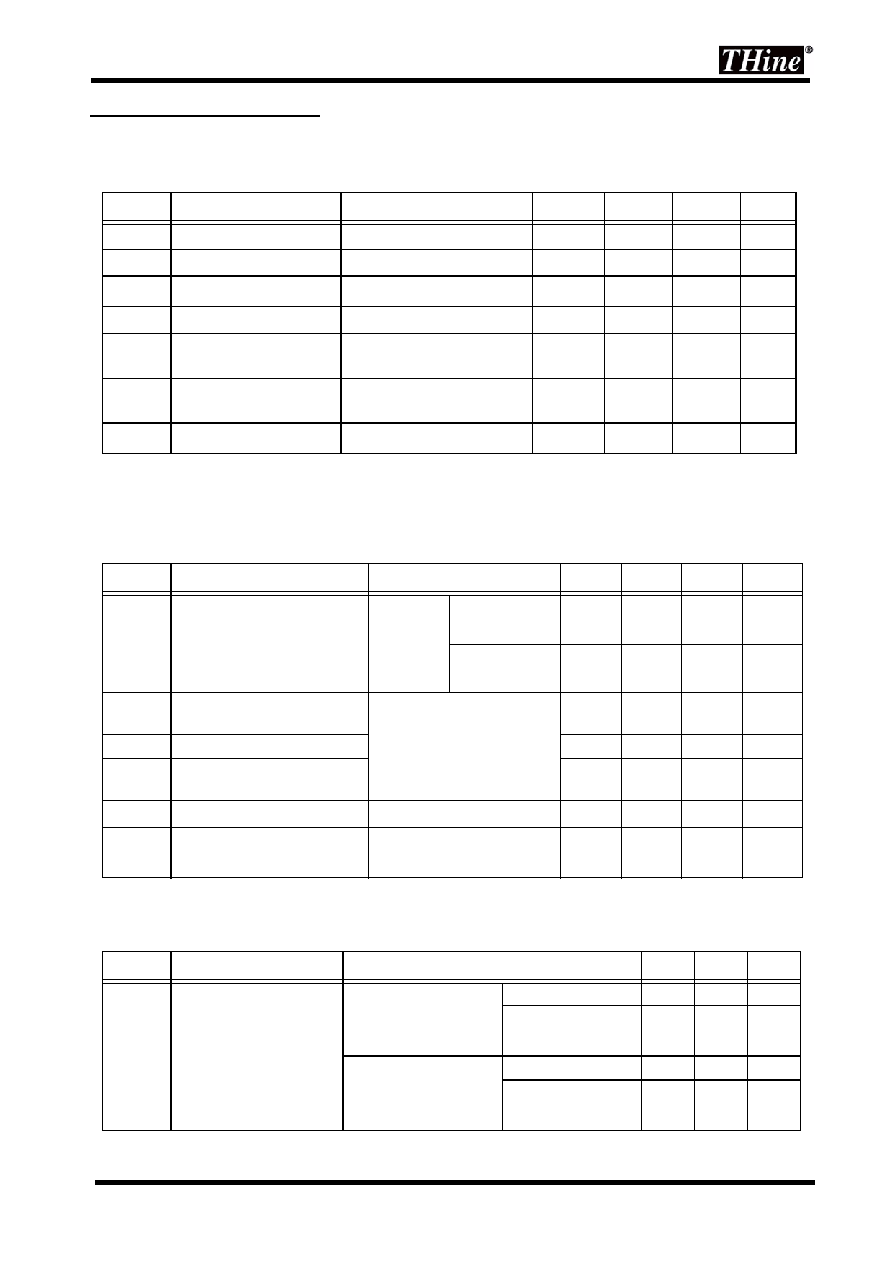
Electrical Characteristics
CMOS/TTL DC Specifications
V
CC
= 3.0V ~ 3.6V, Ta = 0
~ +70
Notes:
1
V
DDQ
voltage defines max voltage of small swing input. It is not an actual input voltage.
2
Small swing signal is applied to TA[6:0], TB[6:0], TC[6:0], TD[6:0], TE[6:0] and CLKIN.
LVDS Transmitter DC Specifications
V
CC
= 3.0V ~ 3.6V, Ta = 0
~ +70
Supply Current
V
CC
= 3.0V ~ 3.6V, Ta =0
~ +70
Symbol
Parameter
Conditions
Min.
Typ.
Max.
Units
V
IH
High Level Input Voltage
RS=VCC or GND
2.0
V
CC
V
V
IL
Low Level Input Voltage
RS=VCC or GND
GND
0.8
V
V
DDQ
1
Small Swing Voltage
1.2
2.8
V
V
REF
Input Reference Voltage
Small Swing (RS=V
DDQ
/2)
V
DDQ
/2
V
SH
2
Small Swing High Level
Input Voltage
V
REF
= V
DDQ
/2
V
DDQ
/2
+100mV
V
V
SL
2
Small Swing Low Level
Input Voltage
V
REF
= V
DDQ
/2
V
DDQ
/2
-100mV
V
I
INC
Input Current
A
Symbol
Parameter
Conditions
Min.
Typ.
Max.
Units
VOD
Differential Output Voltage
RL=100
Normal swing
RS=VCC
250
350
450
mV
Reduced swing
RS=GND
100
200
300
mV
VOD
Change in VOD between
complementary output states
RL=100
35
mV
VOC
Common Mode Voltage
1.125
1.25
1.375
V
VOC
Change in VOC between
complementary output states
35
mV
I
OS
Output Short Circuit Current
VOUT=0V, RL=100
-24
mA
I
OZ
Output TRI-STATE Current
/PDWN=0V,
V
OUT
=0V to VCC
A
Symbol
Parameter
Conditions
Typ.
Max.
Units
I
TCCG
Transmitter Supply
Current
RL=100
,CL=5pF
V
CC
=3.3V, RS=V
CC
Gray Scale Pattern
f=85MHz
58
64
mA
f=135MHz
70
76
mA
RL=100
,CL=5pF
V
CC
=3.3V, RS=GND
Gray Scale Pattern
f=85MHz
44
50
mA
f=135MHz
56
62
mA
∞C
∞C
0V V
IN
V
CC
10
±
∞C
∞C
10
±
∞C
∞C