
THC63LVDF84B/THC63LVDF64B_Rev2.0
Copyright 2001-2003 THine Electronics, Inc. All rights reserved 1 THine Electronics, Inc.
THC63LVDF84B/THC63LVDF64B
LVDS 24Bit/18Bit COLOR HOST-LCD PANEL INTERFACE RECEIVER
General Description
The THC63LVDF84B/THC63LVDF64B receiver sup-
ports wide VCC range(2.5~3.6V). At single 2.5V sup-
ply, the THC63LVDF84B/THC63LVDF64B reduces
EMI and power consumption.
The THC63LVDF84B receiver convert the four
LVDS(Low Voltage Differential Signaling) data streams
back into 28bits of CMOS/TTL data with falling edge
clock.
At a transmit clock frequency of 85MHz, 28bits of RGB
data and 4bits of LCD timing and control data
(HSYNC, VSYNC, CNTL1, CNTL2) are transmitted at
a rate of 2.3Gbps.
Also the THC63LVDF64B receiver convert the three
LVDS data streams back into 21bits of CMOS/TTL data
with falling edge clock.
At a transmit clock frequency of 85MHz, 21bits of RGB
data and 4bits of LCD timing and control data
(HSYNC, VSYNC, CNTL1, CNTL2) are transmitted at
a rate of 1.78Gbps.
Features
∑
Wide VCC range: 2.5~3.6V
∑
Wide dot clock range: 20-85MHz suited for VGA,
SVGA, XGA and SXGA (VCC=3.0~3.6V)
∑
Wide dot clock range: 20-70MHz suited for VGA,
SVGA, XGA and SXGA (VCC=2.5V~3.6V)
∑
PLL requires No external components
∑
Rx power consumption < 80mW @VCC 2.5V,
65MHz Grayscale
∑
Power-Down Mode
∑
Low profile 56 Lead or 48 Lead TSSOP Package
∑
Pin compatible with THC63LVDF84A/F64A
Block Diagram
L
V
D
S
T
O
T
TL
P
A
RA
LL
EL
PLL
RA +/-
RB +/-
RC +/-
RD +/-
RCLK +/-
/PDWN
RA0-6
RC0-6
RD0-6
RECEIVER
(20 to 85MHz)
CMOS/TTL
RB0-6
OUTPUT
CLOCK
(LVDS)
20 to 85MHz
DATA
(LVDS)
(140-595Mbit/On Each LVDS Channel)
7
7
7
7
CLOCK OUT
L
V
D
S
TO
T
T
L
P
A
R
A
LL
EL
PLL
RA +/-
RB +/-
RC +/-
RCLK +/-
/PDWN
RA0-6
RC0-6
RECEIVER
(20 to 85MHz)
CMOS/TTL
RB0-6
OUTPUT
CLOCK
(LVDS)
20 to 85MHz
DATA
(LVDS)
7
7
7
CLOCK OUT
THC63LVDF64B
THC63LVDF84B

Copyright 2001-2003 THine Electronics, Inc. All rights reserved 2 THine Electronics, Inc.
THC63LVDF84B/THC63LVDF64B _Rev2.0
Pin Out
1
2
3
4
5
6
7
8
9
10
11
12
13
14
15
16
17
18
19
20
21
22
23
24
25
26
27
28
56
55
54
53
52
51
50
49
48
47
46
45
44
43
42
41
40
39
38
37
36
35
34
33
32
31
30
29
RC3
RD6
RC4
GND
RC5
RC6
RD0
LVDSGND
RA-
RA+
RB-
RB+
LVDSVCC
LVDSGND
RC-
RC+
RCLK-
RCLK+
RD-
RD+
LVDSGND
PLLGND
PLLVCC
PLLGND
/PDWN
CLKOUT
RA0
GND
VCC
RC2
RC1
RC0
GND
RB6
RD5
RD4
VCC
RB5
RB4
RB3
GND
RB2
RD3
RD2
VCC
RB1
RB0
RA6
GND
RA5
RD1
RA4
RA3
VCC
RA2
RA1
1
2
3
4
5
6
7
8
9
10
11
12
13
14
15
16
17
18
19
20
21
22
23
24
40
39
38
37
36
35
34
33
32
31
30
29
28
27
26
25
RC3
RC4
GND
RC5
RC6
N/C
LVDSGND
RA-
RA+
RB-
RB+
LVDSVCC
LVDSGND
RC-
RC+
RCLK-
RCLK+
LVDSGND
PLLGND
PLLVCC
PLLGND
/PDWN
CLKOUT
RA0
VCC
RC2
RC1
RC0
GND
RB6
VCC
RB5
RB4
RB3
GND
RB2
VCC
RB1
RB0
RA6
GND
RA5
RA4
RA3
VCC
RA2
RA1
GND
41
42
43
44
45
46
47
48
THC63LVDF84B
THC63LVDF64B

Copyright 2001-2003 THine Electronics, Inc. All rights reserved 3 THine Electronics, Inc.
THC63LVDF84B/THC63LVDF64B _Rev2.0
THC63LVDF84B Pin Description
THC63LVDF64B Pin Description
Pin Name
Pin #
Type
Description
RA+, RA-
9, 10
LVDS IN
LVDS Data Inputs
RB+, RB-
11, 12
LVDS IN
RC+, RC-
15, 16
LVDS IN
RD+, RD-
19, 20
LVDS IN
RCLK+, RCLK-
17, 18
LVDS IN
LVDS Clock Inputs
RA0~RA6
27,29,30,32,33,35,37
OUT
Pixel Data Outputs
RB0~RB6
38,39,43,45,46,47,51
OUT
RC0~RC6
53,54,55,1,3,5,6
OUT
RD0~RD6
7,34,41,42,49,50,2
OUT
CLKOUT
26
OUT
Pixel Clock Output
/PDWN
25
IN
H: Normal operation
L: Power down (all outputs are pulled to ground )
VCC
31,40,48,56
Power
Power Supply Pins for TTL outputs and digital circuitry
GND
4,28,36,44,52
Ground
Ground Pins for TTL outputs and digital circuitry
LVDSVCC
13
Power
Power Supply Pin for LVDS inputs
LVDSGND
8,14,21
Ground
Ground Pins for LVDS inputs
PLLVCC
23
Power
Power Supply Pin for PLL circuitry
PLLGND
22,24
Ground
Ground Pins for PLL circuitry
Pin name
Pin #
Type
Description
RA+, RA-
8,9
LVDS IN
LVDS Data Inputs
RB+, RB-
10,11
LVDS IN
RC+, RC-
14,15
LVDS IN
RCLK+, RCLK-
16,17
LVDS IN
LVDS Clock Inputs
RA0~RA6
24,26,27,29,30,31,33
OUT
Pixel Data Outputs
RB0~RB6
34,35,37,39,40,41,43
OUT
RC0~RC6
45,46,47,1,2,4,5
OUT
CLKOUT
23
OUT
Pixel Clock Output
/PDWN
22
IN
H: Normal operation
L: Power down ( all outputs are pulled to ground)
VCC
28,36,42,48
Power
Power Supply Pins for TTL outputs and digital circuitry
GND
3,25,32,38,44
Ground
Ground Pins for TTL outputs and digital circuitry
LVDSVCC
12
Power
Power Supply Pin for LVDS inputs
LVDSGND
7,13,18
Ground
Ground Pins for LVDS inputs
PLLVCC
20
Power
Power Supply Pin for PLL circuitry
PLLGND
19,21
Ground
Ground Pins for PLL circuitry

Copyright 2001-2003 THine Electronics, Inc. All rights reserved 4 THine Electronics, Inc.
THC63LVDF84B/THC63LVDF64B _Rev2.0
Electrical Characteristics
CMOS/TTL DC SPECIFICATIONS
VCC = 2.5V ~ 3.6V, Ta = -10
~ +70
LVDS RECEIVER DC SPECIFICATIONS
VCC = 2.5V ~ 3.6V, Ta = -10
~ +70
Absolute Maximum Ratings
1
Supply Voltage (Vcc) -0.3 to +4V
CMOS/TTL Input Voltage -0.3 to (Vcc + 0.3V)
CMOS/TTL Output Voltage -0.3V to (Vcc + 0.3V)
LVDS Receiver Input Voltage -0.3V to (Vcc + 0.3V)
Junction Temperature +125
Storage Temperature Range -55
to +150
Resistance to soldering heat +260
/10sec
Maximum Power Dissipation@25
0.5W
Symbol
Parameter
Conditions
Min.
Typ.
Max.
Units
V
IH
High Level Input Voltage
2.0
VCC
V
V
IL
Low Level Input Voltage
GND
0.8
V
V
OH1
High Level Output Voltage
VCC= 3.0V ~ 3.6V
I
OH
= -4mA
2.4
V
V
OL1
Low Level Output Voltage
VCC = 3.0V ~ 3.6V
I
OL
= 4mA
0.4
V
V
OH2
High Level Output Voltage
VCC= 2.5V ~ 3.0V
I
OH
= -2mA
2.1
V
V
OL2
Low Level Output Voltage
VCC = 2.5V ~ 3.0V
I
OL
= 2mA
0.4
V
I
IN
Input Current
uA
Symbol
Parameter
Conditions
Min.
Typ.
Max.
Units
V
TH
Differential Input High Threshold
VOC = +1.2V
100
mV
V
TL
Differential Input Low Threshold
-100
mV
I
IN
Input Current
V
IN
= +2.4V/0V
VCC = 3.6V
uA
1. "Absolute Maximum Ratings" are those valued beyond which the safety of the device can not be guaranteed. They
are not meant to imply that the device should be operated at these limits. The tables of "Electrical Characteristics"
specify conditions for device operation.
∞C
∞C
0V VIN VCC
£
£
10
±
∞C
∞C
10
±
∞C
∞C
∞C
∞C
∞C
Copyright 2001-2003 THine Electronics, Inc. All rights reserved 5 THine Electronics, Inc.
THC63LVDF84B/THC63LVDF64B _Rev2.0
Supply Current
VCC = 2.5V ~ 3.6V, Ta = -10
~ +70
Symbol
Parameter
Condition(*)
Typ.
Max.
Units
I
RCCG
Receiver Supply Current
16Grayscale Pattern
CL=8pF, VCC=3.3V
f = 65MHz
41
53
mA
f = 85MHz
52
64
mA
CL=8pF, VCC=2.5V
f = 65MHz
30
42
mA
I
RCCW
Receiver Supply Current
Worst Case Pattern
CL=8pF, VCC=3.3V
f = 65MHz
72
94
mA
f = 85MHz
84
96
mA
CL=8pF, VCC=2.5V
f = 65MHz
42
64
mA
I
RCCS
Receiver Power Down
Supply Current
/PDWN = L
10
µA
∞C
∞C
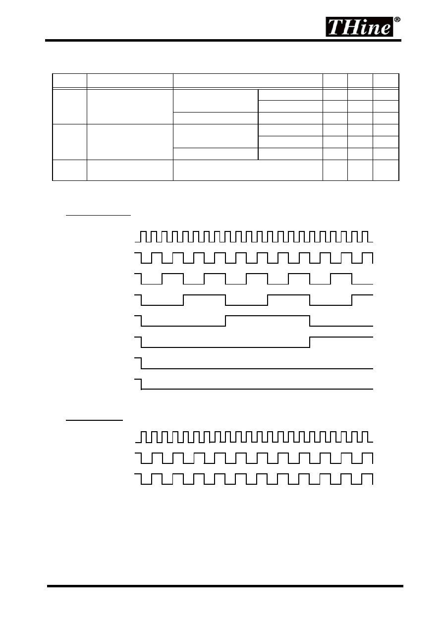
CLKIN
Rx0
Rx1
Rx2
Rx3
Rx4
Rx5
Rx6
16 Gray Scale Pattern
CLKIN
EVEN RxIN
ODD RxIN
Worst Case Pattern