 | –≠–ª–µ–∫—Ç—Ä–æ–Ω–Ω—ã–π –∫–æ–º–ø–æ–Ω–µ–Ω—Ç: 26LS31 | –°–∫–∞—á–∞—Ç—å:  PDF PDF  ZIP ZIP |
AM26LS31C
QUADRUPLE DIFFERENTIAL LINE DRIVER
SLLS114D ≠ JANUARY 1979 ≠ REVISED OCTOBER 1998
1
POST OFFICE BOX 655303
∑
DALLAS, TEXAS 75265
D
Meets or Exceeds the Requirements of
ANSI TIA/EIA-422-B and ITU
Recommendation V.11
D
Operates From a Single 5-V Supply
D
TTL Compatible
D
Complementary Outputs
D
High Output Impedance in Power-Off
Conditions
D
Complementary Output-Enable Inputs
description
The AM26LS31C is a quadruple complementary-output line driver designed to meet the requirements of
ANSI TIA/EIA-422-B and ITU (formerly CCITT) Recommendation V.11. The 3-state outputs have high-current
capability for driving balanced lines such as twisted-pair or parallel-wire transmission lines, and they provide
a high-impedance state in the power-off condition. The enable function is common to all four drivers and offers
the choice of an active-high or active-low enable (G, G) input. Low-power Schottky circuitry reduces power
consumption without sacrificing speed.
The AM26LS31C is characterized for operation from 0
∞
C to 70
∞
C.
FUNCTION TABLE
(each driver)
INPUT
ENABLES
OUTPUTS
A
G
G
Y
Z
H
H
X
H
L
L
H
X
L
H
H
X
L
H
L
L
X
L
L
H
X
L
H
Z
Z
H = high level, L = low level, X = irrelevant,
Z = high impedance (off)
Copyright
©
1998, Texas Instruments Incorporated
PRODUCTION DATA information is current as of publication date.
Products conform to specifications per the terms of Texas Instruments
standard warranty. Production processing does not necessarily include
testing of all parameters.
Please be aware that an important notice concerning availability, standard warranty, and use in critical applications of
Texas Instruments semiconductor products and disclaimers thereto appears at the end of this data sheet.
1
2
3
4
5
6
7
8
16
15
14
13
12
11
10
9
1A
1Y
1Z
G
2Z
2Y
2A
GND
V
CC
4A
4Y
4Z
G
3Z
3Y
3A
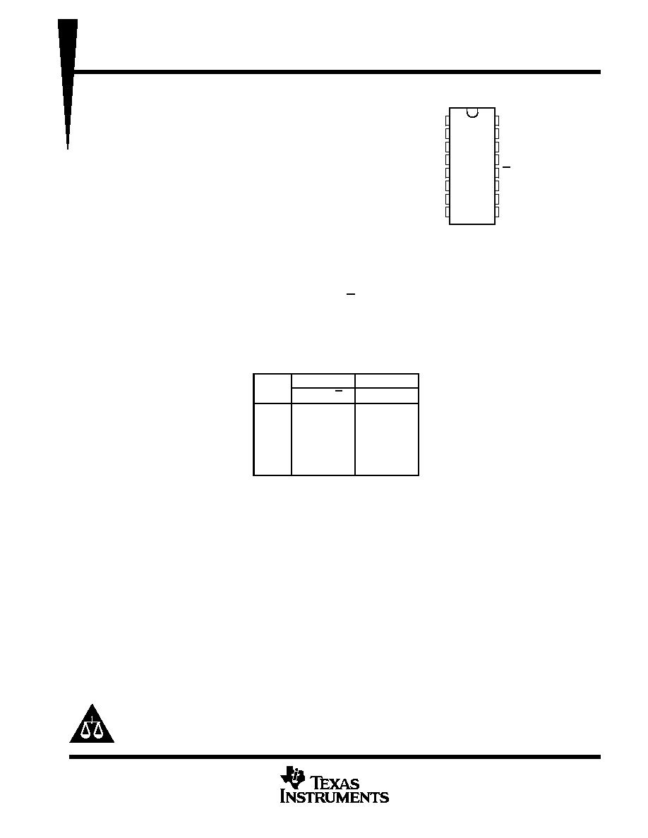
D OR N PACKAGE
(TOP VIEW)

AM26LS31C
QUADRUPLE DIFFERENTIAL LINE DRIVER
SLLS114D ≠ JANUARY 1979 ≠ REVISED OCTOBER 1998
2
POST OFFICE BOX 655303
∑
DALLAS, TEXAS 75265
logic symbol
4
G
12
1Y
2
1Z
3
1
1A
1
EN
2Y
6
2Z
5
7
2A
3Y
10
3Z
11
9
3A
4Y
14
4Z
13
15
4A
G
logic diagram (positive logic)
1Z
1Y
G
G
1A
4
12
1
2
3
2Z
2Y
2A
7
6
5
3Z
3Y
3A
9
10
11
4Z
4Y
4A
15
14
13
AM26LS31C
QUADRUPLE DIFFERENTIAL LINE DRIVER
SLLS114D ≠ JANUARY 1979 ≠ REVISED OCTOBER 1998
3
POST OFFICE BOX 655303
∑
DALLAS, TEXAS 75265
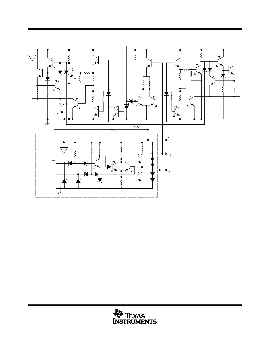
schematic (each driver)
22 k
To Three Other Drivers
Common to All Four Drivers
GND
Enable G
Enable G
VCC
V
V
Output Y
9
Input A
22 k
22 k
All resistor values are nominal.
Output Z
9
absolute maximum ratings over operating free-air temperature range (unless otherwise noted)
Supply voltage, V
CC
(see Note 1)
7 V
. . . . . . . . . . . . . . . . . . . . . . . . . . . . . . . . . . . . . . . . . . . . . . . . . . . . . . . . . . . . .
Input voltage, V
I
7 V
. . . . . . . . . . . . . . . . . . . . . . . . . . . . . . . . . . . . . . . . . . . . . . . . . . . . . . . . . . . . . . . . . . . . . . . . . . . .
Output off-state voltage
5.5 V
. . . . . . . . . . . . . . . . . . . . . . . . . . . . . . . . . . . . . . . . . . . . . . . . . . . . . . . . . . . . . . . . . . . .
Package thermal impedance,
JA
(see Note 2): D package
113
∞
C/W
. . . . . . . . . . . . . . . . . . . . . . . . . . . . . . . . . .
N package
78
∞
C/W
. . . . . . . . . . . . . . . . . . . . . . . . . . . . . . . . . . .
Storage temperature range, T
stg
≠65
∞
C
to 150
∞
C
. . . . . . . . . . . . . . . . . . . . . . . . . . . . . . . . . . . . . . . . . . . . . . . . . . .
Lead temperature 1,6 mm (1/16 inch) from case for 10 seconds
260
∞
C
. . . . . . . . . . . . . . . . . . . . . . . . . . . . . . .
Stresses beyond those listed under "absolute maximum ratings" may cause permanent damage to the device. These are stress ratings only, and
functional operation of the device at these or any other conditions beyond those indicated under "recommended operating conditions" is not
implied. Exposure to absolute-maximum-rated conditions for extended periods may affect device reliability.
NOTES:
1. All voltage values, except differential output voltage VOD, are with respect to network GND.
2. The package thermal impedance is calculated in accordance with JESD 51, except for through-hole packages, which use a trace
length of zero.

AM26LS31C
QUADRUPLE DIFFERENTIAL LINE DRIVER
SLLS114D ≠ JANUARY 1979 ≠ REVISED OCTOBER 1998
4
POST OFFICE BOX 655303
∑
DALLAS, TEXAS 75265
recommended operating conditions (unless otherwise noted)
MIN
NOM
MAX
UNIT
Supply voltage, VCC
4.75
5
5.25
V
High-level input voltage, VIH
2
V
Low-level input voltage, VIL
0.8
V
High-level output current, IOH
≠20
mA
Low-level output current, IOL
20
mA
Operating free-air temperature, TA
0
70
∞
C
electrical characteristics over operating free-air temperature range (unless otherwise noted)
PARAMETER
TEST CONDITIONS
MIN
TYP
MAX
UNIT
VIK
Input clamp voltage
VCC = 4.75 V,
II = ≠18 mA
≠1.5
V
VOH
High-level output voltage
VCC = 4.75 V,
IOH = ≠20 mA
2.5
V
VOL
Low-level output voltage
VCC = 4.75 V,
IOL = 20 mA
0.5
V
IOZ
Off state (high impedance state) output current
VCC = 4 75 V
VO = 0.5 V
≠20
µ
A
IOZ
Off-state (high-impedance-state) output current
VCC = 4.75 V
VO = 2.5 V
20
µ
A
II
Input current at maximum input voltage
VCC = 5.25 V,
VI = 7 V
0.1
mA
IIH
High-level input current
VCC = 5.25 V,
VI = 2.7 V
20
µ
A
IIL
Low-level input current
VCC = 5.25 V,
VI = 0.4 V
≠0.36
mA
IOS
Short-circuit output current
VCC = 5.25 V
≠30
≠150
mA
ICC
Supply current
VCC = 5.25 V,
All outputs disabled
32
80
mA
All typical values are at VCC = 5 V and TA = 25
∞
C.
Not more than one output should be shorted at a time, and duration of the short circuit should not exceed one second.
switching characteristics, V
CC
= 5 V, T
A
= 25
∞
C (see Figure 1)
PARAMETER
TEST CONDITIONS
MIN
TYP
MAX
UNIT
tPLH
Propagation delay time, low-to-high-level output
CL = 30 pF
S1 and S2 open
14
20
ns
tPHL
Propagation delay time, high-to-low-level output
CL = 30 pF,
S1 and S2 open
14
20
ns
tPZH
Output enable time to high level
CL = 30 pF
RL = 75
25
40
ns
tPZL
Output enable time to low level
CL = 30 pF
RL = 180
37
45
ns
tPHZ
Output disable time from high level
CL = 10 pF
S1 and S2 closed
21
30
ns
tPLZ
Output disable time from low level
CL = 10 pF,
S1 and S2 closed
23
35
ns
Output-to-output skew
CL = 30 pF,
S1 and S2 open
1
6
ns

AM26LS31C
QUADRUPLE DIFFERENTIAL LINE DRIVER
SLLS114D ≠ JANUARY 1979 ≠ REVISED OCTOBER 1998
5
POST OFFICE BOX 655303
∑
DALLAS, TEXAS 75265
PARAMETER MEASUREMENT INFORMATION
Waveform 1
(see Note E)
Output Z
Output Y
Input A
(see Notes B
and C)
VOL
VOH
VOL
VOH
3 V
tPHL
Skew
Skew
tPLH
tPLH
tPHL
0 V
PROPAGATION DELAY TIMES AND SKEW
TEST CIRCUIT
VCC
Test Point
S1
S2
75
180
CL
(see Note A)
From Output
Under Test
VOH
VOL
1.5 V
0 V
3 V
Enable G
Enable G
(see Note D)
S1 Open
S2 Closed
S1 Closed
S2 Open
tPZH
tPZL
tPHZ
tPLZ
S1 Closed
S2 Closed
0.5 V
0 V
4.5 V
S1 Closed
S2 Closed
1.5 V
ENABLE AND DISABLE TIME WAVEFORMS
See Note D
NOTES: A. CL includes probe and jig capacitance.
B. All input pulses are supplied by generators having the following characteristics: PRR
1 MHz, ZO
50
, tr
15 ns, tf
6 ns.
C. When measuring propagation delay times and skew, switches S1 and S2 are open.
D. Each enable is tested separately.
E. Waveform 1 is for an output with internal conditions such that the output is low except when disabled by the output control.
Waveform 2 is for an output with internal conditions such that the output is high except when disabled by the output control.
1.3 V
1.3 V
1.5 V
1.5 V
1.5 V
1.5 V
Waveform 2
(see Note E)
0.5 V
1.5 V
1.5 V
Figure 1. Test Circuit and Voltage Waveforms