 | –≠–ª–µ–∫—Ç—Ä–æ–Ω–Ω—ã–π –∫–æ–º–ø–æ–Ω–µ–Ω—Ç: 54AC11175 | –°–∫–∞—á–∞—Ç—å:  PDF PDF  ZIP ZIP |
54AC11175, 74AC11175
QUADRUPLE D-TYPE FLIP-FLOPS
WITH CLEAR
SCAS090 ≠ DECEMBER 1989 ≠ REVISED APRIL 1993
POST OFFICE BOX 655303
∑
DALLAS, TEXAS 75265
Copyright
©
1993, Texas Instruments Incorporated
2≠1
∑
Applications Include: Buffer/Storage
Registers, Shift Registers, Pattern
Generators
∑
Flow-Through Architecture Optimizes
PCB Layout
∑
Center-Pin V
CC
and GND Configurations
Minimize High-Speed Switching Noise
∑
EPIC
t
(Enhanced-Performance Implanted
CMOS) 1-
m
m Process
∑
500-mA Typical Latch-Up Immunity at 125
∞
C
∑
Package Options Include Plastic
Small-Outline Packages, Ceramic Chip
Carriers, and Standard Plastic and Ceramic
300-mil DIPs
description
These positive-edge-triggered flipflops implement
D-type flip-flop logic with a direct clear input.
Information at the D inputs that meets the setup
time requirements is transferred to the outputs on
the positive-going edge of the clock pulse. Clock
triggering occurs at a particular voltage level and
is not directly related to the transition time of the
positive-going pulse. When the clock input is at
either the high or low level, the D input signal has
no effect at the output.
The 54AC11175 is characterized for operation
over the full military temperature range of ≠ 55
∞
C
to 125
∞
C. The 74AC11175 is characterized for
operation from ≠ 40
∞
C to 85
∞
C.
FUNCTION TABLE
(each flip-flop)
INPUTS
OUTPUTS
CLR
CLK
D
Q
Q
L
X
X
L
H
H
H
H
L
H
L
L
H
H
L
X
Q0
Q0
1
2
3
4
5
6
7
8
9
10
20
19
18
17
16
15
14
13
12
11
1Q
2Q
2Q
GND
GND
GND
GND
3Q
3Q
4Q
1Q
CLR
1D
2D
V
CC
V
CC
3D
4D
CLK
4Q
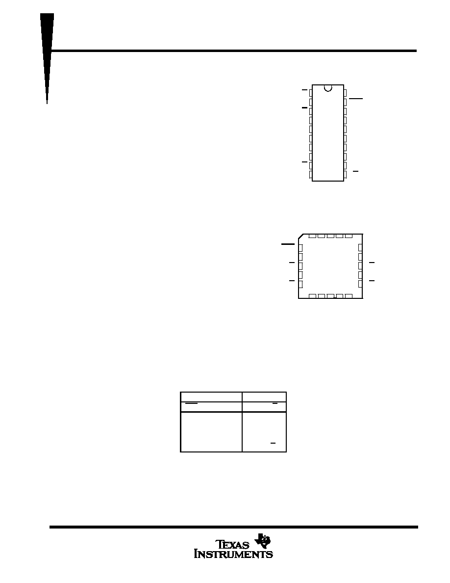
54AC11175 . . . J PACKAGE
74AC11175 . . . DW or N PACKAGE
(TOP VIEW)
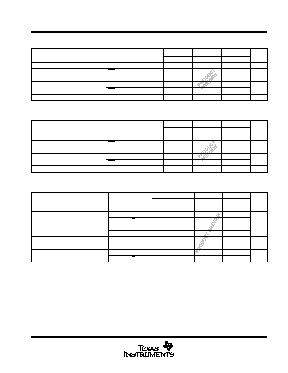
54AC11014 . . . FK PACKAGE
(TOP VIEW)
3
2
1 20 19
9 10 11 12 13
4
5
6
7
8
18
17
16
15
14
4D
CLK
4Q
4Q
3Q
CLR
1Q
1Q
2Q
2Q
1D
GND
3D
GND
CND
CC
V
2D
3Q
GND
CC
V
EPIC is a trademark of Texas Instruments Incorporated.
UNLESS OTHERWISE NOTED this document contains PRODUCTION
DATA information current as of publication date. Products conform to
specifications per the terms of Texas Instruments standard warranty.
Production processing does not necessarily include testing of all
parameters.

54AC11175, 74AC11175
QUADRUPLE D-TYPE FLIP-FLOPS
WITH CLEAR
SCAS090 ≠ DECEMBER 1989 ≠ REVISED APRIL 1993
POST OFFICE BOX 655303
∑
DALLAS, TEXAS 75265
2≠2
logic symbol
logic diagram (positive logic)
CLK
1D
2D
3D
19
12
18
17
14
9
8
3
2
1
20
1D
R
C1
CLR
1D
CLK
2D
3D
4D
C1
C1
C1
C1
R
R
R
R
1D
1D
1D
1D
CLR
19
12
18
17
14
13
20
1
1Q
1Q
2
3
2Q
2Q
8
9
3Q
3Q
10
11
4Q
4Q
This symbol is in accordance with ANSI/IEEE Std 91-1984
and IEC Publication 617-12.
Pin numbers shown are for the DW, J and N packages.
4D
13
11
10
1Q
1Q
2Q
2Q
3Q
4Q
4Q
3Q
absolute maximum ratings over operating free-air temperature range (unless otherwise noted)
Supply voltage range, V
CC
≠ 0.5 V to 7 V
. . . . . . . . . . . . . . . . . . . . . . . . . . . . . . . . . . . . . . . . . . . . . . . . . . . . . . . . . .
Input voltage range, V
I
(see Note 1)
≠ 0.5 V to V
CC
+ 0.5 V
. . . . . . . . . . . . . . . . . . . . . . . . . . . . . . . . . . . . . . . . . . .
Output voltage range, V
O
(see Note 1)
≠ 0.5 V to V
CC
+ 0.5 V
. . . . . . . . . . . . . . . . . . . . . . . . . . . . . . . . . . . . . . . .
Input clamp current, I
IK
(V
I
< 0 or V
I
> V
CC
)
±
20 mA
. . . . . . . . . . . . . . . . . . . . . . . . . . . . . . . . . . . . . . . . . . . . . . . . .
Output clamp current, I
OK
(V
O
< 0 or V
O
> V
CC
)
±
50 mA
. . . . . . . . . . . . . . . . . . . . . . . . . . . . . . . . . . . . . . . . . . . .
Continuous output current, I
O
(V
O
= 0 to V
CC
)
±
50 mA
. . . . . . . . . . . . . . . . . . . . . . . . . . . . . . . . . . . . . . . . . . . . . .
Continuous current through V
CC
or GND
±
200 mA
. . . . . . . . . . . . . . . . . . . . . . . . . . . . . . . . . . . . . . . . . . . . . . . . . .
Storage temperature range
≠ 65
∞
C to 150
∞
C
. . . . . . . . . . . . . . . . . . . . . . . . . . . . . . . . . . . . . . . . . . . . . . . . . . . . . . . .
}
Stresses beyond those listed under "absolute maximum ratings" may cause permanent damage to the device. These are stress ratings only and
functional operation of the device at these or any other conditions beyond those indicated under "recommended operating conditions" is not
implied. Exposure to absolute-maximum-rated conditions for extended periods may affect device reliability.
NOTE 1: The input and output voltage ratings may be exceeded if the input and output current ratings are observed.

54AC11175, 74AC11175
QUADRUPLE D-TYPE FLIP-FLOPS
WITH CLEAR
SCAS090 ≠ DECEMBER 1989 ≠ REVISED APRIL 1993
POST OFFICE BOX 655303
∑
DALLAS, TEXAS 75265
2≠3
recommended operating conditions
54AC11175
74AC11175
UNIT
MIN
NOM
MAX
MIN
NOM
MAX
UNIT
VCC
Supply voltage
3
5
5.5
3
5
5.5
V
VCC = 3 V
2.1
2.1
VIH
High-level input voltage
VCC = 4.5 V
3.15
3.15
V
VCC = 5.5 V
3.85
3.85
VCC = 3 V
0.9
0.9
VIL
Low-level input voltage
VCC = 4.5 V
1.35
1.35
V
VCC = 5.5 V
1.65
1.65
VCC = 3 V
≠ 4
≠ 4
IOH
High-level output current
VCC = 4.5 V
≠ 24
≠ 24
mA
VCC = 5.5 V
≠ 24
≠ 24
VCC = 3 V
12
12
IOL
Low-level output current
VCC = 4.5 V
24
24
mA
VCC = 5.5 V
24
24
VI
Input voltage
0
VCC
0
VCC
V
VO
Output voltage
0
VCC
0
VCC
V
D
t /
D
v
Input transition rise or fall rate
0
10
0
10
ns/ V
TA
Operating free-air temperature
≠ 55
125
≠ 40
85
∞
C
electrical characteristics over recommended operating free-air temperature range (unless
otherwise noted)
TA = 25
∞
C
54AC11175
74AC11175
PARAMETER
TEST CONDITIONS
VCC
TA = 25
∞
C
54AC11175
74AC11175
UNIT
PARAMETER
TEST CONDITIONS
VCC
MIN
TYP
MAX
MIN
MAX
MIN
MAX
UNIT
3 V
2.9
2.9
2.9
IOH = ≠ 50
m
A
4.5 V
4.4
4.4
4.4
5.5 V
5.4
5.4
5.4
VOH
IOH = ≠ 4 mA
3 V
2.58
2.4
2.48
V
VOH
IOH = 24 mA
4.5 V
3.94
3.7
3.8
V
IOH = ≠ 24 mA
5.5 V
4.94
4.7
4.8
IOH = ≠ 50 mA
{
5.5 V
3.85
IOH = ≠ 75 mA
{
5.5V
3.85
3 V
0.1
0.1
0.1
IOL = 50
m
A
4.5 V
0.1
0.1
0.1
5.5 V
0.1
0.1
0.1
VOL
IOL = 12 mA
3 V
0.36
0.5
0.44
V
VOL
IOL = 24 mA
4.5 V
0.36
0.5
0.44
V
IOL = 24 mA
5.5 V
0.36
0.5
0.44
IOL = 50 mA
5.5 V
1.65
IOL = 75 mA
{
5.5 V
1.65
II
VI = VCC or GND
5.5 V
±
0.1
±
1
±
1
m
A
ICC
VI = VCC or GND,
IO = 0
5.5 V
8
160
80
m
A
Ci
VI = VCC or GND
5 V
4
pF
Not more than one output should be tested at a time, and the duration of the test should not exceed 10 ms.
PRODUCT PREVIEW information concerns products in the formative or
design phase of development. Characteristic data and other
specifications are design goals. Texas Instruments reserves the right to
change or discontinue these products without notice.
54AC11175, 74AC11175
QUADRUPLE D-TYPE FLIP-FLOPS
WITH CLEAR
SCAS090 ≠ DECEMBER 1989 ≠ REVISED APRIL 1993
POST OFFICE BOX 655303
∑
DALLAS, TEXAS 75265
2≠4
timing requirements over recommended operating free-air temperature range, V
CC
= 3.3 V
±
0.3 V
(unless otherwise noted) (see Figure 1)
TA = 25
∞
C
54AC11175
74AC11175
TA = 25
∞
C
54AC11175
74AC11175
UNIT
MIN
MAX
MIN
MAX
MIN
MAX
UNIT
fclock
Clock frequency
0
90
0
90
0
90
MHz
t
Pulse duration
CLR low
5.5
5.5
5.5
ns
tw
Pulse duration
CLK high or low
5.5
5.5
5.5
ns
t
Setup time before CLK
Data
8
8
8
ns
tsu
Setup time before CLK
CLR inactive
8
8
8
ns
th
Hold time, data after CLK
0.5
0.5
0.5
ns
timing requirements over recommended operating free-air temperature range, V
CC
= 5 V
±
0.5 V
(unless otherwise noted) (see Figure 1)
TA = 25
∞
C
54AC11175
74AC11175
TA = 25
∞
C
54AC11175
74AC11175
UNIT
MIN
MAX
MIN
MAX
MIN
MAX
UNIT
fclock
Clock frequency
0
125
0
125
0
125
MHz
t
Pulse duration
CLR low
4
4
4
ns
tw
Pulse duration
CLK high or low
4
4
4
ns
t
Setup time before CLK
Data
5.5
5.5
5.5
ns
tsu
Setup time before CLK
CLR inactive
5.5
5.5
5.5
ns
th
Hold time, data after CLK
0.5
0.5
0.5
ns
switching characteristics over recommended operating free-air temperature range,
V
CC
= 3.3 V
±
0.3 V (unless otherwise noted) (see Figure 1)
PARAMETER
FROM
TO
TA = 25
∞
C
54AC11175
74AC11175
UNIT
PARAMETER
(INPUT)
(OUTPUT)
MIN
TYP
MAX
MIN
MAX
MIN
MAX
UNIT
fmax
90
120
90
90
MHz
tPLH
CLR
Any Q
2.6
7
8.7
2.6
9.9
2.6
9.3
ns
tPLH
CLR
Any Q
2.6
7
8.7
2.6
9.9
2.6
9.3
ns
tPHL
CLR
Any Q
2.5
10
11.6
2.5
13
2.5
12.4
ns
tPHL
CLR
Any Q
2.5
10
11.6
2.5
13
2.5
12.4
ns
tPLH
CLK
Any Q
2.4
6.8
8.7
2.4
9.4
2.4
9.1
ns
tPLH
CLK
Any Q
2.4
6.8
8.7
2.4
9.4
2.4
9.1
ns
tPHL
CLK
Any Q
1.7
9.4
11.7
1.7
13
1.7
12.5
ns
tPHL
CLK
Any Q
1.7
9.4
11.7
1.7
13
1.7
12.5
ns
PRODUCT PREVIEW information concerns products in the formative or
design phase of development. Characteristic data and other
specifications are design goals. Texas Instruments reserves the right to
change or discontinue these products without notice.
PRODUCT PREVIEW information concerns products in the formative or
design phase of development. Characteristic data and other
specifications are design goals. Texas Instruments reserves the right to
change or discontinue these products without notice.
54AC11175, 74AC11175
QUADRUPLE D-TYPE FLIP-FLOPS
WITH CLEAR
SCAS090 ≠ DECEMBER 1989 ≠ REVISED APRIL 1993
POST OFFICE BOX 655303
∑
DALLAS, TEXAS 75265
2≠5
switching characteristics over recommended operating free-air temperature range,
V
CC
= 5 V
±
0.5 V (unless otherwise noted) (see Figure 1)
PARAMETER
FROM
TO
TA = 25
∞
C
54AC11175
74AC11175
UNIT
PARAMETER
(INPUT)
(OUTPUT)
MIN
TYP
MAX
MIN
MAX
MIN
MAX
UNIT
fmax
125
150
125
125
MHz
tPLH
CLR
Any Q
2.2
4.5
6.3
2.2
7.1
2.2
6.8
ns
tPLH
CLR
Any Q
2.2
4.5
6.3
2.2
7.1
2.2
6.8
ns
tPHL
CLR
Any Q
2.4
6.7
8.5
2.4
9.7
2.4
9.3
ns
tPHL
CLR
Any Q
2.4
6.7
8.5
2.4
9.7
2.4
9.3
ns
tPLH
CLK
Any Q
2.2
4.5
6.3
2.2
7.2
2.2
6.9
ns
tPLH
CLK
Any Q
2.2
4.5
6.3
2.2
7.2
2.2
6.9
ns
tPHL
CLK
Any Q
1.9
6.4
8.5
1.9
9.7
1.9
9.3
ns
tPHL
CLK
Any Q
1.9
6.4
8.5
1.9
9.7
1.9
9.3
ns
operating characteristics, V
CC
= 5 V, T
A
= 25
∞
C
PARAMETER
TEST CONDITIONS
TYP
UNIT
Cpd Power dissipation capacitance
CL = 50 pF, f = 1 MHz
48
pF
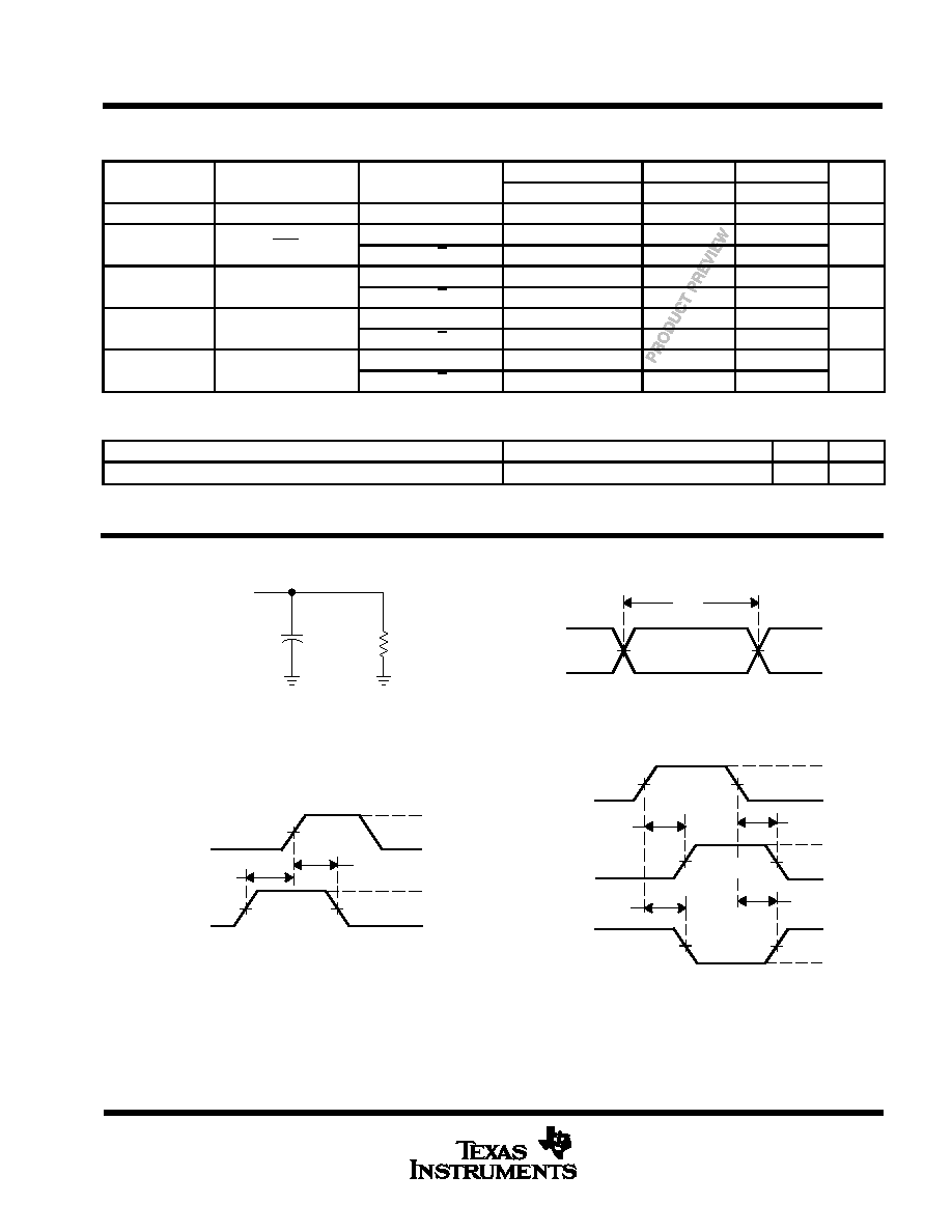
PARAMETER MEASUREMENT INFORMATION
50% VCC
50%
50%
50%
VCC
VCC
0 V
0 V
th
tsu
VOLTAGE WAVEFORMS
Data Input
tPLH
tPHL
tPHL
tPLH
VOH
VOH
VOL
VOL
50%
50%
VCC
0 V
50% VCC
50% VCC
Input
(see Note B)
Out-of-Phase
Output
In-Phase
Output
Timing Input
(see Note B)
50% VCC
VOLTAGE WAVEFORMS
VCC
0 V
50%
50%
tw
VOLTAGE WAVEFORMS
Input
LOAD CIRCUIT
From Output
Under Test
CL = 50 pF
(see Note A)
500
NOTES: A. CL includes probe and jig capacitance.
B. All input pulses are supplied by generators having the following characteristics: PRR
10 MHz, ZO = 50
, tr = 3 ns, tf = 3 ns.
C. The outputs are measured one at a time with one input transition per measurement.
Figure 1. Load Circuit and Voltage Waveforms
PRODUCT PREVIEW information concerns products in the formative or
design phase of development. Characteristic data and other
specifications are design goals. Texas Instruments reserves the right to
change or discontinue these products without notice.