 | –≠–ª–µ–∫—Ç—Ä–æ–Ω–Ω—ã–π –∫–æ–º–ø–æ–Ω–µ–Ω—Ç: 54AC11238 | –°–∫–∞—á–∞—Ç—å:  PDF PDF  ZIP ZIP |

54AC11238, 74AC11238
3-LINE TO 8-LINE DECODERS/DEMULTIPLEXERS
SCAS039A ≠ APRIL 1988 ≠ REVISED APRIL 1993
POST OFFICE BOX 655303
∑
DALLAS, TEXAS 75265
Copyright
©
1993, Texas Instruments Incorporated
2≠1
∑
Designed Specifically for High-Speed
Memory Decoders and Data Transmission
Systems
∑
Noninverting Version of
AC11138
∑
Incorporates 3 Enable Inputs to Simplify
Cascading and/or Data Reception
∑
Flow-Through Architecture Optimizes
PCB Layout
∑
Center-Pin V
CC
and GND Configurations
Minimize High-Speed Switching Noise
∑
EPIC
t
(Enhanced-Performance Implanted
CMOS) 1-
m
m Process
∑
500-mA Typical Latch-Up Immunity
at 125
∞
C
∑
Package Options Include Plastic
Small-Outline Packages, Ceramic Chip
Carriers, and Standard Plastic and Ceramic
300-mil DIPs
description
The
AC11238 circuit is designed to be
used in high-performance memory-decoding or
data-routing applications requiring very short
propagation delay times. In high-performance
memory systems, this decoder can be used to
minimize the effects of system decoding. When
employed with high-speed memories utilizing a
fast enable circuit, the delay times of this decoder
and the enable time of the memory are usually less than the typical access time of the memory. This means that
the effective system delay introduced by the decoder is negligible.
The conditions at the binary select inputs and the three enable inputs select one of eight input lines. Two
active-low and one active-high enable inputs reduce the need for external gates or inverters when expanding.
A 24-line decoder can be implemented without external inverters and a 32-line decoder requires only one
inverter. An enable input can be used as a data input for demultiplexing applications.
The 54AC11238 is characterized for operation over the full military temperature range of ≠ 55
∞
C to 125
∞
C. The
74AC11238 is characterized for operation from ≠ 40
∞
C to 85
∞
C.
PRODUCTION DATA information is current as of publication date.
Products conform to specifications per the terms of Texas Instruments
standard warranty. Production processing does not necessarily
include testing of all parameters.
54AC11238 . . . J PACKAGE
74AC11238 . . . D OR N PACKAGE
(TOP VIEW)
1
2
3
4
5
6
7
8
16
15
14
13
12
11
10
9
Y1
Y2
Y3
GND
Y4
Y5
Y6
Y7
Y0
A
B
C
V
CC
G1
G2A
G2B
3
2
1 20 19
9 10 11 12 13
4
5
6
7
8
18
17
16
15
14
A
Y0
NC
Y1
Y2
54AC11238 . . . FK PACKAGE
(TOP VIEW)
B
Y4
G1
GND
NC
CC
V
NC
Y5
Y3
NC ≠ No internal connection
C
G2A
G2B
NC
Y7
Y6
EPIC is a trademark of Texas Instruments Incorporated.
54AC11238, 74AC11238
3-LINE TO 8-LINE DECODERS/DEMULTIPLEXERS
SCAS039A ≠ APRIL 1988 ≠ REVISED APRIL 1993
POST OFFICE BOX 655303
∑
DALLAS, TEXAS 75265
2≠2
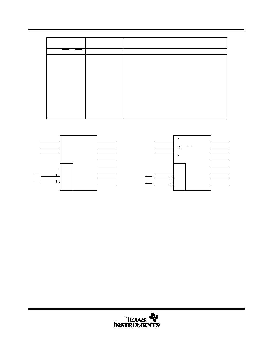
FUNCTION TABLE
ENABLE
INPUTS
SELECT
INPUTS
OUTPUTS
G1
G2A
G2B
C
B
A
Y0
Y1
Y2
Y3
Y4
Y5
Y6
Y7
X
H
X
X
X
X
L
L
L
L
L
L
L
L
X
X
H
X
X
X
L
L
L
L
L
L
L
L
L
X
X
X
X
X
L
L
L
L
L
L
L
L
H
L
L
L
L
L
H
L
L
L
L
L
L
L
H
L
L
L
L
H
L
H
L
L
L
L
L
L
H
L
L
L
H
L
L
L
H
L
L
L
L
L
H
L
L
L
H
H
L
L
L
H
L
L
L
L
H
L
L
H
L
L
L
L
L
L
H
L
L
L
H
L
L
H
L
H
L
L
L
L
L
H
L
L
H
L
L
H
H
L
L
L
L
L
L
L
H
L
H
L
L
H
H
H
L
L
L
L
L
L
L
H
logic symbols
(alternatives)
DMUX
0
2
G
0
7
A
B
C
G1
G2A
Y0
Y1
Y2
Y3
Y5
Y6
Y7
G2B
15
14
13
11
10
9
16
1
2
3
6
7
8
BIN/OCT
1
2
A
B
C
G1
G2A
Y0
Y1
Y2
Y3
Y5
Y6
Y7
G3A
15
14
13
11
10
9
16
1
2
3
6
7
8
4
0
1
2
3
0
1
2
3
Y4
5
4
Y4
5
4
5
6
7
&
EN
&
5
6
7
EN
These symbols are in accordance with ANSI/IEEE Std 91-1984 and IEC Publication 617-12.
54AC11238, 74AC11238
3-LINE TO 8-LINE DECODERS/DEMULTIPLEXERS
SCAS039A ≠ APRIL 1988 ≠ REVISED APRIL 1993
POST OFFICE BOX 655303
∑
DALLAS, TEXAS 75265
2≠3
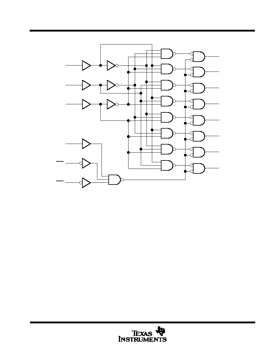
logic diagram (positive logic)
Y0
A
15
16
Y1
1
Y2
2
Y3
3
Y4
5
Y5
6
Y6
7
Y7
8
B
14
C
13
G1
11
G2A
10
G3A
9
Pin numbers shown are for the D, J, and N packages.
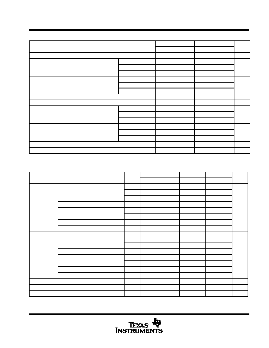
absolute maximum ratings over operating free-air temperature range (unless otherwise noted)
Supply voltage range, V
CC
≠ 0.5 V to 7 V
. . . . . . . . . . . . . . . . . . . . . . . . . . . . . . . . . . . . . . . . . . . . . . . . . . . . . . . . . .
Input voltage range, V
I
(see Note 1)
≠ 0.5 V to V
CC
+ 0.5 V
. . . . . . . . . . . . . . . . . . . . . . . . . . . . . . . . . . . . . . . . . . .
Output voltage range, V
O
(see Note 1)
≠ 0.5 V to V
CC
+ 0.5 V
. . . . . . . . . . . . . . . . . . . . . . . . . . . . . . . . . . . . . . . .
Input clamp current, I
IK
(V
I
< 0 or V
I
> V
CC
)
±
20 mA
. . . . . . . . . . . . . . . . . . . . . . . . . . . . . . . . . . . . . . . . . . . . . . . . .
Output clamp current, I
OK
(V
O
< 0 or V
O
> V
CC
)
±
50 mA
. . . . . . . . . . . . . . . . . . . . . . . . . . . . . . . . . . . . . . . . . . . .
Continuous output current, I
O
(V
O
= 0 to V
CC
)
±
50 mA
. . . . . . . . . . . . . . . . . . . . . . . . . . . . . . . . . . . . . . . . . . . . . .
Continuous current through V
CC
or GND
±
200 mA
. . . . . . . . . . . . . . . . . . . . . . . . . . . . . . . . . . . . . . . . . . . . . . . . . .
Storage temperature range
≠ 65
∞
C to 150
∞
C
. . . . . . . . . . . . . . . . . . . . . . . . . . . . . . . . . . . . . . . . . . . . . . . . . . . . . . . .
Stresses beyond those listed under "absolute maximum ratings" may cause permanent damage to the device. These are stress ratings only and
functional operation of the device at these or any other conditions beyond those indicated under "recommended operating conditions" is not
implied. Exposure to absolute-maximum-rated conditions for extended periods may affect device reliability.
NOTE 1: The input and output voltage ratings may be exceeded if the input and output current ratings are observed.
54AC11238, 74AC11238
3-LINE TO 8-LINE DECODERS/DEMULTIPLEXERS
SCAS039A ≠ APRIL 1988 ≠ REVISED APRIL 1993
POST OFFICE BOX 655303
∑
DALLAS, TEXAS 75265
2≠4
recommended operating conditions
54AC11238
74AC11238
UNIT
MIN
NOM
MAX
MIN
NOM
MAX
UNIT
VCC
Supply voltage
3
5
5.5
3
5
5.5
V
VCC = 3 V
2.1
2.1
VIH
High-level input voltage
VCC = 4.5 V
3.15
3.15
V
VCC = 5.5 V
3.85
3.85
VCC = 3 V
0.9
0.9
VIL
Low-level input voltage
VCC = 4.5 V
1.35
1.35
V
VCC = 5.5 V
1.65
1.65
VI
Input voltage
0
VCC
0
VCC
V
VO
Output voltage
0
VCC
0
VCC
V
VCC = 3 V
≠ 4
≠ 4
IOH
High-level output current
VCC = 4.5 V
≠ 24
≠ 24
mA
VCC = 5.5 V
≠ 24
≠ 24
VCC = 3 V
12
12
IOL
Low-level output current
VCC = 4.5 V
24
24
mA
VCC = 5.5 V
24
24
D
t /
D
v
Input transition rise or fall rate
0
10
0
10
ns/ V
TA
Operating free-air temperature
≠ 55
125
≠ 40
85
∞
C
electrical characteristics over recommended operating free-air temperature range (unless
otherwise noted)
PARAMETER
TEST CONDITIONS
VCC
TA = 25
∞
C
54AC11238
74AC11238
UNIT
PARAMETER
TEST CONDITIONS
VCC
MIN
TYP
MAX
MIN
MAX
MIN
MAX
UNIT
3 V
2.9
2.9
2.9
IOH = ≠ 50
m
A
4.5 V
4.4
4.4
4.4
5.5 V
5.4
5.4
5.4
VOH
IOH = ≠ 4 mA
3 V
2.58
2.4
2.48
V
VOH
IOH = 24 mA
4.5 V
3.94
3.7
3.8
V
IOH = ≠ 24 mA
5.5 V
4.94
4.7
4.8
IOH = ≠ 50 mA
}
5.5 V
3.85
IOH = ≠ 75 mA
}
5.5 V
3.85
3 V
0.1
0.1
0.1
IOL = 50
m
A
4.5 V
0.1
0.1
0.1
5.5 V
0.1
0.1
0.1
VOL
IOL = 12 mA
3 V
0.36
0.5
0.44
V
VOL
IOL = 24 mA
4.5 V
0.36
0.5
0.44
V
IOL = 24 mA
5.5 V
0.36
0.5
0.44
IOL = 50 mA
}
5.5 V
1.65
IOL = 75 mA
}
5.5 V
1.65
II
VI = VCC or GND
5.5 V
±
0.1
±
1
±
1
m
A
ICC
VI = VCC or GND, IO = 0
5.5 V
4
80
40
m
A
Ci
VI = VCC or GND
5 V
3.5
pF
All typical values are at VCC = 5 V, TA = 25
∞
C.
Not more than one output should be tested at a time, and the duration of the test should not exceed 10 ms.
54AC11238, 74AC11238
3-LINE TO 8-LINE DECODERS/DEMULTIPLEXERS
SCAS039A ≠ APRIL 1988 ≠ REVISED APRIL 1993
POST OFFICE BOX 655303
∑
DALLAS, TEXAS 75265
2≠5
switching characteristics over recommended operating free-air temperature range,
V
CC
= 3.3 V
±
0.3 V (unless otherwise noted) (see Figure 1)
PARAMETER
FROM
TO
TA = 25
∞
C
54AC11238
74AC11238
UNIT
PARAMETER
(INPUT)
(OUTPUT)
MIN
TYP
MAX
MIN
MAX
MIN
MAX
UNIT
tPLH
A B C
Any Y
1.5
8.5
10.6
1.5
12.7
1.5
11.7
ns
tPHL
A, B, C
Any Y
1.5
9.6
11.9
1.5
14.3
1.5
13.3
ns
tPLH
G1
Any Y
1.5
8.2
10.3
1.5
12.3
1.5
11.4
ns
tPHL
G1
Any Y
1.5
9.6
11.7
1.5
14
1.5
13
ns
tPLH
G2A G2B
Any Y
1.5
9.1
11.2
1.5
13.4
1.5
12.5
ns
tPHL
G2A, G2B
Any Y
1.5
10.7
12.9
1.5
15.6
1.5
14.5
ns
switching characteristics over recommended operating free-air temperature range,
V
CC
= 5 V
±
0.5 V (unless otherwise noted) (see Figure 1)
PARAMETER
FROM
TO
TA = 25
∞
C
54AC11238
74AC11238
UNIT
PARAMETER
(INPUT)
(OUTPUT)
MIN
TYP
MAX
MIN
MAX
MIN
MAX
UNIT
tPLH
A B C
Any Y
1.5
5.4
7.3
1.5
9
1.5
8.5
ns
tPHL
A, B, C
Any Y
1.5
6.3
8.6
1.5
10.9
1.5
10.2
ns
tPLH
G1
Any Y
1.5
5.2
6.9
1.5
8.7
1.5
8.1
ns
tPHL
G1
Any Y
1.5
6.5
8.5
1.5
10.6
1.5
9.9
ns
tPLH
G2A G2B
Any Y
1.5
5.6
7.5
1.5
9.6
1.5
8.9
ns
tPHL
G2A, G2B
Any Y
1.5
7.2
9.3
2.5
11.8
1.5
11
ns
operating characteristics, V
CC
= 5 V, T
A
= 25
∞
C
PARAMETER
TEST CONDITIONS
TYP
UNIT
Cpd Power dissipation capacitance
CL = 50 pF, f = 1 MHz
44
pF
PARAMETER MEASUREMENT INFORMATION
VOLTAGE WAVEFORMS
LOAD CIRCUIT
Input
(see Note B)
50%
50%
50% VCC
50% VCC
tPHL
tPLH
VCC
Output
VOL
VOH
0 V
From Output
Under Test
CL = 50 pF
(see Note A)
500
NOTES: A. CL includes probe and jig capacitance.
B. Input pulses are supplied by generators having the following characteristics: PRR
10 MHz, ZO = 50
, tr = 3 ns, tf = 3 ns.
C. The outputs are measured one at a time with one input transition per measurement.
Figure 1. Load Circuit and Voltage Waveforms