 | –≠–ª–µ–∫—Ç—Ä–æ–Ω–Ω—ã–π –∫–æ–º–ø–æ–Ω–µ–Ω—Ç: 54AC11534 | –°–∫–∞—á–∞—Ç—å:  PDF PDF  ZIP ZIP |
54AC11534, 74AC11534
OCTAL D-TYPE EDGE-TRIGGERED FLIP-FLOPS
WITH 3-STATE OUTPUTS
SCAS037A ≠ JULY 1987 ≠ REVISED APRIL 1993
POST OFFICE BOX 655303
∑
DALLAS, TEXAS 75265
Copyright
©
1993, Texas Instruments Incorporated
2≠1
∑
Eight D-Type Flip-Flops in a Single Package
∑
3-State Bus Driving Inverting Outputs
∑
Full Parallel Access for Loading
∑
Inputs Are TTL-Voltage Compatible
∑
Flow-Through Architecture to Optimize
PCB Layout
∑
Center-Pin V
CC
and GND Configurations to
Minimize High-Speed Switching Noise
∑
EPIC
t
(Enhanced-Performance Implanted
CMOS) 1-
m
m Process
∑
500-mA Typical Latch-Up Immunity
at 125
∞
C
∑
Package Options Include Plastic Small-
Outline Packages, Ceramic Chip Carriers,
and Standard Plastic and Ceramic 300-mil
DIPs
description
These eight flip-flops feature 3-state outputs
designed for implementing buffer registers, I/O
ports, bidirectional bus drivers, and working
registers.
The eight flip-flops of the
AC11534 are edge-
triggered, D-type flip-flops. On the positive
transition of the clock, the Q outputs are set to the
complement of the logic levels at the D inputs. The
AC11534 is functionally equivalent to the
AC11374 except for having inverted outputs.
An output-control input (OC) is used to place the
eight outputs in either a normal logic state (high or
low logic levels) or a high-impedance state. In the
high-impedance state, the outputs neither load
nor drive the bus lines significantly. The
high-impedance third state and increased drive
provide the capability to drive the bus lines in a
bus-organized system without need for interface
or pull-up components. The output control (OC)
does not affect the internal operation of the
flip-flops. Old data can be retained or new data
can be entered while the outputs are in the
high-impedance state.
The 54AC11534 is characterized for operation
over the full military temperature range of ≠ 55
∞
C
to 125
∞
C. The 74AC11534 is characterized for
operation from ≠ 40
∞
C to 85
∞
C.
1
2
3
4
5
6
7
8
9
10
11
12
24
23
22
21
20
19
18
17
16
15
14
13
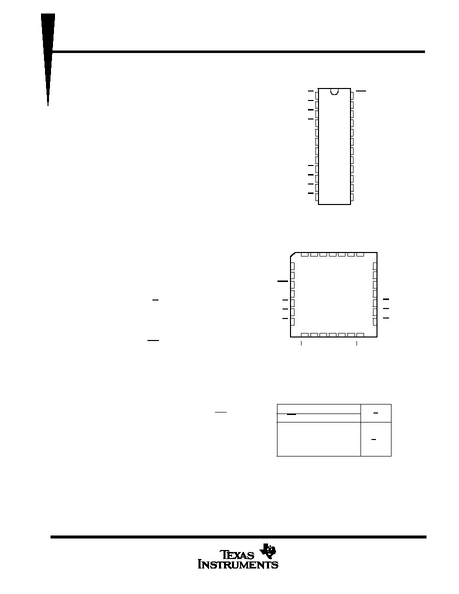
1Q
2Q
3Q
4Q
GND
GND
GND
GND
5Q
6Q
7Q
8Q
OC
1D
2D
3D
4D
V
CC
V
CC
5D
6D
7D
8D
CLK
54AC11534 . . . JT PACKAGE
74AC11534 . . . DW OR NT PACKAGE
(TOP VIEW)
3 2 1
13 14
5
6
7
8
9
10
11
7D
8D
CLK
NC
8Q
7Q
6Q
2D
1D
OC
NC
1Q
2Q
3Q
4
15 16 17 18
GND
GND
NC
GND
GND
5Q
3D
4D
NC
54AC11534 . . . FK PACKAGE
(TOP VIEW)
28 27 26
25
24
23
22
21
20
19
12
4Q
5D
6D
CC
V
CC
V
INPUTS
OUTPUT
Q
L
L
L
H
FUNCTION TABLE
(each filp-flop)
OC
CLK
D
L
X
H
L
X
X
L
H
Q0
Z
NC ≠ No internal connection
PRODUCTION DATA information is current as of publication date.
Products conform to specifications per the terms of Texas Instruments
standard warranty. Production processing does not necessarily include
testing of all parameters.
EPIC is a trademark of Texas Instruments Incorporated.
54AC11534, 74AC11534
OCTAL D-TYPE EDGE-TRIGGERED FLIP-FLOPS
WITH 3-STATE OUTPUTS
SCAS037A ≠ JULY 1987 ≠ REVISED APRIL 1993
POST OFFICE BOX 655303
∑
DALLAS, TEXAS 75265
2≠2
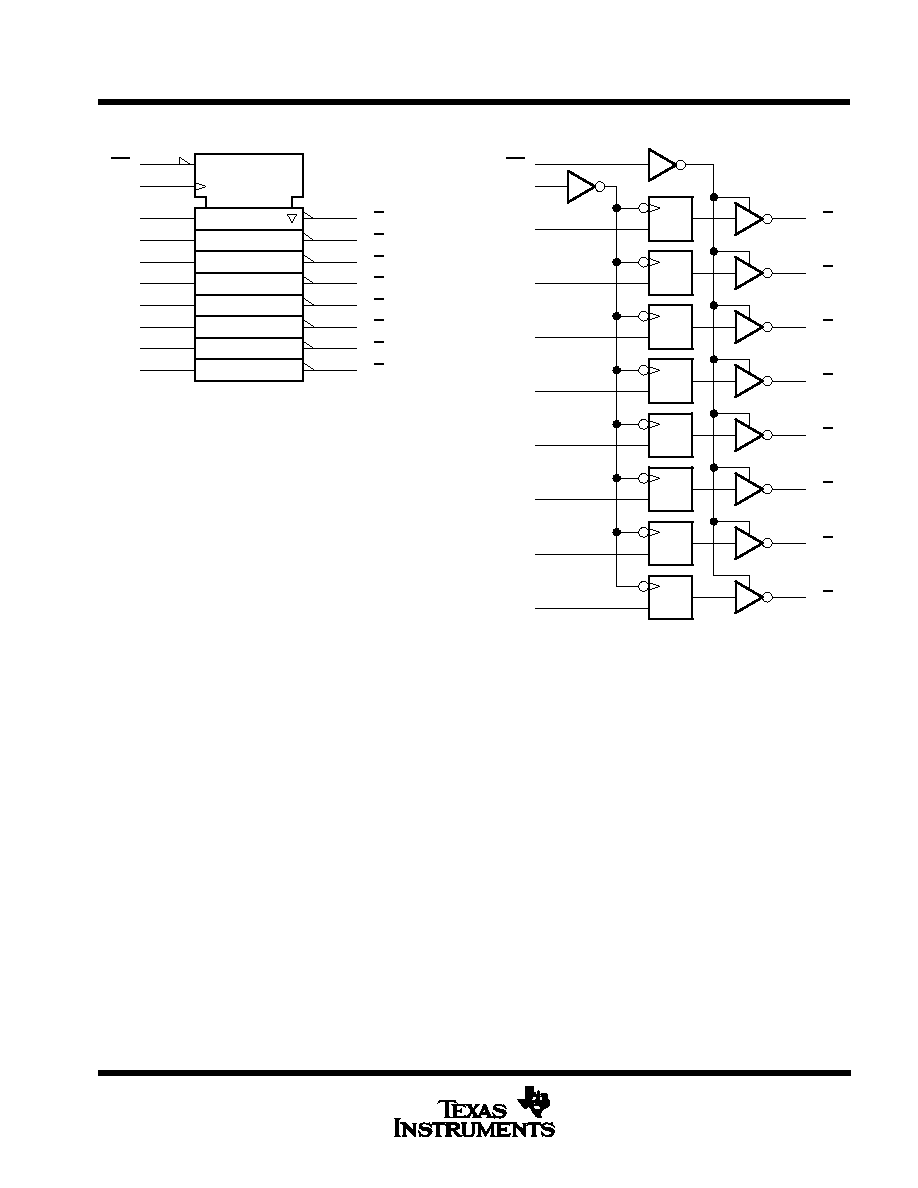
logic symbol
logic diagram (positive logic)
8D
7D
6D
5D
4D
3D
2D
1D
CLK
OC
14
15
16
17
20
21
22
23
13
24
1D
C1
EN
8Q
7Q
6Q
5Q
4Q
3Q
2Q
1Q
12
11
10
9
4
3
2
1
8D
7D
6D
5D
4D
3D
2D
1D
CLK
OC
14
15
16
17
20
21
22
23
13
24
8Q
7Q
6Q
5Q
4Q
3Q
2Q
1Q
12
11
10
9
4
3
2
1
C1
1D
1D
C1
C1
1D
1D
C1
C1
1D
1D
C1
C1
1D
1D
C1
This symbol is in accordance with ANSI/IEEE Std 91-1984
and IEC Publication 617-12.
Pin numbers shown are for the DW, JT, and NT packages.
absolute maximum ratings over operating free-air temperature range (unless otherwise noted)
Supply voltage range, V
CC
≠ 0.5 V to 7 V
. . . . . . . . . . . . . . . . . . . . . . . . . . . . . . . . . . . . . . . . . . . . . . . . . . . . . . . . . .
Input voltage range, V
I
(see Note 1)
≠ 0.5 V to V
CC
+ 0.5 V
. . . . . . . . . . . . . . . . . . . . . . . . . . . . . . . . . . . . . . . . . . .
Output voltage range, V
O
(see Note 1)
≠ 0.5 V to V
CC
+ 0.5 V
. . . . . . . . . . . . . . . . . . . . . . . . . . . . . . . . . . . . . . . .
Input clamp current, I
IK
(V
I
< 0 or V
I
> V
CC
)
±
20 mA
. . . . . . . . . . . . . . . . . . . . . . . . . . . . . . . . . . . . . . . . . . . . . . . . .
Output clamp current, I
OK
(V
O
< 0 or V
O
> V
CC
)
±
50 mA
. . . . . . . . . . . . . . . . . . . . . . . . . . . . . . . . . . . . . . . . . . . .
Continuous output current, I
O
(V
O
= 0 to V
CC
)
±
50 mA
. . . . . . . . . . . . . . . . . . . . . . . . . . . . . . . . . . . . . . . . . . . . . .
Continuous current through V
CC
or GND
±
200 mA
. . . . . . . . . . . . . . . . . . . . . . . . . . . . . . . . . . . . . . . . . . . . . . . . . .
Storage temperature range
≠ 65
∞
C to 150
∞
C
. . . . . . . . . . . . . . . . . . . . . . . . . . . . . . . . . . . . . . . . . . . . . . . . . . . . . . . .
Stresses beyond those listed under "absolute maximum ratings" may cause permanent damage to the device. These are stress ratings only and
functional operation of the device at these or any other conditions beyond those indicated under "recommended operating conditions" is not
implied. Exposure to absolute-maximum-rated conditions for extended periods may affect device reliability.
NOTE 1: The input and output voltage ratings may be exceeded if the input and output current ratings are observed.
54AC11534, 74AC11534
OCTAL D-TYPE EDGE-TRIGGERED FLIP-FLOPS
WITH 3-STATE OUTPUTS
SCAS037A ≠ JULY 1987 ≠ REVISED APRIL 1993
POST OFFICE BOX 655303
∑
DALLAS, TEXAS 75265
2≠3
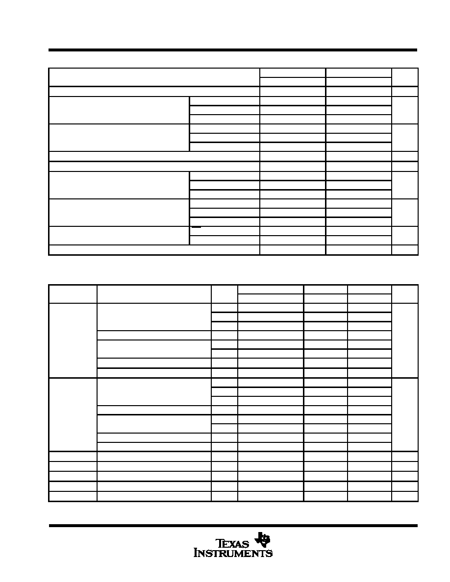
recommended operating conditions
54AC11534
74AC11534
UNIT
MIN
NOM
MAX
MIN
NOM
MAX
UNIT
VCC
Supply voltage
3
5
5.5
3
5
5.5
V
VCC = 3 V
2.1
2.1
VIH
High-level input voltage
VCC = 4.5 V
3.15
3.15
V
VCC = 5.5 V
3.85
3.85
VCC = 3 V
0.9
0.9
VIL
Low-level input voltage
VCC = 4.5 V
1.35
1.35
V
VCC = 5.5 V
1.65
1.65
VI
Input voltage
0
VCC
0
VCC
V
VO
Output voltage
0
VCC
0
VCC
V
VCC = 3 V
≠ 4
≠ 4
IOH
High-level output current
VCC = 4.5 V
≠ 24
≠ 24
mA
VCC = 5.5 V
≠ 24
≠ 24
VCC = 3 V
12
12
IOL
Low-level output current
VCC = 4.5 V
24
24
mA
VCC = 5.5 V
24
24
D
t /
D
v
Input transition rise or fall rate
OC
0
5
0
5
ns/ V
D
t /
D
v
Input transition rise or fall rate
D
0
10
0
10
ns/ V
TA
Operating free-air temperature
≠ 55
125
≠ 40
85
∞
C
electrical characteristics over recommended operating free-air temperature range (unless
otherwise noted)
PARAMETER
TEST CONDITIONS
VCC
TA = 25
∞
C
54AC11534
74AC11534
UNIT
PARAMETER
TEST CONDITIONS
VCC
MIN
TYP
MAX
MIN
MAX
MIN
MAX
UNIT
3 V
2.9
2.9
2.9
IOH = ≠ 50
m
A
4.5 V
4.4
4.4
4.4
5.5 V
5.4
5.4
5.4
V
IOH = ≠ 4 mA
3 V
2.58
2.4
2.48
V
VOH
IOH = 24 mA
4.5 V
3.94
3.7
3.8
V
IOH = ≠ 24 mA
5.5 V
4.94
4.7
4.8
IOH = ≠ 50 mA
{
5.5 V
3.85
IOH = ≠ 75 mA
{
5.5 V
3.85
3 V
0.1
0.1
0.1
IOL = 50
m
A
4.5 V
0.1
0.1
0.1
5.5 V
0.1
0.1
0.1
VOL
IOL = 12 mA
3 V
0.36
0.5
0.44
V
VOL
IOL = 24 mA
4.5 V
0.36
0.5
0.44
V
IOL = 24 mA
5.5 V
0.36
0.5
0.44
IOL = 50 mA
{
5.5 V
1.65
IOL = 75 mA
{
5.5 V
1.65
IOZ
VO = VCC or GND
5.5 V
±
0.5
±
10
±
5
m
A
II
VI = VCC or GND
5.5 V
±
0.1
±
1
±
1
m
A
ICC
VI = VCC or GND, IO = 0
5.5 V
8
160
80
m
A
Ci
VI = VCC or GND
5 V
4
pF
Co
VO = VCC or GND
5 V
10
pF
Not more than one output should be tested at a time, and the duration of the test should not exceed 10 ms.

54AC11534, 74AC11534
OCTAL D-TYPE EDGE-TRIGGERED FLIP-FLOPS
WITH 3-STATE OUTPUTS
SCAS037A ≠ JULY 1987 ≠ REVISED APRIL 1993
POST OFFICE BOX 655303
∑
DALLAS, TEXAS 75265
2≠4
timing requirements, V
CC
= 3.3 V
±
0.3 V (see Figure 1)
TA = 25
∞
C
54AC11534
74AC11534
UNIT
MIN
MAX
MIN
MAX
MIN
MAX
UNIT
fclock
Clock frequency
0
50
0
50
0
50
MHz
tw
Pulse duration, CLK low or CLK high
10
10
10
ns
tsu
Setup time, data before CLK
3.5
3.5
3.5
ns
th
Hold time, data after CLK
5.5
5.5
5.5
ns
timing requirements, V
CC
= 5 V
±
0.5 V (see Figure 1)
TA = 25
∞
C
54AC11534
74AC11534
UNIT
MIN
MAX
MIN
MAX
MIN
MAX
UNIT
fclock
Clock frequency
0
75
0
75
0
75
MHz
tw
Pulse duration, CLK low or CLK high
6.5
6.5
6.5
ns
tsu
Setup time, data before CLK
3.5
3.5
3.5
ns
th
Hold time, data after CLK
4.5
4.5
4.5
ns
switching characteristics over recommended operating free-air temperature range,
V
CC
= 3.3 V
±
0.3 V (unless otherwise noted) (see Figure 1)
PARAMETER
FROM
TO
TA = 25
∞
C
54AC11534
74AC11534
UNIT
PARAMETER
(INPUT)
(OUTPUT)
MIN
TYP
MAX
MIN
MAX
MIN
MAX
UNIT
fmax
50
75
50
50
MHz
tPLH
CLK
Q
1.5
11
15.3
1.5
19.1
1.5
17.6
ns
tPHL
CLK
Q
1.5
11
15.7
1.5
19
1.5
17.7
ns
tPZH
OC
Q
1.5
9
12.8
1.5
15.8
1.5
14.6
ns
tPZL
OC
Q
1.5
9
12.6
1.5
15.6
1.5
14.3
ns
tPHZ
OC
Q
1.5
10
12.6
1.5
13.8
1.5
13.3
ns
tPLZ
OC
Q
1.5
8
13
1.5
14.2
1.5
13.8
ns
switching characteristics over recommended operating free-air temperature range,
V
CC
= 5 V
±
0.5 V (unless otherwise noted) (see Figure 1)
PARAMETER
FROM
TO
TA = 25
∞
C
54AC11534
74AC11534
UNIT
PARAMETER
(INPUT)
(OUTPUT)
MIN
TYP
MAX
MIN
MAX
MIN
MAX
UNIT
fmax
75
100
75
75
MHz
tPLH
CLK
Q
1.5
7
10.3
1.5
12.7
1.5
11.7
ns
tPHL
CLK
Q
1.5
7
10.7
1.5
13.2
1.5
12.1
ns
tPZH
OC
Q
1.5
6
9.2
1.5
11.2
1.5
10.4
ns
tPZL
OC
Q
1.5
6
9.2
1.5
11.3
1.5
10.4
ns
tPHZ
OC
Q
1.5
9
11.1
1.5
11.9
1.5
11.6
ns
tPLZ
OC
Q
1.5
6
8.8
1.5
9.6
1.5
9.2
ns
operating characteristics, V
CC
= 5 V, T
A
= 25
∞
C
PARAMETER
TEST CONDITIONS
TYP
UNIT
C d
Power dissipation capacitance per flip flop
Outputs enabled
CL = 50 pF
f = 1 MHz
75
pF
Cpd Power dissipation capacitance per flip-flop
Outputs disabled
CL = 50 pF, f = 1 MHz
65
pF
54AC11534, 74AC11534
OCTAL D-TYPE EDGE-TRIGGERED FLIP-FLOPS
WITH 3-STATE OUTPUTS
SCAS037A ≠ JULY 1987 ≠ REVISED APRIL 1993
POST OFFICE BOX 655303
∑
DALLAS, TEXAS 75265
2≠5
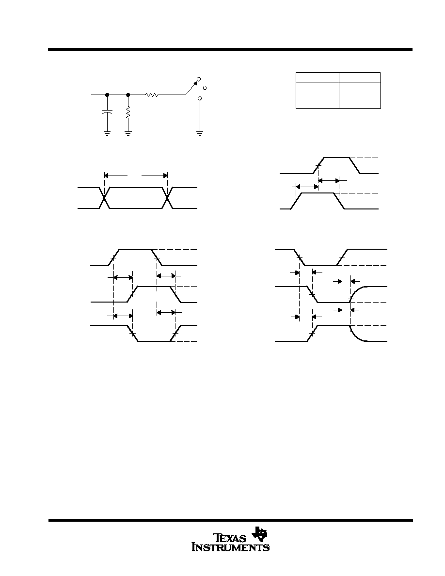
PARAMETER MEASUREMENT INFORMATION
50% VCC
50%
50%
50%
VCC
VCC
0 V
0 V
th
tsu
VOLTAGE WAVEFORMS
Data Input
tPLH
tPHL
tPHL
tPLH
VOH
VOH
VOL
VOL
50%
50%
VCC
0 V
50% VCC
50% VCC
Input
(see Note B)
Out-of-Phase
Output
In-Phase
Output
Timing Input
(see Note B)
50% VCC
VOLTAGE WAVEFORMS
From Output
Under Test
CL = 50 pF
(see Note A)
LOAD CIRCUIT
S1
2
◊
VCC
500
500
Output
Control
(low-level
enabling)
Output
Waveform 1
S1 at 2
◊
VCC
(see Note C)
Output
Waveform 2
S1 at GND
(see Note C)
VOL
VOH
tPZL
tPZH
tPLZ
tPHZ
50%
50%
[
VCC
0 V
50% VCC
20% VCC
50% VCC
80% VCC
[
0 V
VCC
GND
Open
VOLTAGE WAVEFORMS
tPLH/tPHL
tPLZ/tPZL
tPHZ/tPZH
Open
2
◊
VCC
GND
TEST
S1
VCC
0 V
50%
50%
tw
VOLTAGE WAVEFORMS
Input
NOTES: A. CL includes probe and jig capacitance.
B. All input pulses are supplied by generators having the following characteristics: PRR
10 MHz, ZO = 50
, tr = 3 ns, tf = 3 ns.
C. Waveform 1 is for an output with internal conditions such that the output is low except when disabled by the output control.
Waveform 2 is for an output with internal conditions such that the output is high except when disabled by the output control.
D. The outputs are measured one at a time with one input transition per measurement.
Figure 1. Load Circuit and Voltage Waveforms