Document Outline
- Features
- Table of Contents
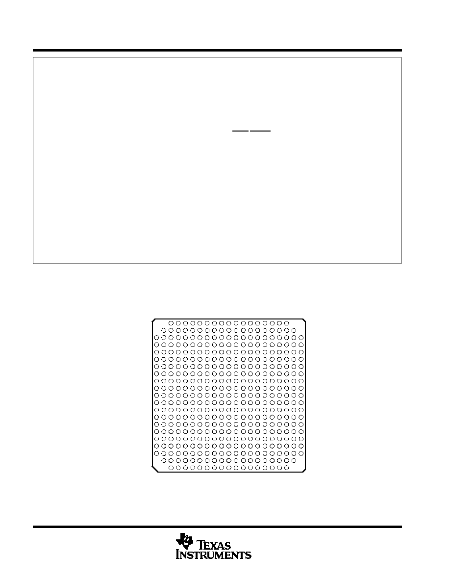
- GLP BGA package (bottom view)
- description
- device characteristics
- functional and CPU (DSP core) block diagram
- CPU (DSP core) description
- memory map summary
- peripheral register descriptions
- DMA synchronization events
- interrupt sources and interrupt selector
- signal groups description
- Signal Descriptions
- development support
- Software Development Tools:
- Hardware Development Tools:
- device and development-support tool nomenclature
- documentation support
- clock PLL
- power-supply sequencing
- system-level design considerations
- power-supply design considerations
- absolute maximum ratings over operating case temperature ranges (unless\
otherwise noted)
- recommended operating conditions
- electrical characteristics over recommended ranges of supply voltage and\
operating case temperature (unless otherwise noted)
- PARAMETER MEASUREMENT INFORMATION
- signal transition levels
- timing parameters and board routing analysis
- INPUT AND OUTPUT CLOCKS
- timing requirements for CLKIN (PLL used) (see Figure 11)
- timing requirements for CLKIN [PLL bypassed (x1)] (see Figure 11)
- timing requirements for XCLKIN (see Figure 12)
- switching characteristics over recommended operating conditions for CLKO\
UT2 (see Figure 13)
- switching characteristics over recommended operating conditions for XFCL\
K (see Figure 14)
- ASYNCHRONOUS MEMORY TIMING
- timing requirements for asynchronous memory cycles (see Figure 15 - Fig\
ure 18)
- switching characteristics over recommended operating conditions for asyn\
chronous memory cycles (see Figure 15-Figure 18)
- SYNCHRONOUS-BURST MEMORY TIMING
- timing requirements for synchronous-burst SRAM cycles (see Figure 19)
- switching characteristics over recommended operating conditions for sync\
hronous-burst SRAM cycles (see Figure 19 and Figure 2
- SYNCHRONOUS DRAM TIMING
- timing requirements for synchronous DRAM cycles (see Figure 21)
- switching characteristics over recommended operating conditions for sync\
hronous DRAM cycles for C6203B Rev.2 (see Figure 21-
- HOLD\/HOLDA\ TIMING
- timing requirements for the HOLD\/ HOLDA\ cycles (see Figure 27)
- switching characteristics over recommended operating conditions for the \
HOLD\/HOLDA\ cycles (see Figure 27)
- RESET TIMING
- timing requirements for reset (see Figure 28)
- switching characteristics over recommended operating conditions during r\
eset (see Figure 28)
- EXTERNAL INTERRUPT TIMING
- timing requirements for interrupt response cycles (see Figure 29)
- switching characteristics over recommended operating conditions during i\
nterrupt response cycles (see Figure 29)
- EXPANSION BUS SYNCHRONOUS FIFO TIMING
- timing requirements for synchronous FIFO interface (see Figure 30, Figu\
re 31, and Figure 32)
- switching characteristics over recommended operating conditions for sync\
hronous FIFO interface (see Figure 30, Figure 31, and
- EXPANSION BUS ASYNCHRONOUS PERIPHERAL TIMING
- timing requirements for asynchronous peripheral cycles (see Figure 33- \
Figure 36)
- switching characteristics over recommended operating conditions for asyn\
chronous peripheral cycles (see Figure 33- Figure 36)
- EXPANSION BUS SYNCHRONOUS HOST-PORT TIMING
- timing requirements with external device as bus master (see Figure 37 a\
nd Figure 38)
- switching characteristics over recommended operating conditions with ext\
ernal device as bus master (see Figure 37and Figure 3
- timing requirements with C62x as bus master (see Figure 39, Figure 40,\
and Figure 41)
- switching characteristics over recommended operating conditions with C62\
x as bus master (see Figure 39, Figure 40, and Fig
- EXPANSION BUS ASYNCHRONOUS HOST-PORT TIMING
- timing requirements with external device as asynchronous bus master (se\
e Figure 42 and Figure 43)
- switching characteristics over recommended operating conditions with ext\
ernal device as asynchronous bus master (see Figure 4
- XHOLD/XHOLDA TIMING
- timing requirements for expansion bus arbitration (internal arbiter ena\
bled) (see Figure 44)
- switching characteristics over recommended operating conditions for expa\
nsion bus arbitration (internal arbiter enabled) (see
- switching characteristics over recommended operating conditions for expa\
nsion bus arbitration (internal arbiter disabled)(see
- MULTICHANNEL BUFFERED SERIAL PORT TIMING
- timing requirements for McBSP (see Figure 46)
- switching characteristics over recommended operating conditions for McBS\
P (see Figure 46)
- timing requirements for FSR when GSYNC = 1 (see Figure 47)
- timing requirements for McBSP as SPI master or slave: CLKSTP = 10b, CLKX\
P = 0 (see Figure 48)
- switching characteristics over recommended operating conditions for McBS\
P as SPI master or slave: CLKSTP=10b, CLKXP = 0 (see
- timing requirements for McBSP as SPI master or slave: CLKSTP = 11b, CLKX\
P = 0 (see Figure 49)
- switching characteristics over recommended operating conditions for McBS\
P as SPI master or slave:CLKSTP =11b, CLKXP = 0 (see
- timing requirements for McBSP as SPI master or slave: CLKSTP = 10b, CLKX\
P = 1 (see Figure 50)
- switching characteristics over recommended operating conditions for McBS\
P as SPI master or slave: CLKSTP = 10b, CLKXP = 1(see
- timing requirements for McBSP as SPI master or slave: CLKSTP = 11b, CLKX\
P = 1 (see Figure 51)
- switching characteristics over recommended operating conditions for McBS\
P as SPI master or slave:CLKSTP = 11b, CLKXP =1 (see
- DMAC, TIMER, POWER-DOWN TIMING
- switching characteristics over recommended operating conditions for DMAC\
outputs (see Figure 52)
- timing requirements for timer inputs (see Figure 53)
- switching characteristics over recommended operating conditions for time\
r outputs (see Figure 53)
- switching characteristics over recommended operating conditions for powe\
r-down outputs (see Figure 54)
- JTAG TEST-PORT TIMING
- timing requirements for JTAG test port (see Figure 55)
- switching characteristics over recommended operating conditions for JTAG\
test port (see Figure 55)
- MECHANICAL DATA
- GLP (S-CBGA-N429) CERAMIC BALL GRID ARRAY
- thermal resistance characteristics (S-CBGA package)

SMJ320C6203
FIXED POINT DIGITAL SIGNAL PROCESSOR
SGUS033 � FEBRUARY 2002
1
POST OFFICE BOX 1443
�
HOUSTON, TEXAS 77251�1443
D
High-Performance Fixed-Point Digital
Signal Processor (DSP) � SMJ320C62x
� 5-ns Instruction Cycle Time
� 200-MHz Clock Rate
� Eight 32-Bit Instructions/Cycle
� 1600 Million Instructions Per Second
(MIPS)
D
429-Pin Ball Grid Array (BGA) Package
(GLP Suffix)
D
VelociTI
Advanced Very-Long-Instruction-
Word (VLIW) C62x
DSP Core
� Eight Highly Independent Functional
Units:
� Six Arithmetic Logic Units (ALUs)
(32-/40-Bit)
� Two 16-Bit Multipliers (32-Bit Result)
� Load-Store Architecture With 32 32-Bit
General-Purpose Registers
� Instruction Packing Reduces Code Size
� All Instructions Conditional
D
Instruction Set Features
� Byte-Addressable (8-, 16-, 32-Bit Data)
� 8-Bit Overflow Protection
� Saturation
� Bit-Field Extract, Set, Clear
� Bit-Counting
� Normalization
D
7M-Bit On-Chip SRAM
� 3M-Bit Internal Program/Cache
(96K 32-Bit Instructions)
� 4M-Bit Dual-Access Internal Data
(512K Bytes)
� Organized as Two 256K-Byte Blocks
for Improved Concurrency
D
Flexible Phase-Locked-Loop (PLL) Clock
Generator
D
32-Bit External Memory Interface (EMIF)
� Glueless Interface to Synchronous
Memories: SDRAM or SBSRAM
� Glueless Interface to Asynchronous
Memories: SRAM and EPROM
� 52M-Byte Addressable External Memory
Space
D
Four-Channel Bootloading
Direct-Memory-Access (DMA) Controller
With an Auxiliary Channel
D
32-Bit Expansion Bus
� Glueless/Low-Glue Interface to Popular
PCI Bridge Chips
� Glueless/Low-Glue Interface to Popular
Synchronous or Asynchronous
Microprocessor Buses
� Master/Slave Functionality
� Glueless Interface to Synchronous FIFOs
and Asynchronous Peripherals
D
Three Multichannel Buffered Serial Ports
(McBSPs)
� Direct Interface to T1/E1, MVIP, SCSA
Framers
� ST-Bus-Switching Compatible
� Up to 256 Channels Each
� AC97-Compatible
� Serial-Peripheral Interface (SPI)
Compatible (Motorola
)
D
Two 32-Bit General-Purpose Timers
D
IEEE-1149.1 (JTAG
)
Boundary-Scan-Compatible
D
0.15-
�
m/5-Level Metal Process
� CMOS Technology
D
3.3-V I/Os, 1.5-V Internal
PRODUCTION DATA information is current as of publication date.
Products conform to specifications per the terms of Texas Instruments
standard warranty. Production processing does not necessarily include
testing of all parameters.
Please be aware that an important notice concerning availability, standard warranty, and use in critical applications of
Texas Instruments semiconductor products and disclaimers thereto appears at the end of this data sheet.
SMJ320C62x, VelociTI, and C62x are trademarks of Texas Instruments.
Motorola is a trademark of Motorola, Inc.
All trademarks are the property of their respective owners.
IEEE Standard 1149.1-1990 Standard-Test-Access Port and Boundary Scan Architecture.
Copyright
2002, Texas Instruments Incorporated
On products compliant to MIL PRF 38535, all parameters are tested
unless otherwise noted. On all other products, production
processing does not necessarily include testing of all parameters.
SMJ320C6203
FIXED POINT DIGITAL SIGNAL PROCESSOR
SGUS033 � FEBRUARY 2002
2
POST OFFICE BOX 1443
�
HOUSTON, TEXAS 77251�1443
Table of Contents
signal transition levels
38
. . . . . . . . . . . . . . . . . . . . . . . . . .
timing parameters and board routing analysis
39
. . . . . .
input and output clocks
40
. . . . . . . . . . . . . . . . . . . . . . . . . . .
asynchronous memory timing
42
. . . . . . . . . . . . . . . . . . . . .
synchronous-burst memory timing
46
. . . . . . . . . . . . . . . . .
synchronous DRAM timing
48
. . . . . . . . . . . . . . . . . . . . . . . .
HOLD/HOLDA timing
52
. . . . . . . . . . . . . . . . . . . . . . . . . . . .
reset timing
52
. . . . . . . . . . . . . . . . . . . . . . . . . . . . . . . . . . . . .
external interrupt timing
54
. . . . . . . . . . . . . . . . . . . . . . . . . .
expansion bus synchronous FIFO timing
55
. . . . . . . . . . . .
expansion bus asynchronous peripheral timing
57
. . . . . .
expansion bus synchronous host-port timing
61
. . . . . . . .
expansion bus asynchronous host-port timing
67
. . . . . . .
XHOLD/XHOLDA timing
69
. . . . . . . . . . . . . . . . . . . . . . . . . .
multichannel buffered serial port timing
70
. . . . . . . . . . . . .
DMAC, timer, power-down timing
77
. . . . . . . . . . . . . . . . . .
JTAG test-port timing
78
. . . . . . . . . . . . . . . . . . . . . . . . . . . .
mechanical data
79
. . . . . . . . . . . . . . . . . . . . . . . . . . . . . . . . .
GLP BGA package (bottom view)
2
. . . . . . . . . . . . . . . . . . . .
description
3
. . . . . . . . . . . . . . . . . . . . . . . . . . . . . . . . . . . . . . .
device characteristics
3
. . . . . . . . . . . . . . . . . . . . . . . . . . . . . .
functional and CPU (DSP core) block diagram
5
. . . . . . . . .
CPU (DSP core) description
6
. . . . . . . . . . . . . . . . . . . . . . . .
memory map summary
8
. . . . . . . . . . . . . . . . . . . . . . . . . . . . .
peripheral register descriptions
9
. . . . . . . . . . . . . . . . . . . . . .
DMA synchronization events
14
. . . . . . . . . . . . . . . . . . . . . . .
interrupt sources and interrupt selector
15
. . . . . . . . . . . . . .
signal groups description
16
. . . . . . . . . . . . . . . . . . . . . . . . . .
signal descriptions
19
. . . . . . . . . . . . . . . . . . . . . . . . . . . . . . . .
development support
31
. . . . . . . . . . . . . . . . . . . . . . . . . . . . . .
documentation support
33
. . . . . . . . . . . . . . . . . . . . . . . . . . . .
clock PLL
34
. . . . . . . . . . . . . . . . . . . . . . . . . . . . . . . . . . . . . . .
power-supply sequencing
36
. . . . . . . . . . . . . . . . . . . . . . . . . .
absolute maximum ratings over operating case
temperature ranges
37
. . . . . . . . . . . . . . . . . . . . . . . . . . . .
recommended operating conditions
37
. . . . . . . . . . . . . . . . .
electrical characteristics over recommended ranges
of supply voltage and operating case temperature
37
. .
parameter measurement information
38
. . . . . . . . . . . . . . . .
GLP BGA package (bottom view)
GLP 429-PIN BALL GRID ARRAY (BGA) PACKAGE (BOTTOM VIEW)
20
21
19
18
16
15
17
13
11
10
12
14
W
Y
AA
V
T
U
P
M
N
R
8
7
6
4
5
L
J
K
G
E
F
H
3
2
D
B
C
A
1
9

SMJ320C6203
FIXED POINT DIGITAL SIGNAL PROCESSOR
SGUS033 � FEBRUARY 2002
3
POST OFFICE BOX 1443
�
HOUSTON, TEXAS 77251�1443
description
The SMJ320C6203 device is part of the SMJ320C62x
fixed-point DSP generation in the SMJ320C6000
DSP platform. The C62x
DSP devices are based on the high-performance, advanced VelociTI
very-long-instruction-word (VLIW) architecture developed by Texas Instruments (TI), making these DSPs an
excellent choice for multichannel and multifunction applications.
The SMJ320C62x
DSP offers cost-effective solutions to high-performance DSP-programming challenges.
The SMJ320C6203 has a performance capability of up to 1600 MIPS at a clock rate of 200 MHz. The C6203
DSP possesses the operational flexibility of high-speed controllers and the numerical capability of array
processors. This processor has 32 general-purpose registers of 32-bit word length and eight highly
independent functional units. The eight functional units provide six arithmetic logic units (ALUs) for a high
degree of parallelism and two 16-bit multipliers for a 32-bit result. The C6203 can produce two
multiply-accumulates (MACs) per cycle for a total of 400 million MACs per second (MMACS). The C6203 DSP
also has application-specific hardware logic, on-chip memory, and additional on-chip peripherals.
The C6203 device program memory consists of two blocks, with a 256K-byte block configured as
memory-mapped program space, and the other 128K-byte block user-configurable as cache or
memory-mapped program space. Data memory for the C6203 consists of two 256K-byte blocks of RAM.
The C6203 device has a powerful and diverse set of peripherals. The peripheral set includes three multichannel
buffered serial ports (McBSPs), two general-purpose timers, a 32-bit expansion bus that offers ease of interface
to synchronous or asynchronous industry-standard host bus protocols, and a glueless 32-bit external memory
interface (EMIF) capable of interfacing to SDRAM or SBSRAM and asynchronous peripherals.
The C62x
devices have a complete set of development tools that includes: a new C compiler, an assembly
optimizer to simplify programming and scheduling, and a Windows
debugger interface for visibility into source
code execution.
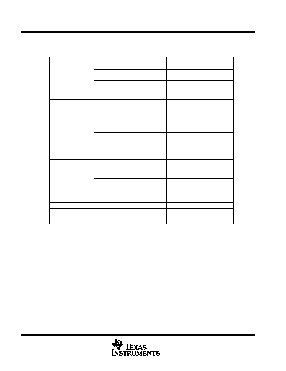
device characteristics
Table 1 provides an overview of the SMJ320C6203 DSP. The table shows significant features of the device,
including the capacity of on-chip RAM, the peripherals, the execution time, and the package type with pin count.
This data sheet focuses on the functionality of the SMJ320C6203 device. For more details on the C6000
DSP
part numbering, see Figure 4.
SMJ320C6000 and C6000 are trademarks of Texas Instruments.
Windows is a registered trademark of the Microsoft Corporation.
SMJ320C6203
FIXED POINT DIGITAL SIGNAL PROCESSOR
SGUS033 � FEBRUARY 2002
4
POST OFFICE BOX 1443
�
HOUSTON, TEXAS 77251�1443
device characteristics (continued)
Table 1. Characteristics of the C6203 DSP
HARDWARE FEATURES
C6203
EMIF
P i h
l
DMA
4-Channel With Throughput
Enhancements
Peripherals
Expansion Bus
McBSPs
3
32-Bit Timers
2
Size (Bytes)
384K
Internal Program
Memory
Organization
Block 0:
256K-Byte Mapped Program
Block 1:
128K-Byte Cache/Mapped Program
Size (Bytes)
512K
Internal Data Memory
Organization
2 Blocks:
Four 16-Bit Banks per Block
50/50 Split
CPU ID +
CPU Rev ID
Control Status Register (CSR.[31:16])
0x0003
Frequency
MHz
200
Cycle Time
ns
5 ns (6203-200)
Voltage
Core (V)
1.5
Voltage
I/O (V)
3.3
PLL Options
CLKIN frequency multiplier [Bypass (x1),
x4, x6, x7, x8, x9, x10, and x11]
Bypass (x1), x4, x6, x7,
x8, x9, x10, and x11
BGA Package
27 x 27 mm
GLP
Process Technology
�
m
0.15
�
m
Product Status
Product Preview (PP)
Advance Information (AI)
Production Data (PD)
PD
SMJ320C6203
FIXED POINT DIGITAL SIGNAL PROCESSOR
SGUS033 � FEBRUARY 2002
5
POST OFFICE BOX 1443
�
HOUSTON, TEXAS 77251�1443
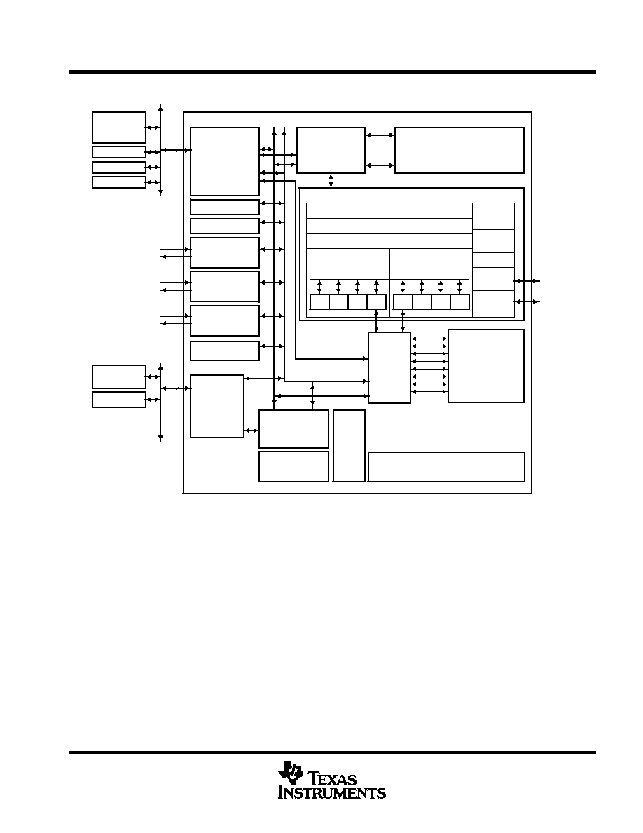
functional and CPU (DSP core) block diagram
32
Multichannel
Buffered Serial
Port 1
32
Direct Memory
Access Controller
(DMA)
(See Table 1)
Test
C62x CPU (DSP Core)
Data Path B
B Register File
Program
Access/Cache
Controller
Instruction Fetch
Instruction Dispatch
Instruction Decode
Data Path A
A Register File
PLL
(x1, x4, x6, x7, x8,
x9, x10, x11, x12)
Data
Access
Controller
Power-
Down
Logic
.L1
.S1
.M1
.D1
.D2 .M2
.S2
.L2
SDRAM or
SBSRAM
ROM/FLASH
SRAM
I/O Devices
Synchronous
FIFOs
I/O Devices
Timer 0
Timer 1
External Memory
Interface (EMIF)
Multichannel
Buffered Serial
Port 0
Multichannel
Buffered Serial
Port 2
Expansion
Bus
32-Bit
Internal Program Memory
2 Blocks Program/Cache
(384K Bytes)
Control
Registers
Control
Logic
Internal Data
Memory
(512K Bytes)
In-Circuit
Emulation
Interrupt
Control
Framing Chips:
H.100, MVIP,
SCSA, T1, E1
AC97 Devices,
SPI Devices,
Codecs
HOST CONNECTION
Master /Slave
TI PCI2040
Power PC
683xx
960
C6203 Digital Signal Processors
Peripheral Control Bus
DMA
Bus
Boot Configuration
Interrupt
Selector
For additional details on the PLL clock module and specific options for the C6203 device, see Table 1 and the Clock PLL section of this data sheet.