Document Outline
- features
- applications
- description
- functional block diagram
- Terminal Functions
- absolute maximum ratings over operating free-air temperature (unless ot\
herwise noted)
- THERMAL CHARACTERISTICS
- recommended operating conditions
- electrical characteristics over recommended operating free-air temperatu\
re range, AVDD=DVDD=3.3V (unless otherwise noted)
- PARAMETER MEASUREMENT INFORMATION
- sample timing
- read timing (15-pF load)
- write timing (15-pF load)
- TYPICAL CHARACTERISTICS
- PRINCIPLES OF OPERATION
- APPLICATION INFORMATION
- driving the analog input
- fully differential configuration
- transformer coupled single-ended to differential configuration
- single-ended configuration
- AC-coupled single-ended configuration
- internal/external reference operation
- programmable gain amplifier
- out of range indication
- offset compensation
- test modes
- digital I/O
- MECHANICAL DATA
- PFB (S-PQFP-G48) PLASTIC QUAD FLATPACK
- PHP (S-PQFP-G48) PowerPAD PLASTIC QUAD FLATPACK
- IMPORTANT NOTICE

THS1401, THS1403, THS1408
14-BIT, 1/3/8 MSPS DSP COMPATIBLE ANALOG-TO-DIGITAL CONVERTERS
WITH INTERNAL REFERENCE AND PGA
SLAS248C ≠ DECEMBER 1999 ≠ REVISED JULY 2002
1
POST OFFICE BOX 655303
∑
DALLAS, TEXAS 75265
features
D
14-Bit Resolution
D
1, 3, and 8 MSPS Speed Grades Available
D
Differential Nonlinearity (DNL)
±
0.6 LSB Typ
D
Integral Nonlinearity (INL)
±
1.5 LSB Typ
D
Internal Reference
D
Differential Inputs
D
Programmable Gain Amplifier
D
µ
P Compatible Parallel Interface
D
Timing Compatible With TMS320C6000 DSP
D
3.3-V Single Supply
D
Power-Down Mode
D
Monolithic CMOS Design
applications
D
xDSL Front Ends
D
Communication
D
Industrial Control
D
Instrumentation
D
Automotive
14 15
WR
OE
DGND
DGND
CLK
DV
DD
DV
DD
D0
D1
D2
DV
DD
DGND
36
35
34
33
32
31
30
29
28
27
26
25
16
1
2
3
4
5
6
7
8
9
10
11
12
IN≠
AV
DD
VBG
CML
REF+
REF≠
AGND
AGND
DGND
OV
D13
D12
17 18 19 20
A0
A1
NC
NC
47 46 45 44 43
48
42
IN+
AV
AGND
AGND
AGND
D5
D4
D3
DGND
D9
D8
D7
D6
40 39 38
41
21 22 23 24
37
13
CS
D1
1
D10
PFB AND PHP PACKAGE
(TOP VIEW)
DD
AV
DD
DV
DD
DV
DD
DV
DD
NC ≠ No internal connection
Copyright
2002, Texas Instruments Incorporated
PRODUCTION DATA information is current as of publication date.
Products conform to specifications per the terms of Texas Instruments
standard warranty. Production processing does not necessarily include
testing of all parameters.
Please be aware that an important notice concerning availability, standard warranty, and use in critical applications of
Texas Instruments semiconductor products and disclaimers thereto appears at the end of this data sheet.
On products compliant to MIL-PRF-38535, all parameters are tested
unless otherwise noted. On all other products, production
processing does not necessarily include testing of all parameters.

THS1401, THS1403, THS1408
14-BIT, 1/3/8 MSPS DSP COMPATIBLE ANALOG-TO-DIGITAL CONVERTERS
WITH INTERNAL REFERENCE AND PGA
SLAS248C ≠ DECEMBER 1999 ≠ REVISED JULY 2002
2
POST OFFICE BOX 655303
∑
DALLAS, TEXAS 75265
description
The THS1401, THS1403, and THS1408 are 14-bit, 1/3/8 MSPS, single supply analog-to-digital converters with
an internal reference, differential inputs, programmable input gain, and an on-chip sample and hold amplifier.
Implemented with a CMOS process, the device has outstanding price/performance and power/speed ratios.
The THS1401, THS1403, and THS1408 are designed for use with 3.3-V systems, and with a high-speed
µ
P
compatible parallel interface, making them the first choice for solutions based on high-performance DSPs like
the TI TMS320C6000 series.
The THS1401, THS1403, and THS1408 are available in a TQFP-48 package in standard commercial and
industrial temperature ranges. The THS1401, THS1403, and THS1408 are available in a PQFP-48 package
in automotive temperature range, and the THS1408 is available in a PQFP-48 package in military temperature
range.
functional block diagram
PGA
0..7 dB
REF
14-Bit
ADC
Buffer
14
15
CONTROL
LOGIC
REF+
REF≠
IN+
IN≠
D[13:0] + OV bit
A[1:0]
6
CLK
1.5 V
BG
VBG
CS
WR
OE
AVAILABLE OPTIONS
PACKAGED DEVICE
TA
TQFP
(PFB)
PQFP (Power Pad)
(PHP)
0
∞
C to 70
∞
C
THS1401CPFB,
THS1403CPFB,
THS1408CPFB,
--
≠40
∞
C to 85
∞
C
THS1401IPFB,
THS1403IPFB,
THS1408IPFB
--
≠40
∞
C to 125
∞
C
--
THS1401QPHP,
THS1403QPHP,
THS1408QPHP
≠55
∞
C to 125
∞
C
--
THS1408MPHP
THS1401, THS1403, THS1408
14-BIT, 1/3/8 MSPS DSP COMPATIBLE ANALOG-TO-DIGITAL CONVERTERS
WITH INTERNAL REFERENCE AND PGA
SLAS248C ≠ DECEMBER 1999 ≠ REVISED JULY 2002
3
POST OFFICE BOX 655303
∑
DALLAS, TEXAS 75265
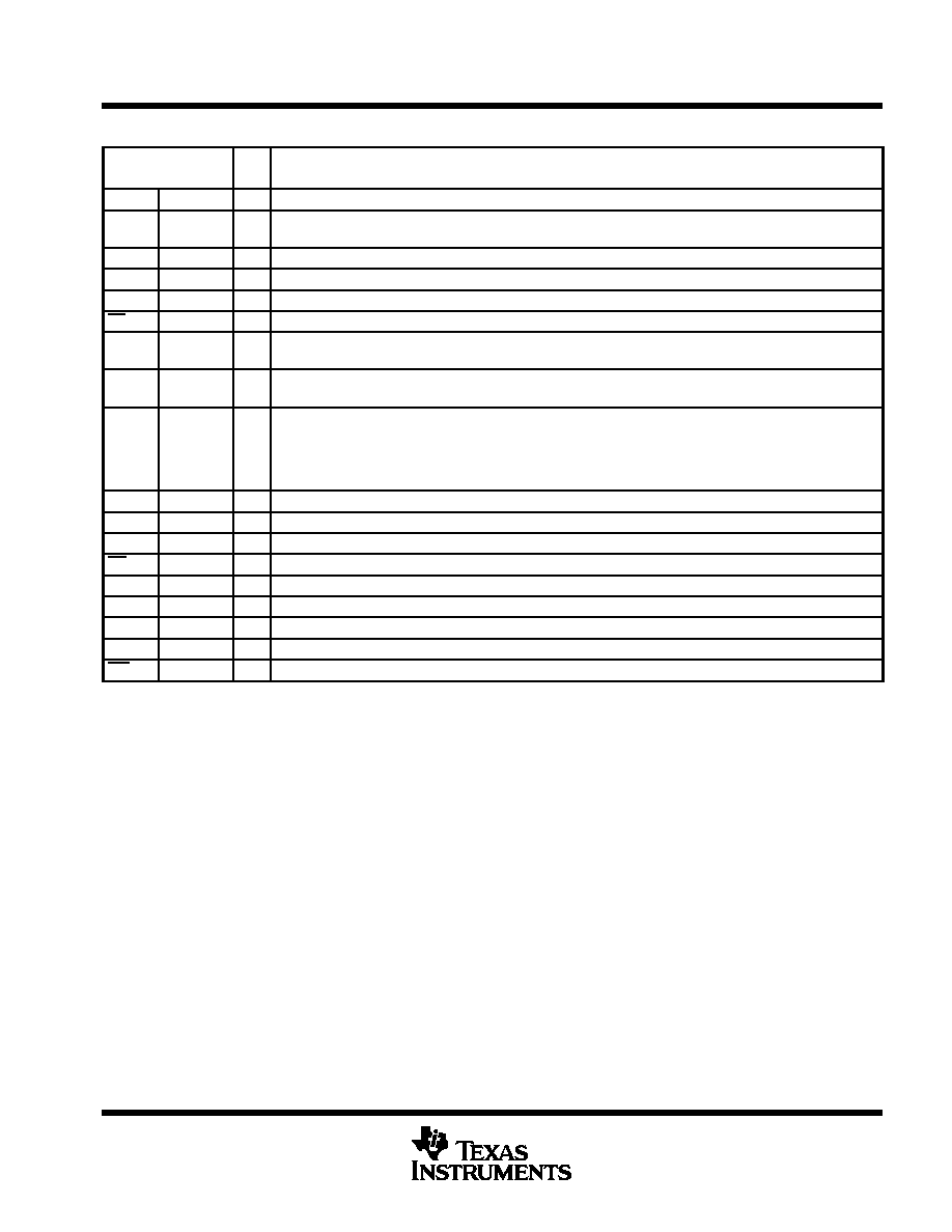
Terminal Functions
TERMINAL
I/O
DESCRIPTION
NAME
NO.
I/O
DESCRIPTION
A[1:0]
40, 41
I
Address input
AGND
7,8, 44,
45, 46
Analog ground
AVDD
2, 43, 47
Analog power supply
CLK
32
I
Clock input
CML
4
Reference midpoint. This pin requires a 0.1-
µ
F capacitor to AGND.
CS
37
I
Chip select input. Active low
DGND
9, 15, 25,
33, 34
Digital ground
DVDD
14, 20, 26,
30, 31, 42
Digital power supply
D[13:0]
11, 12, 13,
16, 17, 18,
19, 21, 22,
23, 24, 27,
28, 29
I/O
Data inputs/outputs
NC
38, 39
No connection, do not use. Reserved
IN+
48
I
Positive differential analog input
IN≠
1
I
Negative differential analog input
OE
35
I
Output enable. Active low
OV
10
O
Out of range output
REF+
5
O
Positive reference output. This pin requires a 0.1-
µ
F capacitor to AGND.
REF≠
6
O
Negative reference output. This pin requires a 0.1-
µ
F capacitor to AGND.
VBG
3
I
Reference input. This pin requires a 1-
µ
F capacitor to AGND.
WR
36
I
Write signal. Active low

THS1401, THS1403, THS1408
14-BIT, 1/3/8 MSPS DSP COMPATIBLE ANALOG-TO-DIGITAL CONVERTERS
WITH INTERNAL REFERENCE AND PGA
SLAS248C ≠ DECEMBER 1999 ≠ REVISED JULY 2002
4
POST OFFICE BOX 655303
∑
DALLAS, TEXAS 75265
absolute maximum ratings over operating free-air temperature (unless otherwise noted)
Supply voltage, (AV
DD
to AGND)
4V
. . . . . . . . . . . . . . . . . . . . . . . . . . . . . . . . . . . . . . . . . . . . . . . . . . . . . . . . . . . . .
Supply voltage, (DV
DD
to DGND)
4V
. . . . . . . . . . . . . . . . . . . . . . . . . . . . . . . . . . . . . . . . . . . . . . . . . . . . . . . . . . . . .
Reference input voltage range, VBG
≠ 0.3 V to AV
DD
+ 0.3 V
. . . . . . . . . . . . . . . . . . . . . . . . . . . . . . . . . . . . . . .
Analog input voltage range
≠ 0.3 V to AV
DD
+ 0.3 V
. . . . . . . . . . . . . . . . . . . . . . . . . . . . . . . . . . . . . . . . . . . . . . . . .
Digital input voltage range
≠ 0.3 V to DV
DD
+ 0.3 V
. . . . . . . . . . . . . . . . . . . . . . . . . . . . . . . . . . . . . . . . . . . . . . . . .
Operating free-air temperature range, T
A
: C
suffix
0
∞
C to 70
∞
C
. . . . . . . . . . . . . . . . . . . . . . . . . . . . . . . . . . . . . .
I suffix
≠40
∞
C to 85
∞
C
. . . . . . . . . . . . . . . . . . . . . . . . . . . . . . . . . . . . .
Q suffix
≠40
∞
C to 125
∞
C
. . . . . . . . . . . . . . . . . . . . . . . . . . . . . . . . . .
M suffix
≠55
∞
C to 125
∞
C
. . . . . . . . . . . . . . . . . . . . . . . . . . . . . . . . . .
Storage temperature range, T
stg
≠65
∞
C to 150
∞
C
. . . . . . . . . . . . . . . . . . . . . . . . . . . . . . . . . . . . . . . . . . . . . . . . . .
Lead temperature 1,6 mm (1/16 inch) from case for 10 seconds
260
∞
C
. . . . . . . . . . . . . . . . . . . . . . . . . . . . . . . .
Stresses beyond those listed under "absolute maximum ratings" may cause permanent damage to the device. These are stress ratings only, and
functional operation of the device at these or any other conditions beyond those indicated under "recommended operating conditions" is not
implied. Exposure to absolute-maximum-rated conditions for extended periods may affect device reliability.
THERMAL CHARACTERISTICS
TYP
UNIT
Thermal resistance junction to ambient
JA
PFB package
85.9
∞
C/W
Thermal resistance, junction-to-ambient,
JA
PHP package
28.8
∞
C/W
Thermal resistance junction to case
JC
PFB package
19.6
∞
C/W
Thermal resistance, junction-to-case,
JC
PHP package
0.79
∞
C/W
Thermal resistance is modeled data, is not production tested, and is given for informational purposes only.
recommended operating conditions
MIN
NOM
MAX
UNIT
Supply voltage, AVDD, DVDD
3
3.3
3.6
V
High level digital input, VIH
2
3.3
V
Low level digital input, VIL
0
0.8
V
Load capacitance, CL
5
15
pF
THS1401
0.1
1
1
MHz
Clock frequency, fCLK
THS1403
0.1
3
3
MHz
THS1408
0.1
8
8
MHz
Clock duty cycle
C and I suffix
40%
50%
60%
Clock duty cycle
Q and M suffix
45%
50%
55%
C suffix
0
25
70
Operating free air temperature
I suffix
≠40
25
85
∞
C
Operating free-air temperature
Q suffix
≠40
25
125
∞
C
M suffix
≠55
25
125

THS1401, THS1403, THS1408
14-BIT, 1/3/8 MSPS DSP COMPATIBLE ANALOG-TO-DIGITAL CONVERTERS
WITH INTERNAL REFERENCE AND PGA
SLAS248C ≠ DECEMBER 1999 ≠ REVISED JULY 2002
5
POST OFFICE BOX 655303
∑
DALLAS, TEXAS 75265
electrical characteristics over recommended operating free-air temperature range,
AV
DD
= DV
DD
= 3.3 V (unless otherwise noted)
PARAMETER
TEST CONDITIONS
MIN
TYP
MAX
UNIT
Power Supply
IDDA
Analog supply current
AVDD = 3.6 V
81
90
mA
IDDD
Digital supply current
DVDD = 3.6 V
5
10
mA
Power
AVDD = DVDD = 3.6 V
270
360
mW
Power down current
20
µ
A
DC Characteristics
Resolution
14
Bits
DNL
Differential nonlinearity
±
0.6
±
1
LSB
THS1401
±
1.5
±
2.5
THS1403C/I
±
1.5
±
2.5
INL
Integral nonlinearity
THS1403Q
Best fit
±
2
±
3
LSB
THS1408C/I
±
3
±
5
THS1408Q/M
±
3.5
±
7.5
Offset error
IN+ = IN≠, PGA = 0 dB
0.3
%FSR
Gain error
C and I suffix
PGA = 0 dB
1
%FSR
Gain error
Q and M suffix
PGA = 0 dB
1.75
%FSR
AC Characteristics
ENOB
Effective number of bits
11.2
11.5
Bits
THS1401/3/8
fi = 100 kHz
≠81
THD
Total harmonic distortion
THS1403/8
fi = 1 MHz
≠78
dB
THS1408
fi = 4 MHz
≠77
THS1401/3/8
fi = 100 kHz
72
SNR
Signal-to-noise ratio
THS1403/8
fi = 1 MHz
70
72
dB
THS1408
fi = 4 MHz
71
THS1401/3/8
fi = 100 kHz
70
SINAD
Signal-to-noise ratio + distortion
THS1403/8
fi = 1 MHz
69
70
dB
THS1408
fi = 4 MHz
70
THS1401/3/8
fi = 100 kHz
80
SFDR
Spurious free dynamic range
THS1403C/I, THS1408C/I
fi = 1 MHz
73
80
dB
SFDR
Spurious free dynamic range
THS1403Q, THS1408Q/M
fi = 1 MHz
71
80
dB
THS1408
fi = 4 MHz
80
Analog input bandwidth
140
MHz