
SN54LS240, SN54LS241, SN54LS244, SN54S240, SN54S241, SN54S244
SN74LS240, SN74LS241, SN74LS244, SN74S240, SN74S241, SN74S244
OCTAL BUFFERS AND LINE DRIVERS WITH 3-STATE OUTPUTS
SDLS144B ≠ APRIL 1985 ≠ REVISED FEBRUARY 2002
1
POST OFFICE BOX 655303
∑
DALLAS, TEXAS 75265
D
3-State Outputs Drive Bus Lines or Buffer
Memory Address Registers
D
PNP Inputs Reduce DC Loading
D
Hysteresis at Inputs Improves Noise
Margins
description
These octal buffers and line drivers are designed
specifically to improve both the performance and
density of three-state memory address drivers,
clock drivers, and bus-oriented receivers and
transmitters. The designer has a choice of
selected combinations of inverting and
noninverting outputs, symmetrical, active-low
output-control (G) inputs, and complementary
output-control (G and G) inputs. These devices
feature high fan-out, improved fan-in, and 400-mV
noise margin. The SN74LS' and SN74S' devices
can be used to drive terminated lines down to
133
.
Copyright
2002, Texas Instruments Incorporated
PRODUCTION DATA information is current as of publication date.
Products conform to specifications per the terms of Texas Instruments
standard warranty. Production processing does not necessarily include
testing of all parameters.
Please be aware that an important notice concerning availability, standard warranty, and use in critical applications of
Texas Instruments semiconductor products and disclaimers thereto appears at the end of this data sheet.
1
2
3
4
5
6
7
8
9
10
20
19
18
17
16
15
14
13
12
11
1G
1A1
2Y4
1A2
2Y3
1A3
2Y2
1A4
2Y1
GND
V
CC
2G/2G
1Y1
2A4
1Y2
2A3
1Y3
2A2
1Y4
2A1
SN54LS', SN54S' . . . J OR W PACKAGE
SN74LS240, SN74LS244 . . . DB, DW, N, OR NS PACKAGE
SN74LS241 . . . DW, N, OR NS PACKAGE
SN74S' . . . DW OR N PACKAGE
(TOP VIEW)
3
2
1 20 19
9 10 11 12 13
4
5
6
7
8
18
17
16
15
14
1Y1
2A4
1Y2
2A3
1Y3
1A2
2Y3
1A3
2Y2
1A4
SN54LS', SN54S' . . . FK PACKAGE
(TOP VIEW)
2Y4
1A1
1G
1Y4
2A2
2G/2G
2Y1
GND
2A1
V
CC
2G for 'LS241 and 'S241 or 2G for all other drivers.
2G for 'LS241 and 'S241 or 2G for all other drivers.
On products compliant to MIL-PRF-38535, all parameters are tested
unless otherwise noted. On all other products, production
processing does not necessarily include testing of all parameters.

SN54LS240, SN54LS241, SN54LS244, SN54S240, SN54S241, SN54S244
SN74LS240, SN74LS241, SN74LS244, SN74S240, SN74S241, SN74S244
OCTAL BUFFERS AND LINE DRIVERS WITH 3-STATE OUTPUTS
SDLS144B ≠ APRIL 1985 ≠ REVISED FEBRUARY 2002
2
POST OFFICE BOX 655303
∑
DALLAS, TEXAS 75265
ORDERING INFORMATION
TA
PACKAGE
ORDERABLE
PART NUMBER
TOP-SIDE
MARKING
SN74LS240N
SN74LS240N
SN74LS241N
SN74LS241N
PDIP
N
Tube
SN74LS244N
SN74LS244N
PDIP ≠ N
Tube
SN74S240N
SN74S240N
SN74S241N
SN74S241N
SN74S244N
SN74S244N
Tube
SN74LS240DW
LS240
Tape and reel
SN74LS240DWR
LS240
Tube
SN74LS241DW
LS241
Tape and reel
SN74LS241DWR
LS241
Tube
SN74LS244DW
LS244
0
∞
C to 70
∞
C
SOIC
DW
Tape and reel
SN74LS244DWR
LS244
SOIC ≠ DW
Tube
SN74S240DW
S240
Tape and reel
SN74S240DWR
S240
Tube
SN74S241DW
S241
Tape and reel
SN74S241DWR
S241
Tube
SN74S244DW
S244
Tape and reel
SN74S244DWR
S244
SN74LS240NSR
74LS240
SOP ≠ NS
Tube
SN74LS241NSR
74LS241
SN74LS244NSR
74LS244
SSOP
DB
Tape and reel
SN74LS240DBR
LS240
SSOP ≠ DB
Tape and reel
SN74LS244DBR
LS244
Package drawings, standard packing quantities, thermal data, symbolization, and PCB design guidelines are available at
www.ti.com/sc/package.

SN54LS240, SN54LS241, SN54LS244, SN54S240, SN54S241, SN54S244
SN74LS240, SN74LS241, SN74LS244, SN74S240, SN74S241, SN74S244
OCTAL BUFFERS AND LINE DRIVERS WITH 3-STATE OUTPUTS
SDLS144B ≠ APRIL 1985 ≠ REVISED FEBRUARY 2002
3
POST OFFICE BOX 655303
∑
DALLAS, TEXAS 75265
ORDERING INFORMATION (CONTINUED)
TA
PACKAGE
ORDERABLE
PART NUMBER
TOP-SIDE
MARKING
SN54LS240J
SN54LS240J
SNJ54LS240J
SNJ54LS240J
SN54LS241J
SN54LS241J
SNJ54LS241J
SNJ54LS241J
SN54LS244J
SN54LS244J
CDIP
J
Tube
SNJ54LS244J
SNJ54LS244J
CDIP ≠ J
Tube
SN54S240J
SN54S240J
SNJ54S240J
SNJ54S240J
SN54S241J
SN54S241J
SNJ54S241J
SNJ54S241J
SN54S244J
SN54S244J
55
∞
C to 125
∞
C
SNJ54S244J
SNJ54S244J
≠55
∞
C to 125
∞
C
SNJ54LS240W
SNJ54LS240W
SNJ54LS241W
SNJ54LS241W
CFP
W
Tube
SNJ54LS244W
SNJ54LS244W
CFP ≠ W
Tube
SNJ54S240W
SNJ54S240W
SNJ54S241W
SNJ54S241W
SNJ54S244W
SNJ54S244W
SNJ54LS240FK
SNJ54LS240FK
SNJ54LS241FK
SNJ54LS241FK
LCCC
FK
Tube
SNJ54LS244FK
SNJ54LS244FK
LCCC ≠ FK
Tube
SNJ54S240FK
SNJ54S240FK
SNJ54S241FK
SNJ54S241FK
SNJ54S244FK
SNJ54S244FK
Package drawings, standard packing quantities, thermal data, symbolization, and PCB design guidelines are available at
www.ti.com/sc/package.
SN54LS240, SN54LS241, SN54LS244, SN54S240, SN54S241, SN54S244
SN74LS240, SN74LS241, SN74LS244, SN74S240, SN74S241, SN74S244
OCTAL BUFFERS AND LINE DRIVERS WITH 3-STATE OUTPUTS
SDLS144B ≠ APRIL 1985 ≠ REVISED FEBRUARY 2002
4
POST OFFICE BOX 655303
∑
DALLAS, TEXAS 75265
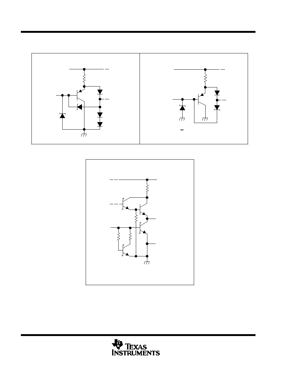
schematics of inputs and outputs
R
VCC
Output
TYPICAL OF ALL OUTPUTS
Req
VCC
Input
EQUIVALENT OF EACH INPUT
EQUIVALENT OF EACH INPUT
9 k
NOM
Input
VCC
'LS240. 'LS241, 'LS244: R = 50
NOM
'S240, `S241, S244: R = 25
NOM
GND
G and G inputs: Req = 2 k
NOM
A inputs: Req = 2.8 k
NOM
'LS240, 'LS241, 'LS244
'S240, 'S241, 'S244

SN54LS240, SN54LS241, SN54LS244, SN54S240, SN54S241, SN54S244
SN74LS240, SN74LS241, SN74LS244, SN74S240, SN74S241, SN74S244
OCTAL BUFFERS AND LINE DRIVERS WITH 3-STATE OUTPUTS
SDLS144B ≠ APRIL 1985 ≠ REVISED FEBRUARY 2002
5
POST OFFICE BOX 655303
∑
DALLAS, TEXAS 75265
logic diagram
1
2
4
6
8
19
11
13
15
17
3
5
7
9
12
14
16
18
1A1
1A2
1A3
1A4
1Y1
2A1
2A2
2A3
2A4
2Y1
1Y2
1Y3
1Y4
2Y2
2Y3
2Y4
2G
1G
'LS240, 'S240
'LS241, 'S241
'LS244, 'S244
1
2
4
6
8
19
11
13
15
17
3
5
7
9
12
14
16
18
1A1
1A2
1A3
1A4
1Y1
2A1
2A2
2A3
2A4
2Y1
1Y2
1Y3
1Y4
2Y2
2Y3
2Y4
2G
1G
1
2
4
6
8
19
11
13
15
17
3
5
7
9
12
14
16
18
1A1
1A2
1A3
1A4
1Y1
2A1
2A2
2A3
2A4
2Y1
1Y2
1Y3
1Y4
2Y2
2Y3
2Y4
2G
1G
Pin numbers shown are for DB, DW, J, N, NS, and W packages.