SN54ALS138A, SN54AS138, SN74ALS138A, SN74AS138
3-LINE TO 8-LINE DECODERS/DEMULTIPLEXERS
SDAS055E ≠ APRIL 1982 ≠ REVISED JULY 1996
1
POST OFFICE BOX 655303
∑
DALLAS, TEXAS 75265
D
Designed Specifically for High-Speed
Memory Decoders and Data Transmission
Systems
D
Incorporate Three Enable Inputs to Simplify
Cascading and /or Data Reception
D
Package Options Include Plastic
Small-Outline (D) Packages, Ceramic Chip
Carriers (FK), and Standard Plastic (N) and
Ceramic (J) 300-mil DIPs
description
The
ALS138A and
AS138 are 3-line to 8-line
decoders/demultiplexers designed for high-
performance memory-decoding or data-routing
applications requiring very short propagation
delay times. In high-performance systems, these
devices can be used to minimize the effects of
system decoding. When employed with
high-speed memories with a fast enable circuit,
the delay times of the decoder and the enable time
of the memory are usually less than the typical
access time of the memory. The effective system
delay introduced by the Schottky-clamped system
decoder is negligible.
The conditions at the binary-select (A, B, and C)
inputs and the three enable (G1, G2A, and G2B)
inputs select one of eight output lines. Two
active-low and one active-high enable inputs
reduce the need for external gates or inverters when expanding. A 24-line decoder can be implemented without
external inverters and a 32-line decoder requires only one inverter. An enable input can be used as a data input
for demultiplexing applications.
The SN54ALS138A and SN54AS138 are characterized for operation over the full military temperature range
of ≠ 55
∞
C to 125
∞
C. The SN74ALS138A and SN74AS138 are characterized for operation from 0
∞
C to 70
∞
C.
Copyright
©
1996, Texas Instruments Incorporated
PRODUCTION DATA information is current as of publication date.
Products conform to specifications per the terms of Texas Instruments
standard warranty. Production processing does not necessarily include
testing of all parameters.
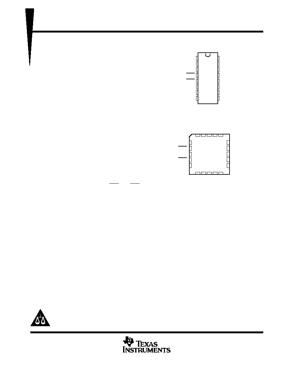
SN54ALS138A, SN54AS138 . . . J PACKAGE
SN74ALS138A, SN74AS138 . . . D OR N PACKAGE
(TOP VIEW)
3
2
1 20 19
9 10 11 12 13
4
5
6
7
8
18
17
16
15
14
Y1
Y2
NC
Y3
Y4
C
G2A
NC
G2B
G1
SN54ALS138A, SN54AS138 . . . FK PACKAGE
(TOP VIEW)
B
A
NC
Y6
Y5
Y0
Y7
GND
NC
NC ≠ No internal connection
V
CC
1
2
3
4
5
6
7
8
16
15
14
13
12
11
10
9
A
B
C
G2A
G2B
G1
Y7
GND
V
CC
Y0
Y1
Y2
Y3
Y4
Y5
Y6
Please be aware that an important notice concerning availability, standard warranty, and use in critical applications of
Texas Instruments semiconductor products and disclaimers thereto appears at the end of this data sheet.

SN54ALS138A, SN54AS138, SN74ALS138A, SN74AS138
3-LINE TO 8-LINE DECODERS/DEMULTIPLEXERS
SDAS055E ≠ APRIL 1982 ≠ REVISED JULY 1996
2
POST OFFICE BOX 655303
∑
DALLAS, TEXAS 75265
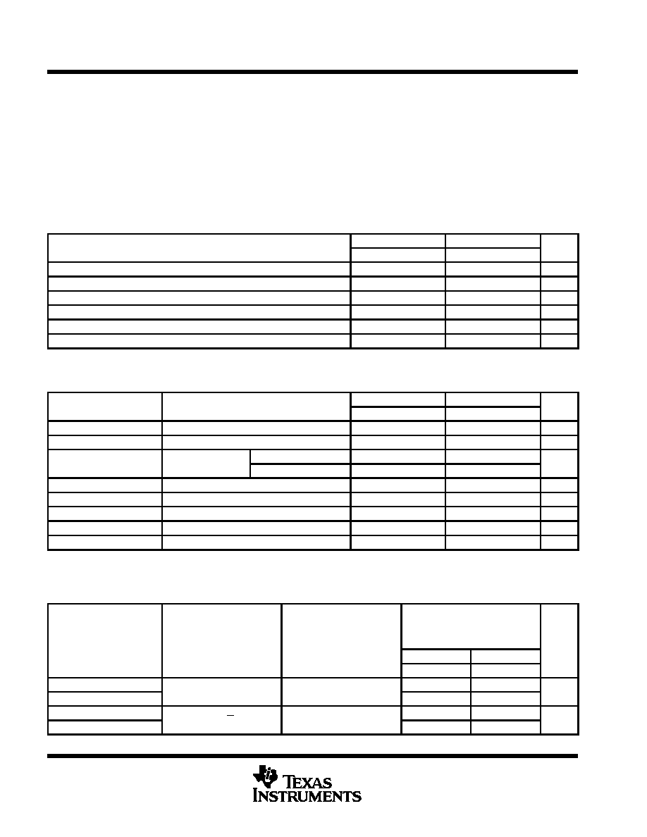
FUNCTION TABLE
INPUTS
OUTPUTS
ENABLE
SELECT
OUTPUTS
G1
G2A
G2B
C
B
A
Y0
Y1
Y2
Y3
Y4
Y5
Y6
Y7
X
H
X
X
X
X
H
H
H
H
H
H
H
H
X
X
H
X
X
X
H
H
H
H
H
H
H
H
L
X
X
X
X
X
H
H
H
H
H
H
H
H
H
L
L
L
L
L
L
H
H
H
H
H
H
H
H
L
L
L
L
H
H
L
H
H
H
H
H
H
H
L
L
L
H
L
H
H
L
H
H
H
H
H
H
L
L
L
H
H
H
H
H
L
H
H
H
H
H
L
L
H
L
L
H
H
H
H
L
H
H
H
H
L
L
H
L
H
H
H
H
H
H
L
H
H
H
L
L
H
H
L
H
H
H
H
H
H
L
H
H
L
L
H
H
H
H
H
H
H
H
H
H
L
logic symbols (alternatives)
BIN/OCT
1
1
A
2
2
B
4
3
C
4
5
6
G1
Y0
15
0
&
EN
Y1
14
1
Y2
13
2
Y3
12
3
Y4
11
4
Y5
10
5
Y6
9
6
Y7
7
7
DMUX
0
1
A
2
B
2
3
C
4
5
6
G1
Y0
15
0
&
Y1
14
1
Y2
13
2
Y3
12
3
Y4
11
4
Y5
10
5
Y6
9
6
Y7
7
7
G
7
0
G2A
G2B
G2A
G2B
These symbols are in accordance with ANSI/IEEE Std 91-1984 and IEC Publication 617-12.
Pin numbers shown are for the D, J, and N packages.

SN54ALS138A, SN54AS138, SN74ALS138A, SN74AS138
3-LINE TO 8-LINE DECODERS/DEMULTIPLEXERS
SDAS055E ≠ APRIL 1982 ≠ REVISED JULY 1996
3
POST OFFICE BOX 655303
∑
DALLAS, TEXAS 75265
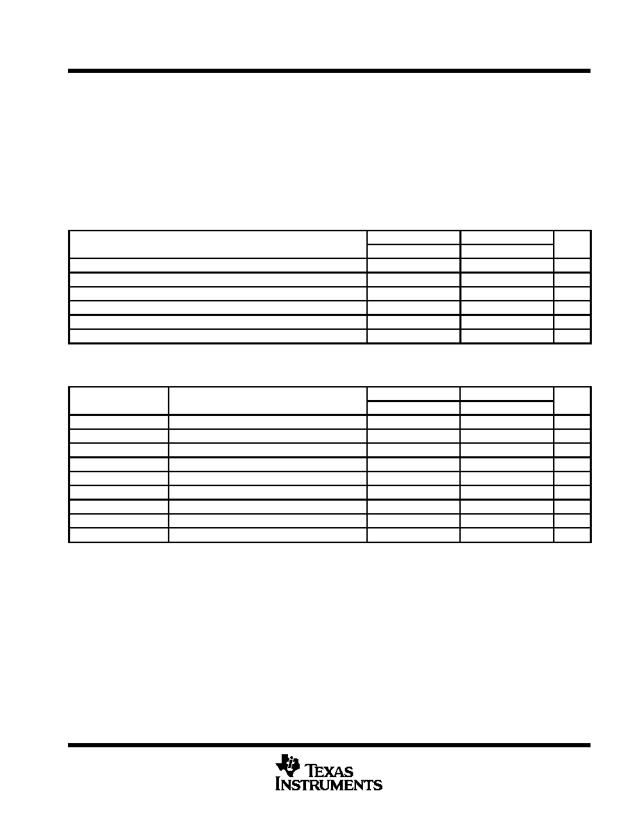
logic diagram (positive logic)
G2B
G2A
G1
C
B
A
Y7
Y6
Y5
Y4
Y3
Y2
Y1
Y0
Data
Outputs
Select
Inputs
Enable
Inputs
1
2
3
6
4
5
15
14
13
12
11
10
9
7
Pin numbers shown are for the D, J, and N packages.
SN54ALS138A, SN54AS138, SN74ALS138A, SN74AS138
3-LINE TO 8-LINE DECODERS/DEMULTIPLEXERS
SDAS055E ≠ APRIL 1982 ≠ REVISED JULY 1996
4
POST OFFICE BOX 655303
∑
DALLAS, TEXAS 75265
absolute maximum ratings over operating free-air temperature range (unless otherwise noted)
Supply voltage, V
CC
7 V
. . . . . . . . . . . . . . . . . . . . . . . . . . . . . . . . . . . . . . . . . . . . . . . . . . . . . . . . . . . . . . . . . . . . . . .
Input voltage, V
I
7 V
. . . . . . . . . . . . . . . . . . . . . . . . . . . . . . . . . . . . . . . . . . . . . . . . . . . . . . . . . . . . . . . . . . . . . . . . . . .
Operating free-air temperature range, T
A
: SN54ALS138A
≠ 55
∞
C to 125
∞
C
. . . . . . . . . . . . . . . . . . . . . . . . . . .
SN74ALS138A
0
∞
C to 70
∞
C
. . . . . . . . . . . . . . . . . . . . . . . . . . . . . . .
Storage temperature range, T
stg
≠ 65
∞
C to 150
∞
C
. . . . . . . . . . . . . . . . . . . . . . . . . . . . . . . . . . . . . . . . . . . . . . . . . .
Stresses beyond those listed under "absolute maximum ratings" may cause permanent damage to the device. These are stress ratings only, and
functional operation of the device at these or any other conditions beyond those indicated under "recommended operating conditions" is not
implied. Exposure to absolute-maximum-rated conditions for extended periods may affect device reliability.
recommended operating conditions
SN54ALS138A
SN74ALS138A
UNIT
MIN
NOM
MAX
MIN
NOM
MAX
UNIT
VCC
Supply voltage
4.5
5
5.5
4.5
5
5.5
V
VIH
High-level input voltage
2
2
V
VIL
Low-level input voltage
0.7
0.8
V
IOH
High-level output current
≠ 0.4
≠ 0.4
mA
IOL
Low-level output current
4
8
mA
TA
Operating free-air temperature
≠ 55
125
0
70
∞
C
electrical characteristics over recommended operating free-air temperature range (unless
otherwise noted)
PARAMETER
TEST CONDITIONS
SN54ALS138A
SN74ALS138A
UNIT
PARAMETER
TEST CONDITIONS
MIN
TYP
MAX
MIN
TYP
MAX
UNIT
VIK
VCC = 4.5 V,
II = ≠ 18 mA
≠ 1.5
≠ 1.5
V
VOH
VCC = 4.5 V,
IOH = ≠ 0.4 mA
VCC ≠ 2
VCC ≠ 2
V
VOL
VCC = 4 5 V
IOL = 4 mA
0.25
0.4
0.25
0.4
V
VOL
VCC = 4.5 V
IOL = 8 mA
0.35
0.5
V
II
VCC = 5.5 V,
VI = 7 V
0.1
0.1
mA
IIH
VCC = 5.5 V,
VI = 2.7 V
20
20
µ
A
IIL
VCC = 5.5 V,
VI = 0.4 V
≠ 0.1
≠ 0.1
mA
IOß
VCC = 5.5 V,
VO = 2.25 V
≠ 20
≠ 112
≠ 30
≠ 112
mA
ICC
VCC = 5.5 V
5
10
5
10
mA
All typical values are at VCC = 5 V, TA = 25
∞
C.
ß The output conditions have been chosen to produce a current that closely approximates one half of the true short-circuit output current, IOS.
switching characteristics (see Figure 1)
PARAMETER
FROM
(INPUT)
TO
(OUTPUT)
VCC = 4.5 V to 5.5 V,
CL = 50 pF,
RL = 500
,
TA = MIN to MAX∂
UNIT
(INPUT)
(OUTPUT)
SN54ALS138A
SN74ALS138A
MIN
MAX
MIN
MAX
tPLH
A B C
Any Y
2
28
5
22
ns
tPHL
A, B, C
Any Y
6
22
6
18
ns
tPLH
G or G
Any Y
2
22
3
17
ns
tPHL
G or G
Any Y
4
21
4
17
ns
∂ For conditions shown as MIN or MAX, use the appropriate value specified under recommended operating conditions.
SN54ALS138A, SN54AS138, SN74ALS138A, SN74AS138
3-LINE TO 8-LINE DECODERS/DEMULTIPLEXERS
SDAS055E ≠ APRIL 1982 ≠ REVISED JULY 1996
5
POST OFFICE BOX 655303
∑
DALLAS, TEXAS 75265
absolute maximum ratings over operating free-air temperature range (unless otherwise noted)
Supply voltage, V
CC
7 V
. . . . . . . . . . . . . . . . . . . . . . . . . . . . . . . . . . . . . . . . . . . . . . . . . . . . . . . . . . . . . . . . . . . . . . .
Input voltage, V
I
7 V
. . . . . . . . . . . . . . . . . . . . . . . . . . . . . . . . . . . . . . . . . . . . . . . . . . . . . . . . . . . . . . . . . . . . . . . . . . .
Operating free-air temperature range, T
A
: SN54AS138
≠ 55
∞
C to 125
∞
C
. . . . . . . . . . . . . . . . . . . . . . . . . . . . . .
SN74AS138
0
∞
C to 70
∞
C
. . . . . . . . . . . . . . . . . . . . . . . . . . . . . . . . . .
Storage temperature range, T
stg
≠ 65
∞
C to 150
∞
C
. . . . . . . . . . . . . . . . . . . . . . . . . . . . . . . . . . . . . . . . . . . . . . . . . .
Stresses beyond those listed under "absolute maximum ratings" may cause permanent damage to the device. These are stress ratings only, and
functional operation of the device at these or any other conditions beyond those indicated under "recommended operating conditions" is not
implied. Exposure to absolute-maximum-rated conditions for extended periods may affect device reliability.
recommended operating conditions
SN54AS138
SN74AS138
UNIT
MIN
NOM
MAX
MIN
NOM
MAX
UNIT
VCC
Supply voltage
4.5
5
5.5
4.5
5
5.5
V
VIH
High-level input voltage
2
2
V
VIL
Low-level input voltage
0.8
0.8
V
IOH
High-level output current
≠ 2
≠ 2
mA
IOL
Low-level output current
20
20
mA
TA
Operating free-air temperature
≠ 55
125
0
70
∞
C
electrical characteristics over recommended operating free-air temperature range (unless
otherwise noted)
PARAMETER
TEST CONDITIONS
SN54AS138
SN74AS138
UNIT
PARAMETER
TEST CONDITIONS
MIN
TYP
MAX
MIN
TYP
MAX
UNIT
VIK
VCC = 4.5 V,
II = ≠ 18 mA
≠ 1.2
≠ 1.2
V
VOH
VCC = 4.5 V to 5.5 V,
IOH = ≠ 2 mA
VCC ≠ 2
VCC ≠ 2
V
VOL
VCC = 4.5 V,
IOL = 20 mA
0.35
0.5
0.35
0.5
V
II
VCC = 5.5 V,
VI = 7 V
0.1
0.1
mA
IIH
VCC = 5.5 V,
VI = 2.7 V
20
20
µ
A
IIL
VCC = 5.5 V,
VI = 0.4 V
≠ 0.5
≠ 0.5
mA
IOß
VCC = 5.5 V,
VO = 2.25 V
≠ 30
≠ 112
≠ 30
≠ 112
mA
ICCH
VCC = 5.5 V
12
17.5
12
17.5
mA
ICCL
VCC = 5.5 V
14
20
14
20
mA
All typical values are at VCC = 5 V, TA = 25
∞
C.
ß The output conditions have been chosen to produce a current that closely approximates one half of the true short-circuit output current, IOS.