SN55110A, SN75110A, SN75112
DUAL LINE DRIVERS
SLLS106F ≠ DECEMBER 1975 ≠ REVISED JULY 2003
1
POST OFFICE BOX 655303
∑
DALLAS, TEXAS 75265
D
Improved Stability Over Supply Voltage and
Temperature Ranges
D
Constant-Current Outputs
D
High Speed
D
Standard Supply Voltages
D
High Output Impedance
D
High Common-Mode Output Voltage Range
. . . ≠3 V to 10 V
D
TTL-Input Compatibility
D
Inhibitor Available for Driver Selection
D
Glitch Free During Power Up/Power Down
D
SN75112 and External Circuit Meets or
Exceeds the Requirements of CCITT
Recommendation V.35
description/ordering information
The SN55110A, SN75110A, and SN75112 dual
line drivers have improved output current
regulation with supply-voltage and temperature
variations. In addition, the higher current of the
SN75112 (27 mA) allows data to be transmitted
over longer lines. These drivers offer optimum
performance when used with the SN55107A,
SN75107A, and SN75108A line receivers.
ORDERING INFORMATION
TA
PACKAGE
ORDERABLE
PART NUMBER
TOP-SIDE
MARKING
PDIP (N)
Tube of 25
SN75110AN
SN75110AN
PDIP (N)
Tube of 25
SN75112N
SN75112N
Tube of 50
SN75110AD
SN75110A
0
∞
C to 70
∞
C
SOIC (D)
Reel of 2500
SN75110ADR
SN75110A
SOIC (D)
Tube of 50
SN75112D
SN75112A
Reel of 2500
SN75112DR
SN75112A
SOP (NS)
Reel of 2000
SN75110ANSR
SN75110A
CDIP (J)
Tube of 25
SN55110AJ
SN55110AJ
55
∞
C to 125
∞
C
CDIP (J)
Tube of 25
SNJ55110AJ
SNJ55110AJ
≠55
∞
C to 125
∞
C
CFP (W)
Tube of 150
SNJ55110AW
SNJ55110AW
LCCC (FK)
Tube of 55
SNJ55110AFK
SNJ55110AFK
Package drawings, standard packing quantities, thermal data, symbolization, and PCB design guidelines
are available at www.ti.com/sc/package.
Please be aware that an important notice concerning availability, standard warranty, and use in critical applications of
Texas Instruments semiconductor products and disclaimers thereto appears at the end of this data sheet.
Copyright
2003, Texas Instruments Incorporated
PRODUCTION DATA information is current as of publication date.
Products conform to specifications per the terms of Texas Instruments
standard warranty. Production processing does not necessarily include
testing of all parameters.
1
2
3
4
5
6
7
14
13
12
11
10
9
8
1A
1B
1C
2C
2A
2B
GND
V
CC+
1Y
1Z
V
CC≠
D
2Z
2Y
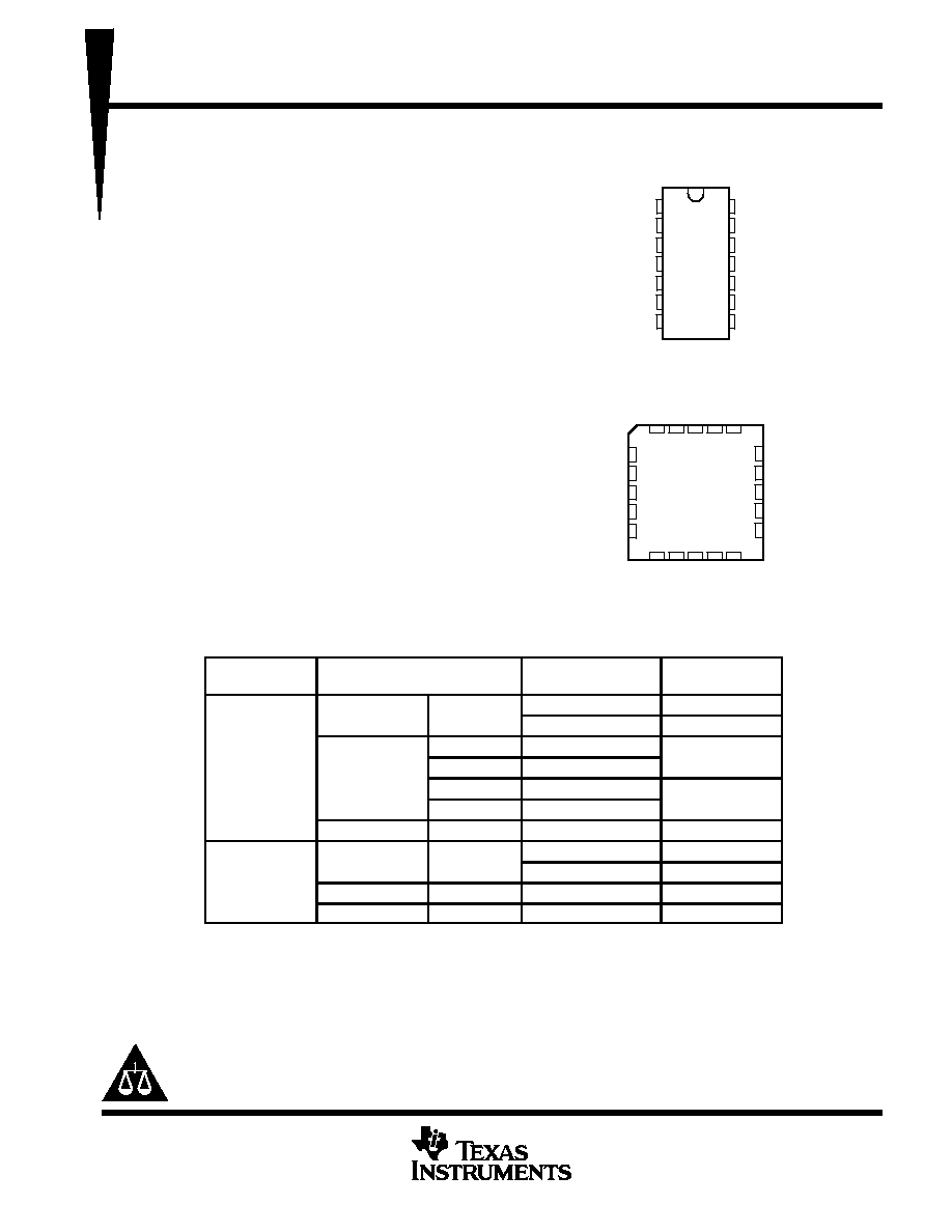
SN55110A . . . J OR W PACKAGE
SN75110A . . . D, N, OR NS PACKAGE
SN75112 . . . D OR N PACKAGE
(TOP VIEW)
3
2
1 20 19
9 10 11 12 13
4
5
6
7
8
18
17
16
15
14
1Z
NC
V
CC≠
NC
D
1C
NC
2C
NC
2A
SN55110A . . . FK PACKAGE
(TOP VIEW)
1B
1A
NC
2Z
1Y
2B
GND
NC
CC+
V
2Y
NC ≠ No internal connection
On products compliant to MIL-PRF-38535, all parameters are tested
unless otherwise noted. On all other products, production
processing does not necessarily include testing of all parameters.

SN55110A, SN75110A, SN75112
DUAL LINE DRIVERS
SLLS106F ≠ DECEMBER 1975 ≠ REVISED JULY 2003
2
POST OFFICE BOX 655303
∑
DALLAS, TEXAS 75265
description/ordering information (continued)
These drivers feature independent channels with common voltage supply and ground terminals. The significant
difference between the three drivers is in the output-current specification. The driver circuits feature a constant
output current that is switched to either of two output terminals by the appropriate logic levels at the input
terminals. The output current can be switched off (inhibited) by low logic levels on the enable inputs. The output
current is nominally 12 mA for the '110A devices, and is 27 mA for the SN75112.
The enable/inhibit feature is provided so the circuits can be used in party-line or data-bus applications. A strobe
or inhibitor (enable D), common to both drivers, is included for increased driver-logic versatility. The output
current in the inhibited mode, I
O(off)
, is specified so that minimum line loading is induced when the driver is used
in a party-line system with other drivers. The output impedance of the driver in the inhibited mode is very high.
The output impedance of a transistor is biased to cutoff.
The driver outputs have a common-mode voltage range of ≠3 V to 10 V, allowing common-mode voltage on the
line without affecting driver performance.
All inputs are diode clamped and are designed to satisfy TTL-system requirements. The inputs are tested at
2 V for high-logic-level input conditions and 0.8 V for low-logic-level input conditions. These tests ensure
400-mV noise margin when interfaced with TTL Series 54/74 devices.
The SN55110A is characterized for operation over the full military temperature range of ≠55
∞
C to 125
∞
C. The
SN75110A and SN75112 are characterized for operation from 0
∞
C to 70
∞
C.
FUNCTION TABLE
(each driver)
LOGIC
INPUTS
ENABLE
INPUTS
OUTPUTS
A
B
C
D
Y
Z
X
X
L
X
Off
Off
X
X
X
L
Off
Off
L
X
H
H
On
Off
X
L
H
H
On
Off
H
H
H
H
Off
On
H = high level, L = low level, X = irrelevant
When using only one channel of the line drivers,
the other channel should be inhibited and/or have
its outputs grounded.
SN55110A, SN75110A, SN75112
DUAL LINE DRIVERS
SLLS106F ≠ DECEMBER 1975 ≠ REVISED JULY 2003
3
POST OFFICE BOX 655303
∑
DALLAS, TEXAS 75265
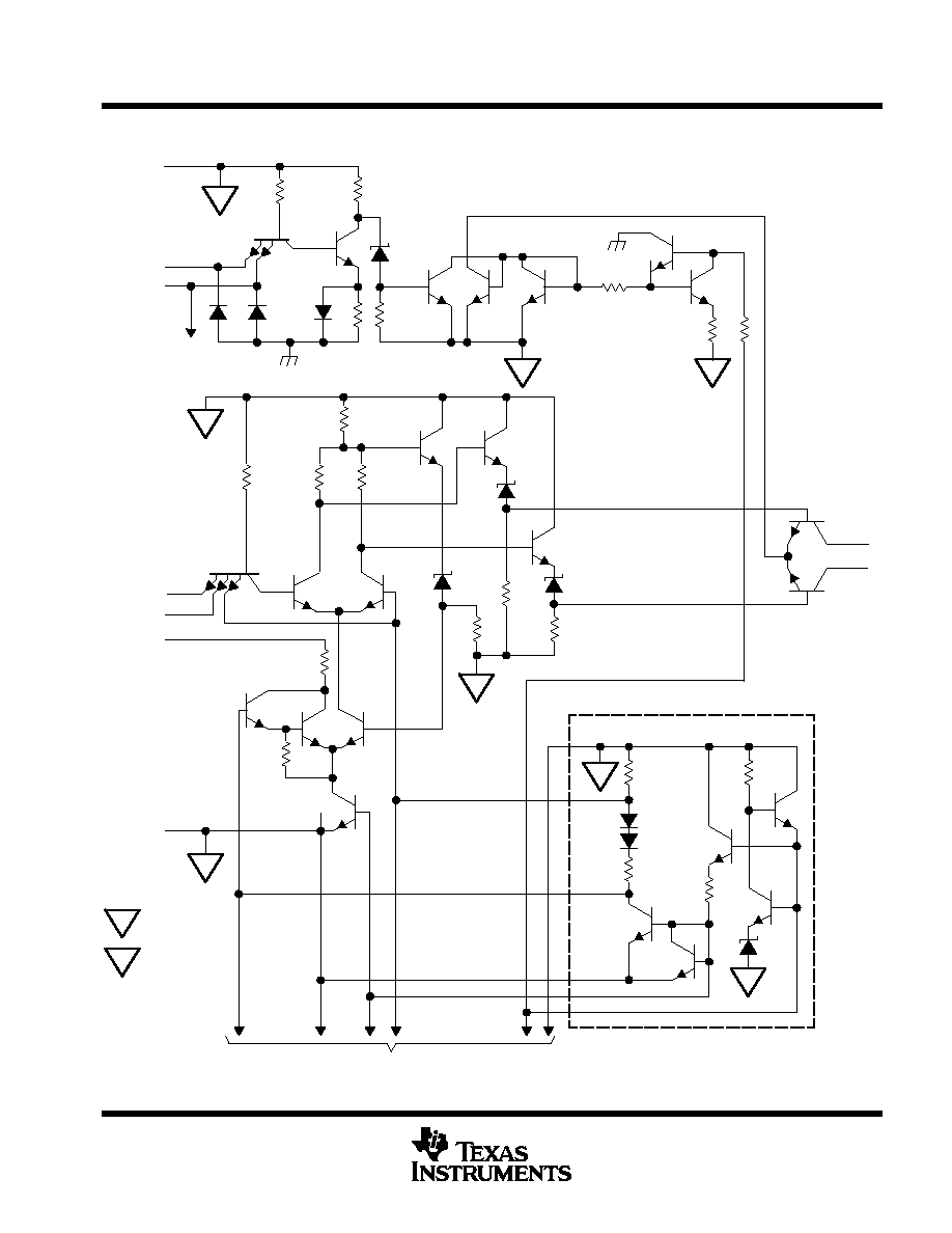
schematic (each driver)
To Other Driver
Y
Z
GND
B
A
. . . VCC+ Bus
. . . VCC≠ Bus
To Other
Driver
C
D
2.2 k
NOM
VCC≠
Common to Both Drivers
2.2 k
NOM
VCC+
Pin numbers shown are for the D, J, N, NS, and W packages.
+
≠
14
3, 4
10
1, 5
2, 6
7
11
8, 13
9, 12
+
≠
≠
≠
+
+
≠
≠
SN55110A, SN75110A, SN75112
DUAL LINE DRIVERS
SLLS106F ≠ DECEMBER 1975 ≠ REVISED JULY 2003
4
POST OFFICE BOX 655303
∑
DALLAS, TEXAS 75265
absolute maximum ratings over operating free-air temperature (unless otherwise noted)
Supply voltage: V
CC+
(see Note 1)
7 V
. . . . . . . . . . . . . . . . . . . . . . . . . . . . . . . . . . . . . . . . . . . . . . . . . . . . . . . . . . . .
V
CC≠
(see Note 1)
≠7 V
. . . . . . . . . . . . . . . . . . . . . . . . . . . . . . . . . . . . . . . . . . . . . . . . . . . . . . . . . .
Input voltage, V
I
5.5 V
. . . . . . . . . . . . . . . . . . . . . . . . . . . . . . . . . . . . . . . . . . . . . . . . . . . . . . . . . . . . . . . . . . . . . . . . . .
Output voltage range, V
O
≠5 V to 12 V
. . . . . . . . . . . . . . . . . . . . . . . . . . . . . . . . . . . . . . . . . . . . . . . . . . . . . . . . . . . .
Package thermal impedance,
JA
(see Notes 2 and 3): D package
86
∞
C/W
. . . . . . . . . . . . . . . . . . . . . . . . . . . .
N package
80
∞
C/W
. . . . . . . . . . . . . . . . . . . . . . . . . . . .
NS package
76
∞
C/W
. . . . . . . . . . . . . . . . . . . . . . . . . . .
Package thermal impedance,
JC
(see Notes 4 and 5): FK package
13.42
∞
C/W
. . . . . . . . . . . . . . . . . . . . . . . .
J package
15.05
∞
C/W
. . . . . . . . . . . . . . . . . . . . . . . . .
W package
14.65
∞
C/W
. . . . . . . . . . . . . . . . . . . . . . . .
Case temperature for 60 seconds: FK package
260
∞
C
. . . . . . . . . . . . . . . . . . . . . . . . . . . . . . . . . . . . . . . . . . . . . .
Lead temperature 1,6 mm (1/16 inch) from case for 60 seconds: J or W package
300
∞
C
. . . . . . . . . . . . . . . .
Lead temperature 1,6 mm (1/16 inch) from case for 10 seconds: D, N, or NS package
260
∞
C
. . . . . . . . . . . .
Storage temperature range, T
stg
≠65
∞
C to 150
∞
C
. . . . . . . . . . . . . . . . . . . . . . . . . . . . . . . . . . . . . . . . . . . . . . . . . .
Stresses beyond those listed under "absolute maximum ratings" may cause permanent damage to the device. These are stress ratings only, and
functional operation of the device at these or any other conditions beyond those indicated under "recommended operating conditions" is not
implied. Exposure to absolute-maximum-rated conditions for extended periods may affect device reliability.
NOTES:
1. Voltage values are with respect to network ground terminal.
2. Maximum power dissipation is a function of TJ(max),
JA, and TA. The maximum allowable power dissipation at any allowable
ambient temperature is PD = (TJ(max) ≠ TA)/
JA. Operating at the absolute maximum TJ of 150
∞
C can affect reliability.
3. The package thermal impedance is calculated in accordance with JESD 51-7.
4. Maximum power dissipation is a function of TJ(max),
JC, and TC. The maximum allowable power dissipation at any allowable case
temperature is PD = (TJ(max) ≠ TC)/
JC. Operating at the absolute maximum TJ of 150
∞
C can affect reliability.
5. The package thermal impedance is calculated in accordance with MIL-STD-883.
recommended operating conditions (see Note 6)
SN55110A
SN75110A
SN75112
UNIT
MIN
NOM
MAX
MIN
NOM
MAX
VCC+
Supply voltage
4.5
5
5.5
4.75
5
5.25
V
VCC≠
Supply voltage
≠4.5
≠5
≠5.5
≠4.75
≠5
≠5.25
V
Positive common-mode output voltage
0
10
0
10
V
Negative common-mode output voltage
0
≠3
0
≠3
V
VIH
High-level input voltage
2
2
V
VIL
Low-level output current
0.8
0.8
V
TA
Operating free-air temperature
≠55
125
0
70
∞
C
NOTE 6: When using only one channel of the line drivers, the other channel should be inhibited and/or have its outputs grounded.
SN55110A, SN75110A, SN75112
DUAL LINE DRIVERS
SLLS106F ≠ DECEMBER 1975 ≠ REVISED JULY 2003
5
POST OFFICE BOX 655303
∑
DALLAS, TEXAS 75265
electrical characteristics over recommended operating free-air temperature range (unless
otherwise noted)
PARAMETER
TEST CONDITIONS
SN55110A
SN75110A
SN75112
UNIT
MIN
TYP
MAX
MIN
TYP
MAX
VIK
Input clamp voltage
VCC
±
= MIN,
IL = ≠12 mA
≠0.9
≠1.5
≠0.9
≠1.5
V
VCC
±
= MAX,
VO = 10 V
12
15
27
40
IO( )
On state output current
VCC = MIN to MAX,
24
28
32
mA
IO(on)
On-state output current
CC
,
VO = ≠1 V to 1 V, TA = 25
∞
C
24
28
32
mA
VCC
±
= MIN,
VO = ≠3 V
6.5
12
15
27
IO(off)
Off-state output current
VCC
±
= MIN,
VO = 10 V
100
100
µ
A
II
Input current
at maximum
A, B, or C inputs
VCC
±
= MAX
VI = 5 5 V
1
1
mA
II
at maximum
input voltage
D input
VCC
±
= MAX,
VI = 5.5 V
2
2
mA
IIH
High-level
A, B, or C inputs
VCC
±
= MAX
VI = 2 4 V
40
40
µ
A
IIH
g
input current
D input
VCC
±
= MAX,
VI = 2.4 V
80
80
µ
A
IIL
Low-level
A, B, or C inputs
VCC
±
= MAX
VI = 0 4 V
≠3
≠3
mA
IIL
input current
D input
VCC
±
= MAX,
VI = 0.4 V
≠6
≠6
mA
ICC+(on)
Supply current from VCC
with driver enabled
VCC
±
= MAX,
A and B inputs at 0.4 V,
C and D inputs at 2 V
23
35
25
40
mA
ICC ( )
Supply current from VCC≠
VCC
±
= MAX,
A and B inputs at 0 4 V
34
50
65
100
mA
ICC≠(on)
y
CC
with driver enabled
A and B inputs at 0.4 V,
C and D inputs at 2 V
≠34
≠50
≠65
≠100
mA
ICC+(off)
Supply current from VCC≠
with driver inhibited
VCC
±
= MAX,
A, B, C, and D inputs at 0.4 V
21
30
mA
ICC≠(off)
Supply current from VCC
±
with driver inhibited
VCC
±
= MAX,
A, B, C, and D inputs at 0.4 V
≠17
≠32
mA
For conditions shown as MIN or MAX, use appropriate value specified under recommended operating conditions.
All typical values are at VCC+ = 5 V, VCC≠ = ≠5 V, TA = 25
∞
C.
switching characteristics, V
CC
±
=
±
5 V, T
A
= 25
∞
C (see Figure 1)
PARAMETERß
FROM
(INPUT)
TO
(OUTPUT)
TEST CONDITIONS
MIN
TYP
MAX
UNIT
tPLH
A or B
Y or Z
CL = 40 pF
RL = 50
9
15
ns
tPHL
A or B
Y or Z
CL = 40 pF,
RL = 50
,
9
15
ns
tPLH
C or D
Y or Z
CL = 40 pF
RL = 50
16
25
ns
tPHL
C or D
Y or Z
CL = 40 pF,
RL = 50
,
13
25
ns
ß tPLH = Propagation delay time, low- to high-level output
tPHL = Propagation delay time, high- to low-level output