
SN54HC377, SN74HC377
OCTAL D TYPE FLIP FLOPS
WITH CLOCK ENABLE
SCLS307B≠ JANUARY 1996 ≠ REVISED JANUARY 2003
1
POST OFFICE BOX 655303
∑
DALLAS, TEXAS 75265
D
Wide Operating Voltage Range of 2 V to 6 V
D
Outputs Can Drive Up To 10 LSTTL Loads
D
Low Power Consumption, 80-
µ
A Max I
CC
D
Typical t
pd
= 12 ns
D
±
4-mA Output Drive at 5 V
D
Low Input Current of 1
µ
A Max
D
Eight Flip-Flops With Single-Rail Outputs
D
Clock Enable Latched to Avoid False
Clocking
D
Applications Include:
≠ Buffer/Storage Registers
≠ Shift Registers
≠ Pattern Generators
description/ordering information
These devices are positive-edge-triggered octal
D-type flip-flops with an enable input. The 'HC377
devices are similar to the 'HC273 devices, but
feature a latched clock-enable (CLKEN) input
instead of a common clear.
Information at the data (D) inputs meeting the
setup time requirements is transferred to the
Q outputs on the positive-going edge of the clock
(CLK) pulse, if CLKEN is low. Clock triggering
occurs at a particular voltage level and is not
directly related to the transition time of the
positive-going pulse. When CLK is at either the
high or low level, the D input has no effect at the
output. These devices are designed to prevent
false clocking by transitions at CLKEN.
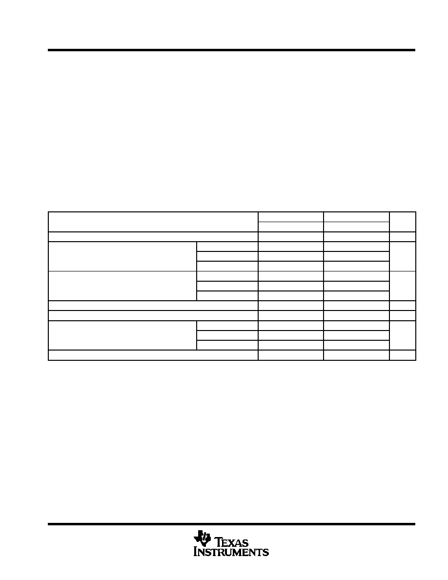
ORDERING INFORMATION
TA
PACKAGE
ORDERABLE
PART NUMBER
TOP-SIDE
MARKING
PDIP ≠ N
Tube
SN74HC377N
SN74HC377N
40
∞
C to 85
∞
C
SOIC
DW
Tube
SN74HC377DW
HC377
≠40
∞
C to 85
∞
C
SOIC ≠ DW
Tape and reel
SN74HC377DWR
HC377
SOP ≠ NS
Tape and reel
SN74HC377NSR
HC377
CDIP ≠ J
Tube
SNJ54HC377J
SNJ54HC377J
≠55
∞
C to 125
∞
C
CFP ≠ W
Tube
SNJ54HC377W
SNJ54HC377W
55 C to 125 C
LCCC ≠ FK
Tube
SNJ54HC377FK
SNJ54HC377FK
Package drawings, standard packing quantities, thermal data, symbolization, and PCB design guidelines are
available at www.ti.com/sc/package.
3
2 1 20 19
9 10 11 12 13
4
5
6
7
8
18
17
16
15
14
8D
7D
7Q
6Q
6D
2D
2Q
3Q
3D
4D
1D
1Q
CLKEN
5Q
5D
V
8Q
4Q
GND
CLK
SN54HC377 . . . FK PACKAGE
(TOP VIEW)
CC
SN54HC377 . . . J OR W PACKAGE
SN74HC377 . . . DW, N, OR NS PACKAGE
(TOP VIEW)
1
2
3
4
5
6
7
8
9
10
20
19
18
17
16
15
14
13
12
11
CLKEN
1Q
1D
2D
2Q
3Q
3D
4D
4Q
GND
V
CC
8Q
8D
7D
7Q
6Q
6D
5D
5Q
CLK
Copyright
2003, Texas Instruments Incorporated
Please be aware that an important notice concerning availability, standard warranty, and use in critical applications of
Texas Instruments semiconductor products and disclaimers thereto appears at the end of this data sheet.
PRODUCTION DATA information is current as of publication date.
Products conform to specifications per the terms of Texas Instruments
standard warranty. Production processing does not necessarily include
testing of all parameters.
On products compliant to MIL PRF 38535, all parameters are tested
unless otherwise noted. On all other products, production
processing does not necessarily include testing of all parameters.

SN54HC377, SN74HC377
OCTAL D TYPE FLIP FLOPS
WITH CLOCK ENABLE
SCLS307B≠ JANUARY 1996 ≠ REVISED JANUARY 2003
2
POST OFFICE BOX 655303
∑
DALLAS, TEXAS 75265
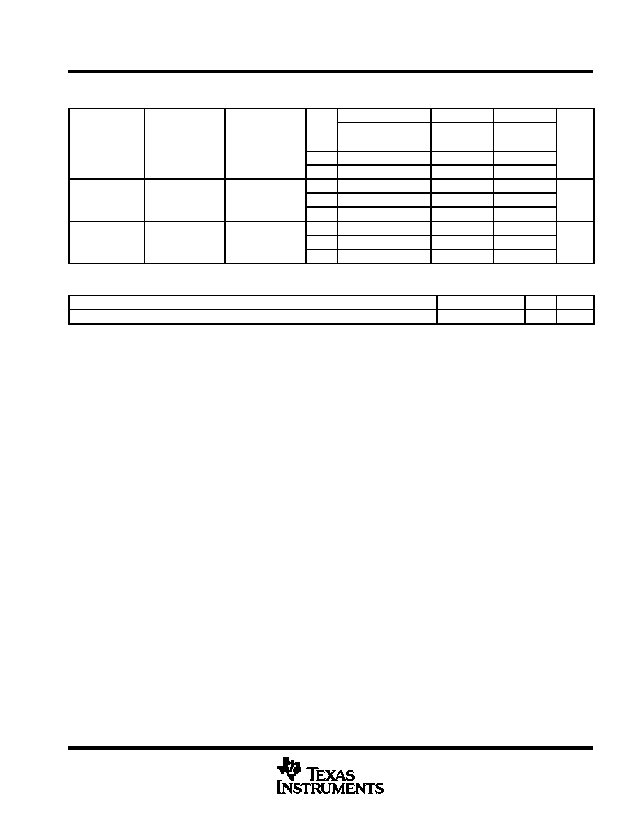
FUNCTION TABLE
(each flip-flop)
INPUTS
OUTPUT
CLKEN
CLK
D
OUTPUT
Q
H
X
X
Q0
L
H
H
L
L
L
X
L
X
Q0
logic diagram (positive logic)
CLKEN
1
11
3
2
CLK
1D
1Q
C1
1D
C1
1D
C1
1D
C1
1D
C1
1D
C1
1D
C1
1D
C1
1D
5
2Q
6
3Q
9
4Q
12
5Q
15
6Q
16
7Q
19
8Q
4
2D
7
3D
8
4D
13
5D
14
6D
17
7D
18
8D
SN54HC377, SN74HC377
OCTAL D TYPE FLIP FLOPS
WITH CLOCK ENABLE
SCLS307B≠ JANUARY 1996 ≠ REVISED JANUARY 2003
3
POST OFFICE BOX 655303
∑
DALLAS, TEXAS 75265
absolute maximum ratings over operating free-air temperature range (unless otherwise noted)
Supply voltage range, V
CC
≠0.5 V to 7 V
. . . . . . . . . . . . . . . . . . . . . . . . . . . . . . . . . . . . . . . . . . . . . . . . . . . . . . . . . .
Input clamp current, I
IK
(V
I
< 0 or V
I
> V
CC
) (see Note 1)
±
20 mA
. . . . . . . . . . . . . . . . . . . . . . . . . . . . . . . . . . . .
Output clamp current, I
OK
(V
O
< 0 or V
O
> V
CC
) (see Note 1)
±
20 mA
. . . . . . . . . . . . . . . . . . . . . . . . . . . . . . . .
Continuous output current, I
O
(V
O
= 0 to V
CC
)
±
25 mA
. . . . . . . . . . . . . . . . . . . . . . . . . . . . . . . . . . . . . . . . . . . . . .
Continuous current through V
CC
or GND
±
50 mA
. . . . . . . . . . . . . . . . . . . . . . . . . . . . . . . . . . . . . . . . . . . . . . . . . . .
Package thermal impedance,
JA
(see Note 2): DW package
58
∞
C/W
. . . . . . . . . . . . . . . . . . . . . . . . . . . . . . . . .
N package
69
∞
C/W
. . . . . . . . . . . . . . . . . . . . . . . . . . . . . . . . . . .
NS package
60
∞
C/W
. . . . . . . . . . . . . . . . . . . . . . . . . . . . . . . . .
Storage temperature range, T
stg
≠65
∞
C to 150
∞
C
. . . . . . . . . . . . . . . . . . . . . . . . . . . . . . . . . . . . . . . . . . . . . . . . . . .
Stresses beyond those listed under "absolute maximum ratings" may cause permanent damage to the device. These are stress ratings only, and
functional operation of the device at these or any other conditions beyond those indicated under "recommended operating conditions" is not
implied. Exposure to absolute-maximum-rated conditions for extended periods may affect device reliability.
NOTES:
1. The input and output voltage ratings may be exceeded if the input and output current ratings are observed.
2. The package thermal impedance is calculated in accordance with JESD 51-7.
recommended operating conditions (see Note 3)
SN54HC377
SN74HC377
UNIT
MIN
NOM
MAX
MIN
NOM
MAX
UNIT
VCC
Supply voltage
2
5
6
2
5
6
V
VCC = 2 V
1.5
1.5
VIH
High-level input voltage
VCC = 4.5 V
3.15
3.15
V
VIH
High level in ut voltage
VCC = 6 V
4.2
4.2
V
VCC = 2 V
0.5
0.5
VIL
Low-level input voltage
VCC = 4.5 V
1.35
1.35
V
VIL
Low level in ut voltage
VCC = 6 V
1.8
1.8
V
VI
Input voltage
0
VCC
0
VCC
V
VO
Output voltage
0
VCC
0
VCC
V
VCC = 2 V
1000
1000
t/
v
Input transition rise/fall time
VCC = 4.5 V
500
500
ns
t/
v
In ut transition rise/fall time
VCC = 6 V
400
400
ns
TA
Operating free-air temperature
≠55
125
≠40
85
∞
C
NOTE 3: All unused inputs of the device must be held at VCC or GND to ensure proper device operation. Refer to the TI application report,
Implications of Slow or Floating CMOS Inputs, literature number SCBA004.

SN54HC377, SN74HC377
OCTAL D TYPE FLIP FLOPS
WITH CLOCK ENABLE
SCLS307B≠ JANUARY 1996 ≠ REVISED JANUARY 2003
4
POST OFFICE BOX 655303
∑
DALLAS, TEXAS 75265
electrical characteristics over recommended operating free-air temperature range (unless
otherwise noted)
PARAMETER
TEST CONDITIONS
V
TA = 25
∞
C
SN54HC377
SN74HC377
UNIT
PARAMETER
TEST CONDITIONS
VCC
MIN
TYP
MAX
MIN
MAX
MIN
MAX
UNIT
2 V
1.9
1.998
1.9
1.9
IOH = ≠20
µ
A
4.5 V
4.4
4.499
4.4
4.4
VOH
VI = VIH or VIL
IOH 20
µ
A
6 V
5.9
5.999
5.9
5.9
V
VOH
VI VIH or VIL
IOH = ≠4 mA
4.5 V
3.98
4.3
3.7
3.84
V
IOH = ≠5.2 mA
6 V
5.48
5.8
5.2
5.34
2 V
0.002
0.1
0.1
0.1
IOL = 20
µ
A
4.5 V
0.001
0.1
0.1
0.1
VOL
VI = VIH or VIL
IOL 20
µ
A
6 V
0.001
0.1
0.1
0.1
V
VOL
VI VIH or VIL
IOL = 4 mA
4.5 V
0.17
0.26
0.4
0.33
V
IOL = 5.2 mA
6 V
0.15
0.26
0.4
0.33
II
VI = VCC or 0
6 V
±
0.1
±
100
±
1000
±
1000
nA
ICC
VI = VCC or 0,
IO = 0
6 V
8
160
80
µ
A
Ci
2 V to 6 V
3
10
10
10
pF
timing requirements over recommended operating free-air temperature range (unless otherwise
noted)
V
TA = 25
∞
C
SN54HC377
SN74HC377
UNIT
VCC
MIN
MAX
MIN
MAX
MIN
MAX
UNIT
2 V
5
3
4
fclock
Clock frequency
4.5 V
25
16
20
MHz
fclock
Clock frequency
6 V
29
19
23
MHz
2 V
100
150
125
tw
Pulse duration, CLK high or low
4.5 V
20
30
25
ns
tw
Pulse duration, CLK high or low
6 V
17
25
21
ns
2 V
100
150
125
D
4.5 V
20
30
25
t
Set p time before CLK
D
6 V
17
25
21
ns
tsu
Setup time before CLK
2 V
100
150
125
ns
CLKEN high or low
4.5 V
20
30
25
CLKEN high or low
6 V
17
25
21
2 V
5
5
5
th
Hold time after CLK
CLKEN inactive or active, data
4.5 V
5
5
5
ns
h
,
6 V
5
5
5
SN54HC377, SN74HC377
OCTAL D TYPE FLIP FLOPS
WITH CLOCK ENABLE
SCLS307B≠ JANUARY 1996 ≠ REVISED JANUARY 2003
5
POST OFFICE BOX 655303
∑
DALLAS, TEXAS 75265
switching characteristics over recommended operating free-air temperature range, C
L
= 50 pF
(unless otherwise noted) (see Figure 1)
PARAMETER
FROM
TO
V
TA = 25
∞
C
SN54HC377
SN74HC377
UNIT
PARAMETER
FROM
(INPUT)
TO
(OUTPUT)
VCC
MIN
TYP
MAX
MIN
MAX
MIN
MAX
UNIT
2 V
5
11
3
4
fmax
4.5 V
25
54
16
20
MHz
fmax
6 V
29
64
19
23
MHz
2 V
56
160
240
200
tpd
CLK
Any
4.5 V
15
32
48
40
ns
t d
CLK
Any
6 V
12
27
41
34
ns
2 V
38
75
110
95
tt
Any
4.5 V
8
15
22
19
ns
t
y
6 V
6
13
19
16
operating characteristics, T
A
= 25
∞
C
PARAMETER
TEST CONDITIONS
TYP
UNIT
Cpd
Power dissipation capacitance per flip-flop
No load
30
pF