
SN54ALS1035, SN74ALS1035
HEX NONINVERTING BUFFERS
WITH OPEN-COLLECTOR OUTPUTS
SDAS243B ≠ APRIL 1982 ≠ REVISED AUGUST 2001
1
POST OFFICE BOX 655303
∑
DALLAS, TEXAS 75265
D
Noninverting Buffers With
Open-Collector Outputs
description
These devices contain six independent
noninverting buffers. They perform the Boolean
function Y = A. The open-collector outputs require
pullup resistors to perform correctly. They can be
connected to other open-collector outputs to
implement active-low wired-OR or active-high
wired-AND functions. Open-collector devices are
often used to generate higher V
OH
levels.
ORDERING INFORMATION
TA
PACKAGE
ORDERABLE
PART NUMBER
TOP-SIDE
MARKING
SOIC
D
Tube
SN7ALS1035D
ALS1035
0
∞
C to 70
∞
C
SOIC ≠ D
Tape and reel
SN7ALS1035DR
ALS1035
PDIP ≠ N
Tube
SN74ALS1035N
SN74ALS1035N
CDIP ≠ J
Tube
SNJ54ALS1035J
SNJ54ALS1035J
≠55
∞
C to 125
∞
C
CFP ≠ W
Tube
SNJ54ALS1035W
SNJ54ALS1035W
LCCC - FK
Tube
SNJ54ALS1035FK
SNJ54ALS1035FK
Package drawings, standard packing quantities, thermal data, symbolization, and PCB design guidelines
are available at www.ti.com/sc/package.
FUNCTION TABLE
(each buffer)
INPUT
A
OUTPUT
Y
H
H
L
L
Copyright
2001, Texas Instruments Incorporated
Please be aware that an important notice concerning availability, standard warranty, and use in critical applications of
Texas Instruments semiconductor products and disclaimers thereto appears at the end of this data sheet.
SN54ALS1035 . . . FK PACKAGE
(TOP VIEW)
3
2
1 20 19
9 10 11 12 13
4
5
6
7
8
18
17
16
15
14
6Y
NC
5A
NC
5Y
2A
NC
2Y
NC
3A
1Y
1A
NC
4Y
4A
V
6A
3Y
NC
CC
NC ≠ No internal connection
GND
SN54ALS1035 . . . J OR W PACKAGE
SN74ALS1035 . . . D OR N PACKAGE
(TOP VIEW)
1
2
3
4
5
6
7
14
13
12
11
10
9
8
1A
1Y
2A
2Y
3A
3Y
GND
V
CC
6A
6Y
5A
5Y
4A
4Y
PRODUCTION DATA information is current as of publication date.
Products conform to specifications per the terms of Texas Instruments
standard warranty. Production processing does not necessarily include
testing of all parameters.
On products compliant to MIL-PRF-38535, all parameters are tested
unless otherwise noted. On all other products, production
processing does not necessarily include testing of all parameters.

SN54ALS1035, SN74ALS1035
HEX NONINVERTING BUFFERS
WITH OPEN-COLLECTOR OUTPUTS
SDAS243B ≠ APRIL 1982 ≠ REVISED AUGUST 2001
2
POST OFFICE BOX 655303
∑
DALLAS, TEXAS 75265
logic diagram (positive logic)
6A
6Y
5A
5Y
4A
4Y
3A
3Y
2A
2Y
1Y
1A
3
5
9
11
13
1
2
4
6
8
10
12
Pin numbers shown are for the D, J, N, and W packages.
absolute maximum ratings over operating free-air temperature range (unless otherwise noted)
Supply voltage, V
CC
7 V
. . . . . . . . . . . . . . . . . . . . . . . . . . . . . . . . . . . . . . . . . . . . . . . . . . . . . . . . . . . . . . . . . . . . . . . .
Input voltage, V
I
7 V
. . . . . . . . . . . . . . . . . . . . . . . . . . . . . . . . . . . . . . . . . . . . . . . . . . . . . . . . . . . . . . . . . . . . . . . . . . . .
Off-state output voltage
7 V
. . . . . . . . . . . . . . . . . . . . . . . . . . . . . . . . . . . . . . . . . . . . . . . . . . . . . . . . . . . . . . . . . . . . . .
Package thermal impedance,
JA
(see Note 1): D package
86
∞
C/W
. . . . . . . . . . . . . . . . . . . . . . . . . . . . . . . . . . .
N package
80
∞
C/W
. . . . . . . . . . . . . . . . . . . . . . . . . . . . . . . . . . .
Storage temperature range, T
stg
≠65
∞
C to 150
∞
C
. . . . . . . . . . . . . . . . . . . . . . . . . . . . . . . . . . . . . . . . . . . . . . . . . . .
Stresses beyond those listed under "absolute maximum ratings" may cause permanent damage to the device. These are stress ratings only, and
functional operation of the device at these or any other conditions beyond those indicated under "recommended operating conditions" is not
implied. Exposure to absolute-maximum-rated conditions for extended periods may affect device reliability.
1. The package thermal impedance is calculated in accordance with JESD 51-7.
recommended operating conditions
SN54ALS1035
SN74ALS1035
UNIT
MIN
NOM
MAX
MIN
NOM
MAX
UNIT
VCC
Supply voltage
4.5
5
5.5
4.5
5
5.5
V
VIH
High-level input voltage
2
2
V
VIL
Low-level input voltage
0.7
0.8
V
VOH
High-level output voltage
5.5
5.5
V
IOL
Low-level output current
12
24
mA
TA
Operating free-air temperature
≠ 55
125
0
70
∞
C

SN54ALS1035, SN74ALS1035
HEX NONINVERTING BUFFERS
WITH OPEN-COLLECTOR OUTPUTS
SDAS243B ≠ APRIL 1982 ≠ REVISED AUGUST 2001
3
POST OFFICE BOX 655303
∑
DALLAS, TEXAS 75265
electrical characteristics over recommended operating free-air temperature range (unless
otherwise noted)
PARAMETER
TEST CONDITIONS
SN54ALS1035
SN74ALS1035
UNIT
PARAMETER
TEST CONDITIONS
MIN
TYP
MAX
MIN
TYP
MAX
UNIT
VIK
VCC = 4.5 V,
II = ≠18 mA
≠1.5
≠1.5
V
VOL
VCC = 4 5 V
IOL = 12 mA
0.25
0.4
0.25
0.4
V
VOL
VCC = 4.5 V
IOL = 24 mA
0.35
0.5
V
IOH
VCC = 4.5 V,
VOH = 5.5 V
0.1
0.1
mA
II
VCC = 5.5 V,
VI = 7 V
0.1
0.1
mA
IIH
VCC = 5.5 V,
VI = 2.7 V
20
20
µ
A
IIL
VCC = 5.5 V,
VI = 0.4 V
≠ 0.1
≠ 0.1
mA
ICCH
VCC = 5.5 V,
VI = 4.5 V
3
6
3
6
mA
ICCL
VCC = 5.5 V,
VI = 0
8
14
8
14
mA
All typical values are at VCC = 5 V, TA = 25
∞
C.
switching characteristics (see Figure 1)
PARAMETER
FROM
(INPUT)
TO
(OUTPUT)
VCC = 4.5 V to 5.5 V,
CL = 50 pF,
RL = 680
,
TA = MIN to MAX
UNIT
(INPUT)
(OUTPUT)
SN54ALS1035
SN74ALS1035
MIN
MAX
MIN
MAX
tPLH
A
Y
5
35
5
30
ns
tPHL
A
Y
2
14
2
12
ns
For conditions shown as MIN or MAX, use the appropriate value specified under recommended operating conditions.
SN54ALS1035, SN74ALS1035
HEX NONINVERTING BUFFERS
WITH OPEN-COLLECTOR OUTPUTS
SDAS243B ≠ APRIL 1982 ≠ REVISED AUGUST 2001
4
POST OFFICE BOX 655303
∑
DALLAS, TEXAS 75265
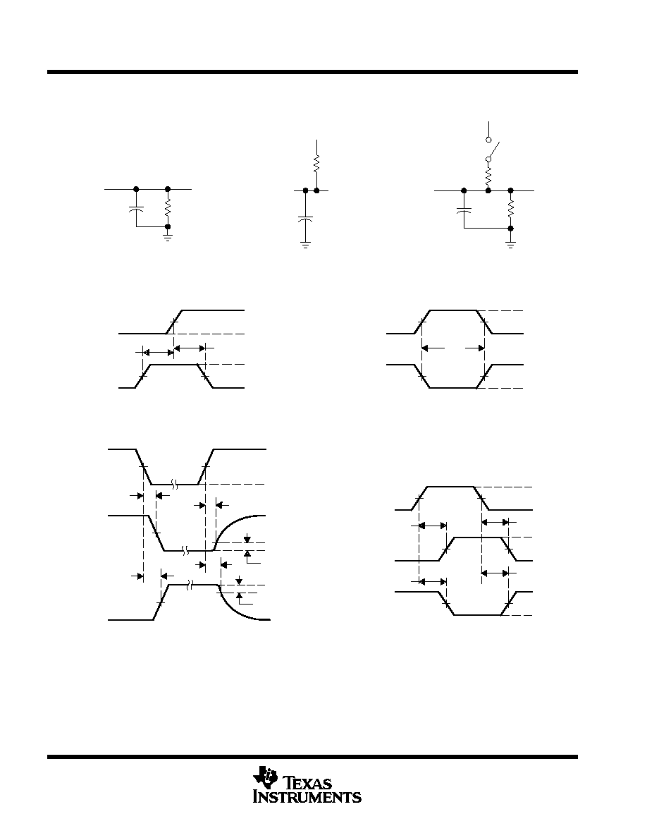
PARAMETER MEASUREMENT INFORMATION
SERIES 54ALS/ 74ALS AND 54AS/ 74AS DEVICES
tPHZ
tPLZ
tPHL
tPLH
0.3 V
tPZL
tPZH
tPLH
tPHL
LOAD CIRCUIT
FOR 3-STATE OUTPUTS
From Output
Under Test
Test
Point
R1
S1
CL
(see Note A)
7 V
1.3 V
1.3 V
1.3 V
3.5 V
3.5 V
0.3 V
0.3 V
th
tsu
VOLTAGE WAVEFORMS
SETUP AND HOLD TIMES
Timing
Input
Data
Input
1.3 V
1.3 V
3.5 V
3.5 V
0.3 V
0.3 V
High-Level
Pulse
Low-Level
Pulse
tw
VOLTAGE WAVEFORMS
PULSE DURATIONS
Input
Out-of-Phase
Output
(see Note C)
1.3 V
1.3 V
1.3 V
1.3 V
1.3 V
1.3 V
1.3 V
1.3 V
1.3 V
1.3 V
3.5 V
3.5 V
0.3 V
0.3 V
VOL
VOH
VOH
VOL
Output
Control
(low-level
enabling)
Waveform 1
S1 Closed
(see Note B)
Waveform 2
S1 Open
(see Note B)
[
0 V
VOH
VOL
[
3.5 V
In-Phase
Output
0.3 V
1.3 V
1.3 V
VOLTAGE WAVEFORMS
PROPAGATION DELAY TIMES
VOLTAGE WAVEFORMS
ENABLE AND DISABLE TIMES, 3-STATE OUTPUTS
R2
VCC
RL
Test
Point
From Output
Under Test
CL
(see Note A)
LOAD CIRCUIT
FOR OPEN-COLLECTOR OUTPUTS
LOAD CIRCUIT FOR
BI-STATE
TOTEM-POLE OUTPUTS
From Output
Under Test
Test
Point
CL
(see Note A)
RL
RL = R1 = R2
NOTES: A. CL includes probe and jig capacitance.
B. Waveform 1 is for an output with internal conditions such that the output is low except when disabled by the output control.
Waveform 2 is for an output with internal conditions such that the output is high except when disabled by the output control.
C. When measuring propagation delay items of 3-state outputs, switch S1 is open.
D. All input pulses have the following characteristics: PRR
1 MHz, tr = tf = 2 ns, duty cycle = 50%.
E. The outputs are measured one at a time with one transition per measurement.
Figure 1. Load Circuits and Voltage Waveforms

IMPORTANT NOTICE
Texas Instruments and its subsidiaries (TI) reserve the right to make changes to their products or to discontinue
any product or service without notice, and advise customers to obtain the latest version of relevant information
to verify, before placing orders, that information being relied on is current and complete. All products are sold
subject to the terms and conditions of sale supplied at the time of order acknowledgment, including those
pertaining to warranty, patent infringement, and limitation of liability.
TI warrants performance of its products to the specifications applicable at the time of sale in accordance with
TI's standard warranty. Testing and other quality control techniques are utilized to the extent TI deems necessary
to support this warranty. Specific testing of all parameters of each device is not necessarily performed, except
those mandated by government requirements.
Customers are responsible for their applications using TI components.
In order to minimize risks associated with the customer's applications, adequate design and operating
safeguards must be provided by the customer to minimize inherent or procedural hazards.
TI assumes no liability for applications assistance or customer product design. TI does not warrant or represent
that any license, either express or implied, is granted under any patent right, copyright, mask work right, or other
intellectual property right of TI covering or relating to any combination, machine, or process in which such
products or services might be or are used. TI's publication of information regarding any third party's products
or services does not constitute TI's approval, license, warranty or endorsement thereof.
Reproduction of information in TI data books or data sheets is permissible only if reproduction is without
alteration and is accompanied by all associated warranties, conditions, limitations and notices. Representation
or reproduction of this information with alteration voids all warranties provided for an associated TI product or
service, is an unfair and deceptive business practice, and TI is not responsible nor liable for any such use.
Resale of TI's products or services with
statements different from or beyond the parameters stated by TI for
that product or service voids all express and any implied warranties for the associated TI product or service,
is an unfair and deceptive business practice, and TI is not responsible nor liable for any such use.
Also see: Standard Terms and Conditions of Sale for Semiconductor Products. www.ti.com/sc/docs/stdterms.htm
Mailing Address:
Texas Instruments
Post Office Box 655303
Dallas, Texas 75265
Copyright
2001, Texas Instruments Incorporated